Selecting SMD electronic components requires more than matching a value and package name. The chosen part must satisfy the circuit, fit the verified PCB footprint, survive the operating environment, remain available for production, and be compatible with placement, soldering, inspection and testing. A smaller or cheaper component is not a better choice if it reduces electrical margin, creates an uninspectable joint or introduces supply risk.
SMD means surface-mount device; SMT is the process used to assemble that device onto a PCB. Electrical and footprint decisions should be reviewed together with the manufacturer part number, lifecycle, traceability and approved alternatives. The most reliable result comes when the component and assembly process are evaluated as one system.
Which Requirements Should You Define Before Selecting SMD Electronic Components?
Begin with measurable product requirements, not a distributor filter. Define the circuit function, normal and worst-case loads, operating environment, board constraints, production volume and service life before comparing parts. Otherwise, an apparently suitable component may fail when temperature, transient energy or mechanical stress is considered.
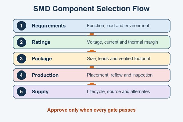
- Electrical conditions: Record nominal, minimum and maximum voltage, current, power, frequency, tolerance and transient conditions.
- Mechanical limits: Define available board area, component height, connector forces, shock, vibration and enclosure constraints.
- Environmental limits: Specify operating temperature, humidity, contamination exposure and any required product grade.
- Production conditions: State prototype and forecast quantities, assembly sides, expected rework and inspection requirements.
- Commercial limits: Establish target cost, approved manufacturers, lifecycle expectations and acceptable lead-time risk.
How Do You Choose Between SMD, Through-Hole and Mixed PCB Assembly?
Match the assembly method to the product. Choose SMD for density and automated production, through-hole for selected mechanical or high-power needs, and mixed assembly when both are required. Make this decision before package selection because it affects layout, tooling, soldering and cost. Products with stressed connectors, large magnetic parts or frequent manual servicing may also benefit from selected through-hole mounting practices rather than an all-SMD layout.
| Assembly choice | Best fit | Main trade-off |
| SMD | Compact products, short interconnects and automated volume assembly | Very small or hidden-joint packages may increase process and inspection demands |
| Through-hole | Large transformers, some high-power parts and mechanically stressed connections | Uses more board area and may require additional assembly operations |
| Mixed | Products combining dense electronics with large, heavy or stressed components | Requires careful process sequencing and may increase handling and tooling |
How Do You Choose Among the Main Types of SMD Electronic Components?
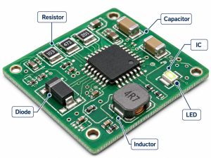
Select the component technology from the required circuit behavior, then compare packages. A capacitance or resistance value alone does not describe bias behavior, pulse capability, noise, losses or stability.
| Circuit task | Common SMD component | Selection focus |
| Biasing or current limiting | Thick-film or thin-film resistor | Tolerance, temperature coefficient, working voltage and pulse load |
| Decoupling or filtering | MLCC, film or electrolytic capacitor | Effective capacitance, voltage bias, ESR, ripple and polarity |
| Energy storage in switching power | Power inductor | Inductance under DC bias, saturation current, temperature-rise current, DCR and core loss |
| RF matching or filtering | RF inductor | Q factor, self-resonant frequency, impedance at the operating frequency and tolerance |
| Common-mode noise suppression | Common-mode choke | Common-mode impedance, differential-mode impact, rated current and insulation |
| Rectification or protection | Rectifier, Schottky, TVS or Zener diode | Reverse voltage, forward current, surge energy and leakage |
| Power switching | MOSFET or bipolar transistor | Voltage, current, safe operating area, conduction loss, switching loss and thermal path |
| Control, logic or signal processing | Integrated circuit | Supply range, I/O levels, required function, timing, pinout and package |
Keep category boundaries clear. A ferrite bead, for example, may resemble a chip inductor but is normally selected by impedance-versus-frequency behavior and current rating rather than by inductance alone.
How Do You Determine the Required Electrical Ratings and Safety Margins?
Use worst-case conditions and documented derating. Electrical ratings for SMD electronic components must account for voltage, current, power, tolerance, temperature coefficient, frequency behavior, surge or pulse loading and expected aging. The correct margin depends on the component technology, duty cycle, ambient temperature, PCB cooling and reliability target.
For resistors, confirm both power and maximum working voltage. For MLCCs, evaluate effective capacitance after DC bias, tolerance and temperature effects. For inductors, distinguish saturation current from temperature-rise current. For semiconductors, calculate junction temperature from actual losses and the complete thermal path. Manufacturer datasheets and application notes should control these decisions; a universal derating percentage is rarely defensible across all SMD electronic components.
Worked example: Assume a resistor must drop 12 V at 10 mA. The required resistance is 12 V / 0.01 A = 1.2 kΩ, and the calculated dissipation is 12 V × 0.01 A = 0.12 W. If this project limits continuous dissipation to 50% of the rated power, the minimum rating is 0.24 W. A 0.25 W part only just clears that project gate, so its maximum working voltage and temperature derating still need to be checked; the next power rating may be the safer choice. The 50% limit is an example project rule, not a universal requirement.
How Do You Compare SMD Component Packages and Sizes?
Eliminate every package that fails a mandatory requirement. Then choose the smallest option that passes all five steps. This SMD component size selection method prevents board-area savings from overriding electrical or production limits.
- Check the electrical rating. Reject sizes that cannot handle the worst-case voltage, current, power or pulse load.
- Check technology-specific behavior. Verify resistor working voltage, MLCC capacitance under DC bias, or semiconductor losses as applicable.
- Check the thermal path. Reject power packages that cannot transfer the calculated heat through the available copper and airflow.
- Check physical and assembly limits. Confirm height, terminal geometry, pad area, placement, inspection and rework access.
- Choose between the passing sizes. Compare at least two exact part datasheets and select the smaller option only when it adds no unnecessary production risk.
Chip-passive codes such as 0402, 0603 and 0805 may use imperial notation, while metric codes describe different physical dimensions. Confirm the actual length and width in the datasheet rather than relying on the code alone. For SOT, SOIC, TSSOP, QFP, QFN, DFN and BGA families, compare body dimensions, terminal pitch, standoff, exposed-pad geometry and package height—not only the family name.
How Do You Choose the Right Lead, Termination and Package Configuration?
Balance density, heat transfer and joint visibility. The correct configuration must also fit the available assembly and inspection process. Apply these package-specific checks:
- Chip terminations: Use them for most resistors, capacitors and other passives; verify the exact body size and end-metallization dimensions.
- Gull-wing leads: Prefer SOIC, TSSOP or QFP when visible joints, probing and rework access matter, while allowing enough perimeter area.
- J-leads: Use them when perimeter space must be reduced, but account for lower joint visibility and more difficult inspection.
- QFN and DFN: Choose them for compact size, short electrical paths or exposed-pad heat transfer only when paste control and X-ray inspection are available.
- BGA and CSP: Use area-array packages when interconnect density or routing demands them; confirm escape routing, X-ray capability and a practical rework strategy.
- Final release checks: Verify the exact pinout, polarity or pin 1, exposed-pad function, pitch, terminal width, package height, thermal-pad geometry and manufacturer part-number suffix.
How Do You Verify That the SMD Package Matches the PCB Footprint?
Verify the exact orderable part number. For SMD electronic components, a matching package-family name does not prove that the PCB footprint is compatible. Use the latest controlled datasheet and an applicable land-pattern method such as IPC-7351, then complete these checks:
- Package dimensions: Match terminal count, pitch, body size, terminal geometry, standoff and maximum component height.
- Land pattern: Start from the manufacturer’s recommendation and adjust it only for a documented soldering or reliability need.
- Pin mapping: Confirm pin numbering, electrical pinout, polarity and pin-1 orientation against the schematic symbol.
- Thermal features: Check exposed-pad dimensions, paste segmentation, thermal vias and possible solder wicking.
- Assembly clearance: Verify courtyard, nozzle access, neighboring-part height, inspection visibility and rework space.
- Library release: Link the approved symbol, footprint, 3D body and manufacturer part number, then run a documented peer check.
How Do You Evaluate Thermal and Environmental Suitability?
Keep every worst-case exposure within documented limits. Thermal approval of SMD electronic components must include the required operating margin, not only the headline temperature rating. Review the following conditions separately:
- Power loss: Calculate dissipation at maximum load, including duty cycle, switching loss, surge events and tolerance extremes where relevant.
- Heat path: Include ambient temperature, nearby heat sources, PCB copper, thermal vias, airflow and the enclosure instead of relying on a package rating alone.
- Thermal data: Use thermal-resistance values only when the datasheet test board and boundary conditions reasonably represent the intended layout.
- Environmental exposure: Check humidity, vibration, mechanical shock, corrosive gases and temperature cycling against the product specification.
- Required grade: Request the exact qualification and supporting documentation; temperature range alone does not establish automotive or industrial suitability.
- Moisture sensitivity: Confirm MSL, floor life, dry storage and baking instructions from the component label and applicable J-STD-020/J-STD-033 controls.
How Do Placement, Soldering and Reflow Requirements Affect Component Selection?
Reject parts that fall outside the available process. Packaging, pickup surface, terminal geometry and temperature limits for SMD electronic components must suit the placement and soldering equipment. Confirm tape, tray or tube format, feeder compatibility, component dimensions, pickup area, centroid accuracy and rotation before release. Small passives, fine-pitch leads, bottom-terminated packages and high-thermal-mass parts each require a different process window.
Review stencil aperture design, paste type, PCB finish, component termination and reflow limitations together. Avoid assigning one universal reflow temperature to an entire BOM: the approved profile depends on solder paste, board construction, component temperature limits and thermal distribution across the assembly. Mixed package sizes can make it difficult to achieve sufficient wetting without overheating sensitive parts.
How Should Inspection and Testability Influence SMD Component Selection?
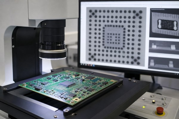
Select packages whose critical defects can be detected. Inspection plans for SMD electronic components should match joint visibility and the applicable acceptance criteria. AOI is effective for visible leads, polarity, presence and many solder-joint conditions, but it cannot directly view joints under QFN, LGA or BGA bodies. X-ray can reveal hidden-joint alignment, opens, bridges and void patterns. This limitation is also reflected in Analog Devices’ QFN assembly guidance, which describes transmission X-ray for post-reflow evaluation of concealed joints.
| Package characteristic | Verification stage and method | Remaining blind spot |
| Visible chip or gull-wing joints | Before placement: SPI checks solder-paste deposits. After reflow: AOI or first-article inspection checks presence, polarity and visible joints. | Internal component damage or marginal electrical performance |
| Bottom-terminated QFN or LGA | Before placement: SPI checks paste deposits. After reflow: X-ray evaluates concealed joints; electrical or functional test is added where applicable. | Some interface defects may require process correlation or destructive analysis |
| BGA or CSP | Before placement: SPI checks paste deposits. After reflow: X-ray evaluates the ball array; functional or boundary-scan test is added where supported. | Intermittent defects may not appear in a static image |
Design test points and programming access before layout is frozen. If a package eliminates probe access, the test strategy must compensate through connectors, boundary scan, built-in diagnostics or functional fixtures. A documented electronic product development testing plan should connect these access decisions to prototype, first-article and production acceptance tests.
How Do You Assess Component Availability, Lifecycle and Sourcing Risks?
Approve alternatives before a shortage occurs. Supply-risk reviews for SMD electronic components must use the exact part number; distributor stock alone does not make a part production-ready. Complete these checks:
- Lifecycle status: Check active, NRND and end-of-life status, together with product-change and discontinuance notices.
- Source coverage: Confirm availability through authorized channels and avoid dependence on one unverified source.
- Order constraints: Review lead time, minimum order quantity, price breaks, packaging format and stock distribution for the planned build volume.
- Traceability: Require the exact manufacturer part number, manufacturer identity, lot or date information and original packaging records as applicable.
- Alternate validation: Compare electrical behavior, ratings, dimensions, pinout, materials, MSL, reflow limits and required regulatory documentation.
- Change control: Record approved alternates in the BOM and require documented review before any substitution reaches production.
- Long-life planning: Monitor lead-time movement and manufacturer changes early enough to qualify a replacement or revise the design without stopping a build.
Which SMD Component Selection Mistakes Cause PCB Assembly Defects?
Many apparent soldering defects begin with a component, footprint or documentation decision. The defect still requires process evidence before assigning a root cause, but selection reviews can remove common contributors early.
| Observed defect | Possible component, footprint or process contributors | Verification |
| Tombstoning or skew | Unbalanced pads, unequal termination wetting or unsuitable passive geometry | Check land pattern, paste deposits, placement and thermal balance |
| Bridging | Fine pitch, excessive paste or mismatched terminal geometry | Compare footprint, stencil data, SPI and reflow evidence |
| Insufficient solder or opens | Incorrect pad dimensions, poor coplanarity or paste-release limitations | Inspect paste transfer, package dimensions and joint formation |
| Voiding under thermal pad | Large exposed pad without suitable paste and via strategy | Review stencil segmentation, via design, profile and X-ray result |
| Cracked MLCC | Package placement in a high-flex board area or mechanical handling stress | Review layout location, depaneling, fasteners and failure analysis |
| Wrong or reversed part | Ambiguous BOM, markings, polarity or centroid rotation | Reconcile material-release records, kitting, assembly drawing and first article |
How Do You Compare Candidate SMD Components and Make the Final Decision?
Reject any candidate that fails a mandatory requirement. Compare candidate SMD electronic components in a decision matrix, but do not let a low unit price compensate for an incompatible footprint, inadequate rating or unavailable inspection method. Score optional advantages only after all gates pass.
| Decision gate | Required evidence | Owner |
| Circuit performance | Worst-case calculations, simulation or test plan and datasheet limits | Design review |
| Package and footprint | Controlled datasheet-to-library comparison | PCB design |
| Thermal and environmental fit | Thermal analysis and application requirements | Technical and quality review |
| Assembly and inspection | DFM review, process capability and inspection plan | Production review |
| Supply continuity | Lifecycle, authorized-source availability and approved alternates | Supply review |
| Final approval | Exact MPN, revision-controlled BOM and validation status | Cross-functional approval |
For a new design, validate high-risk packages and substitutions through prototypes or a first-article build. Record the evidence behind the approved choice so later cost reductions or shortage substitutions do not erase the original technical constraints.
What Should Be Included in the Final BOM and PCB Assembly Package?
Release only exact, verifiable part data. The final package for SMD electronic components must state the approved part, placement information and finished-assembly verification requirements. Ambiguity transfers avoidable decisions into material preparation or production.
- BOM: Include reference designators, quantity, description, exact manufacturer, MPN, package, lifecycle information and approved alternates.
- PCB data: Supply Gerber or ODB++, fabrication information and the controlled board revision.
- Placement data: Provide centroid coordinates, side, rotation and consistent design origins.
- Assembly drawing: Show polarity, pin 1, special mounting, do-not-fit parts and process notes.
- Process controls: Identify moisture-sensitive handling, baking, special soldering and cleanliness requirements.
- Test requirements: Define inspection, programming, in-circuit or functional testing and acceptance criteria.
FAQs About Selecting SMD Electronic Components
Q1: How can you identify an unmarked SMD component on an assembled board?
A1: Match its reference designator to the controlled BOM and placement data, then verify the original reel or tray label when available. Appearance alone is not reliable enough to establish an exact orderable part number.
Q2: Can a zero-ohm SMD resistor be selected only by package size?
A2: No. Also check its current rating, maximum resistance, pulse capability and jumper function. A zero-ohm marking does not mean zero loss or unlimited current.
Q3: Can a ferrite bead replace an SMD inductor?
A3: Not as a direct substitute. A ferrite bead is normally specified by impedance over frequency and DC current, while an inductor is selected by inductance, bias behavior, saturation and loss.
Q4: Are all SMD capacitors polarized?
A4: No. Standard ceramic MLCCs are generally nonpolar, while aluminum electrolytic, tantalum and some specialty capacitors require correct orientation. Follow the exact datasheet and polarity marking rather than assuming from package shape.
Q5: When should a soft-termination MLCC be considered?
A5: Consider it where board flex, depaneling, vibration or thermal cycling creates a credible cracking risk. The termination option reduces mechanical stress but does not replace good component placement and board handling.
Q6: When is an anti-sulfur SMD resistor useful?
A6: It is useful where sulfur-bearing gases or materials may attack conventional silver-based terminations, such as some industrial, automotive or polluted environments. Confirm the required test condition and component qualification.
Q7: Must an IC exposed pad always be soldered to the PCB?
A7: Follow the exact datasheet. An exposed pad may provide heat transfer, electrical connection or both; leaving it unsoldered can cause overheating or functional failure when attachment is required.
Q8: Can a component top marking be used as the orderable part number?
A8: Usually not. Top marks may be abbreviated, shared across variants or combined with lot codes. Use the controlled BOM and packaging traceability to identify the exact part.
Q9: What should happen if a reel label differs from the BOM description?
A9: Stop material release and reconcile the exact manufacturer part number, package, value, lot and approved-alternate status. Do not place the part based only on a similar description.
Q10: Why can an MLCC make an audible buzzing or whining sound?
A10: Some ceramic dielectrics exhibit piezoelectric behavior, so changing voltage can make the capacitor and PCB vibrate. Capacitor construction, placement, board stiffness and the excitation waveform can all affect the noise.
Conclusion
A reliable component list is one that can be placed, soldered, inspected, tested and sourced without forcing last-minute changes. Finalize each selection at the exact manufacturer-part-number level and keep footprints, approved alternatives and assembly requirements under revision control.
Check package and production compatibility before release. Let EBest Circuit review whether your selected SMD electronic components, footprints and production requirements work together. Email your Gerber or ODB++ data, BOM with manufacturer part numbers and approved alternatives, build quantity, stackup, assembly drawings, programming method and test requirements to sales@bestpcbs.com. We will review package-to-footprint fit, assembly risks and inspection needs, then return practical feedback with a quotation for manufacturing quotation support.