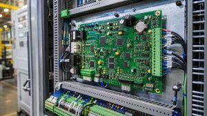
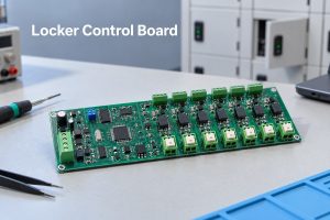
A security monitoring PCB must detect alarm signals accurately, maintain stable communication, and operate reliably around the clock. Unstable sensor inputs, electrical interference, poor solder connections, and power disturbances can cause false alarms, missed events, or equipment shutdowns. How can these risks be reduced without adding unnecessary manufacturing complexity or cost?
EBest Circuit provides factory-direct security monitoring PCB manufacturing and assembly services, including custom multilayer PCB fabrication, SMT/THT assembly, component sourcing, and functional testing. We support intrusion detection controllers, alarm monitoring boards, perimeter security equipment, and communication interface PCBs from prototyping to mass production, with a free DFM check before manufacturing.
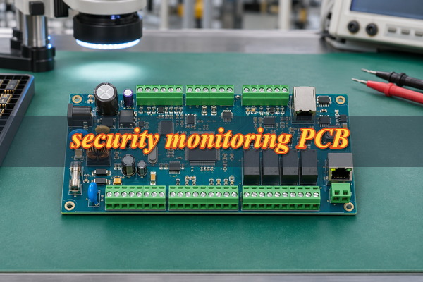
What Causes Signal Failures and False Alarms in Security Monitoring PCBs?
Security monitoring PCB signal failures commonly result from unstable input circuits, power disturbances, defective connections, and electrical interference. However, a false alarm may also originate from the sensor, external wiring, or firmware rather than the PCB itself.
The most common PCB-related causes include:
- Unstable sensor inputs: Electrical noise, incorrect input resistance, or excessive leakage current may cause the controller to detect an unintended alarm state.
- Power supply disturbances: Relay switching, insufficient decoupling, or excessive voltage drop can reset the controller or interrupt signal processing.
- Electromagnetic interference: Switching power supplies, motors, and long field cables may introduce unwanted signals into sensitive monitoring circuits.
- Soldering and connector defects: Cracked solder joints, insufficient solder, and poor terminal connections can produce intermittent failures.
- Communication faults: Incorrect termination, damaged traces, or unreliable connections may interrupt Ethernet or RS-485 communication.
- Moisture and contamination: Condensation, ionic residues, and corrosion can increase leakage currents or damage electrical connections.
For example, an alarm controller that resets when a relay operates may have inadequate power decoupling or insufficient transient suppression. If only one sensor channel produces intermittent alarms, the input circuit, terminal connection, and field wiring should be investigated first.
Fault diagnosis should begin with measured input signals, supply voltages, and communication status. These measurements help distinguish PCB defects from sensor, wiring, and software problems before unnecessary design changes are made.
What Are the Key Design Parameters for Security Monitoring PCB Reliability?
Security monitoring PCB reliability depends on the layer structure, copper thickness, electrical clearances, material selection, and manufacturing tolerances. These parameters must support the required sensor channels, communication interfaces, power distribution, and mechanical installation.
The following table combines common design references with EBest Circuit’s relevant FR-4 PCB manufacturing capabilities.
| PCB Parameter | Design Reference / Manufacturing Capability | Engineering Consideration |
|---|---|---|
| PCB Layers | 2–4 layers common; EBest standard 1–10 layers, special up to 32 | Routing density, grounding, and signal integrity |
| PCB Material | Standard or high-Tg FR-4 | Thermal requirements and assembly conditions |
| Board Thickness | 1.0–1.6 mm common; EBest standard 0.4–3.5 mm | Enclosure fit, connectors, and mechanical loading |
| Copper Weight | EBest standard: 0.5–5 oz inner, 1–5 oz outer | Current capacity, temperature rise, and trace geometry |
| Minimum Trace / Space | 4/4 mil standard at applicable copper weights; 3/3 mil special | Copper thickness and fabrication feasibility |
| Finished Mechanical Hole | 0.20 mm standard; 0.15 mm special | Hole plating and aspect ratio |
| Ethernet Differential Impedance | Typically 100 Ω | PHY specifications and controlled-impedance stackup |
| RS-485 Termination | Commonly 120 Ω at each physical bus end | Cable characteristic impedance and network topology |
| Creepage / Clearance | Based on working voltage and applicable safety requirements | Isolation, surge protection, and installation environment |
| Surface Finish | ENIG, lead-free HASL, OSP | Component pitch, solderability, and assembly requirements |
Manufacturing limits cannot automatically be combined in one PCB design. Fine-line processing, heavy copper, small finished holes, and high layer counts must be evaluated against the complete stackup.
For a security monitoring controller combining Ethernet, relay outputs, multiple sensor channels, and switching power supplies, a four-layer PCB may provide better routing flexibility and reference-plane continuity than a crowded two-layer structure.
Connector mounting also deserves attention. Field wiring terminals may experience repeated mechanical loading during installation and maintenance, making PCB thickness, mounting support, and solder-joint reliability important considerations.
Final manufacturing feasibility should be confirmed using the approved PCB stackup, copper distribution, drill files, mechanical drawing, and assembly requirements.
How Can Security Monitoring PCBs Maintain Stable Sensor and Alarm Signal Transmission?
Stable signal transmission requires correct input conditioning, controlled PCB routing, reliable connectors, and appropriate communication termination. Different alarm and monitoring interfaces need different electrical requirements.
The main design considerations include:
- Digital alarm inputs: Use defined logic thresholds, suitable pull-up or pull-down networks, and debounce filtering to prevent unintended switching.
- Supervised alarm loops: Apply the specified end-of-line resistor arrangement to distinguish normal, alarm, open-circuit, and short-circuit conditions.
- Analog sensor inputs: Keep sensitive traces separated from switching regulators, relay drivers, and high-current return paths.
- RS-485 communication: Use appropriate termination, minimize branch stubs, and verify grounding and common-mode voltage requirements.
- Ethernet communication: Maintain the required differential impedance and follow the PHY manufacturer’s routing recommendations.
- Field connectors: Verify terminal assignments, solder-joint integrity, mechanical support, and contact reliability.
For example, a supervised intrusion detector may report different resistance states for normal operation, an alarm, and a wiring fault. Incorrect resistor values, excessive leakage, or an intermittent PCB terminal connection can cause the controller to interpret the wrong state.
Filtering must also match the required response time. Excessive filtering may delay valid alarm events, while insufficient filtering can allow short electrical disturbances to trigger unwanted alarms.
EBest Circuit manufactures security monitoring PCBs according to the approved circuit and layout specifications, with attention to trace geometry, component footprints, connector assembly, and soldering quality. Alarm thresholds and response timing must be verified through customer-defined functional testing.
How Can Security Monitoring PCBs Withstand EMI, ESD, and Power Surges?
Security monitoring PCBs require suitable electrical protection at external power, sensor, and communication interfaces. Long field cables and exposed connectors can carry electrical disturbances into the board, potentially causing signal errors, damaged components, or controller resets.
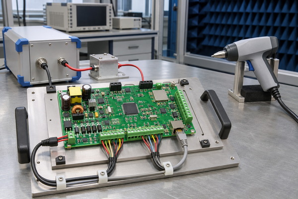
The following protection measures address different electrical risks:
- ESD protection: Place appropriately rated TVS devices close to exposed connectors and use short return paths.
- Surge protection: Select protective components according to the specified transient waveform, voltage, and installation conditions.
- Power input protection: Include suitable reverse-polarity, overcurrent, and transient protection for the power architecture.
- EMI control: Separate high-current switching paths from sensitive sensor traces and maintain appropriate reference-plane continuity.
- Communication isolation: Consider galvanic isolation where cable grounding, potential differences, or installation requirements justify it.
- Inductive load suppression: Apply suitable flyback or transient-suppression circuits to relay coils and other inductive loads.
For security monitoring controllers using 12 V or 24 V DC, protection circuits must accommodate the actual supply voltage range and expected transients. Nominal supply voltage alone is insufficient for selecting protective devices.
PCB layout is equally important. A correctly rated TVS diode connected through a long, inductive return path may provide inadequate protection during a fast transient.
Relevant test methods include IEC 61000-4-2 for ESD immunity and IEC 61000-4-5 for surge immunity. The required test levels depend on the equipment and applicable product standards.
EBest Circuit can manufacture the specified protection footprints, electrical clearances, and trace structures. Complete-system EMC compliance must still be verified through equipment-level testing with representative cables, enclosures, and operating conditions.
Which PCB Manufacturing and Assembly Defects Affect Long-Term Security System Reliability?
Soldering defects, inadequate hole plating, conductor damage, contamination, and connector stress are major manufacturing risks for security monitoring PCBs. These problems may pass an initial power-on check but develop into intermittent failures after temperature changes, vibration, or repeated maintenance.
The manufacturing controls should address the specific defect mechanisms:
- Insufficient plated-through-hole copper: Control drilling, desmear, and copper plating to reduce weak or discontinuous hole-wall connections.
- Conductor defects: Use suitable imaging, etching control, PCB AOI, and electrical testing to detect damaged traces, unwanted copper, and open circuits.
- Poor solder-joint formation: Control stencil printing, component placement, and reflow conditions to reduce insufficient solder, bridges, and improperly formed joints.
- Through-hole connector defects: Verify solder filling, alignment, and mechanical support for terminal blocks and connectors.
- Incorrect components or orientation: Check approved BOM information, polarity, package compatibility, and placement before and during assembly.
- Contamination and corrosion: Control cleaning, handling, and specified protective processes to reduce leakage and corrosion risks.
Terminal blocks deserve particular attention because field wiring may be connected, disconnected, or adjusted repeatedly during the equipment’s service life.
For security monitoring assemblies exposed to humidity, the cleaning requirements, connector protection, and any conformal coating specifications should be established before production.
Preventing manufacturing defects requires process control, while confirming workmanship requires inspection. Neither activity alone guarantees long-term reliability without appropriate product-level validation.
How Are Security Monitoring PCBs Inspected and Tested for 24/7 Operation?
Security monitoring PCB testing must verify bare-board electrical integrity, component assembly quality, alarm input and output functions, communication interfaces, and power stability. Each test addresses a different type of failure, so the inspection plan should follow the customer’s approved PCB and functional requirements.
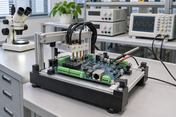
EBest Circuit can support the following inspection and testing steps:
- Bare PCB electrical testing: Checks for unintended open and short circuits against the approved netlist. Specified dimensional, hole-quality, and controlled-impedance checks can be included when required.
- Solder Paste Inspection (SPI): Verifies solder paste deposition before component placement, helping identify insufficient or excessive paste and printing misalignment.
- Automated Optical Inspection (AOI): Detects selected visible soldering defects, missing components, placement errors, and incorrect component orientation.
- X-ray inspection: Evaluates inaccessible solder joints, including suitable BGA and bottom-terminated packages where hidden-joint inspection is required.
- ICT or flying probe testing: Identifies selected electrical and assembly faults when suitable test access and an approved test program are available.
- Alarm input testing: Verifies normal, triggered, restored, open-circuit, and short-circuit conditions for applicable supervised alarm channels.
- Output and communication testing: Checks relay operation under specified loads and verifies Ethernet or RS-485 communication against the approved test procedure.
- Power and recovery testing: Measures the required power rails and current consumption, and checks startup, reset, and recovery after specified supply interruptions.
- Environmental and continuous-operation testing: Where required, evaluates operation under defined temperature, humidity, loading, or extended-running conditions.
Each functional test must have defined inputs, expected results, and pass/fail criteria. For example, an alarm input test should specify the electrical state applied to the channel and the corresponding response expected from the controller.
Passing AOI, electrical testing, and short functional tests does not automatically prove years of uninterrupted operation. 24/7 reliability requires suitable equipment-level qualification, with operating conditions and test duration established according to the actual application.
What Custom Security Monitoring PCB Manufacturing and Assembly Services Does EBest Circuit Offer?
EBest Circuit provides custom multilayer PCB fabrication, SMT/THT assembly, component sourcing, and project-specific testing for security monitoring equipment. Manufacturing follows the customer’s approved Gerber files, BOM, assembly drawings, and acceptance requirements.
Our services include:
- Custom PCB fabrication: Single-sided, double-sided, and multilayer FR-4 PCBs, including high-Tg materials and controlled-impedance constructions where applicable.
- SMT assembly: Placement and soldering of microcontrollers, communication ICs, power devices, protection components, and surface-mounted passive components.
- THT assembly: Installation of terminal blocks, relays, connectors, and other through-hole components.
- Component sourcing: Full-turnkey, partial-turnkey, and customer-consigned assembly arrangements based on approved component specifications.
- Manufacturing preparation: Review of PCB panelization, component footprints, connector orientation, soldering accessibility, and assembly documentation.
- Inspection and functional testing: Bare PCB electrical testing, assembly inspection, and customer-defined testing according to the agreed project scope.
- Prototype and production manufacturing: Support for engineering samples, pilot quantities, and repeat production orders.
Security monitoring boards frequently combine fine-pitch SMT components with mechanically loaded through-hole connectors. Coordinating these different assembly requirements helps prevent footprint conflicts, soldering problems, and unnecessary rework.
Before manufacturing, EBest Circuit offers a free DFM check to review fabrication and assembly feasibility, including trace spacing, hole structures, component footprints, and production accessibility.
Which Quality Certifications and IPC Standards Support Security Monitoring PCB Manufacturing?
ISO 9001 quality management and applicable IPC workmanship standards provide an important quality framework for security monitoring PCB manufacturing. They support controlled production documents, inspection criteria, corrective actions, and repeatable manufacturing processes.
EBest Circuit lists ISO 9001:2015 among its quality management certifications. The current certificate, covered manufacturing location, and applicable scope should be confirmed during project qualification.
Relevant requirements include:
- ISO 9001: Quality management requirements for controlled processes, documented information, supplier management, and corrective actions.
- IPC-A-600: Acceptability criteria for bare PCBs, including specified workmanship and structural characteristics.
- IPC-A-610: Acceptability criteria for electronic assemblies, including component placement and solder-joint workmanship.
- IPC-6012: Performance and qualification requirements for rigid PCBs when specified by the customer.
The applicable IPC revision, acceptance class, and inspection requirements should be established before production.
A manufacturing quality certificate does not automatically establish finished-product compliance. Security monitoring equipment may require separate electrical safety, EMC, environmental, or application-specific certification.
For projects requiring formal quality documentation, EBest Circuit can review the specified inspection records, acceptance criteria, and applicable certificate scope before order confirmation.
What Is the Lead Time for Security Monitoring PCB Manufacturing and Assembly?
Security monitoring PCB lead time depends on the layer count, fabrication specifications, component availability, assembly complexity, and testing requirements. Bare-board fabrication and PCBA assembly are separate production stages and should not be treated as one guaranteed delivery period.
EBest Circuit provides the following reference schedules for standard FR-4 prototype fabrication and general PCBA assembly.
| Production Stage | Reference Lead Time | Applicable Conditions |
|---|---|---|
| 2-Layer FR-4 PCB Prototype | 8 days | Standard bare-board fabrication |
| 4-Layer FR-4 PCB Prototype | 10 days | Standard bare-board fabrication |
| 8-Layer FR-4 PCB Prototype | 12 days | Standard bare-board fabrication |
| PCBA Assembly | Approximately 1 week | General assembly reference; material and process conditions must be confirmed |
Standard FR-4 prototype references apply to conventional specifications, including a 0.4–1.6 mm board thickness, H/H or 1 oz copper, lead-free HASL, green solder mask, and standard trace and hole requirements.
Special materials, ENIG finishes, controlled impedance, fine-line fabrication, complex through-hole assembly, and additional testing may affect the schedule.
For turnkey security monitoring PCB projects, the complete lead time must also account for material procurement, fabrication, assembly, testing, and shipping. Some activities can overlap, but production cannot proceed until the required materials and approved documents are available.
Send the Gerber files, BOM, order quantity, required delivery date, delivery location, and testing requirements to receive a project-specific production schedule.
How Much Does Security Monitoring PCB Manufacturing and Assembly Cost?
Security monitoring PCB manufacturing cost depends on PCB construction, component selection, assembly operations, testing requirements, and production quantity. A simple alarm input board will generally have a different cost structure from a multilayer controller with several communication interfaces and relay outputs.
The main cost factors are:
- PCB construction: Additional layers, special via structures, and controlled-impedance requirements increase fabrication complexity.
- Board size and panelization: Efficient panel layouts reduce material waste and unnecessary manufacturing handling.
- Copper thickness and materials: Heavy copper, high-Tg laminates, and nonstandard materials may increase processing costs.
- Component selection: Specialized communication ICs, connectors, relays, and protection devices affect sourcing costs and availability.
- Assembly operations: Double-sided SMT, through-hole soldering, programming, and coating require additional processes.
- Testing scope: Custom test fixtures, extended operation tests, and specific inspection documentation affect the total project cost.
Several manufacturing decisions can help reduce unnecessary expenses:
- Use standard FR-4 materials and surface finishes when they satisfy the electrical and environmental requirements.
- Optimize PCB dimensions and panelization without compromising mounting or connector accessibility.
- Confirm component availability before BOM release to reduce shortages and unplanned substitutions.
- Avoid unnecessary layer counts or special processes when standard fabrication can meet the specifications.
- Define functional-test requirements before production to reduce late fixture changes and repeated testing work.
For example, reducing an eight-layer PCB to six layers may lower bare-board fabrication cost, but only if the modified stackup still satisfies the routing, impedance, and mechanical requirements.
EBest Circuit can review PCB files and the BOM to identify feasible manufacturing options before quotation. Any proposed design or component changes require customer approval.
Why Choose EBest Circuit for Factory-Direct Security Monitoring PCB Manufacturing?
EBest Circuit helps security monitoring equipment manufacturers simplify production coordination, identify manufacturability problems early, and maintain consistent specifications across repeat orders.
Our factory-direct manufacturing services provide the following support:
- Fewer supplier handoffs: PCB fabrication, component procurement, assembly, and agreed testing can be coordinated through one manufacturing provider, reducing communication gaps between different suppliers.
- Earlier identification of manufacturing risks: Our free DFM check helps detect fabrication constraints, footprint mismatches, and assembly problems before production release.
- Controlled prototype-to-production transition: Approved PCB files, BOM revisions, assembly instructions, and testing requirements provide a consistent manufacturing baseline for repeat orders.
- Reduced risk of unauthorized substitutions: Alternative components and materials are reviewed against customer-approved specifications before implementation.
- Clearer quality acceptance: Applicable inspection records and agreed functional-test results help customers evaluate completed assemblies against defined requirements.
- Confidentiality protection: NDA arrangements can be established before customers provide proprietary circuit information or security hardware documentation.
For security monitoring equipment, an acceptable first prototype is only the beginning. Subsequent production orders must maintain the correct circuit revision, approved components, and required inspection criteria.
Working directly with EBest Circuit gives customers one manufacturing contact for technical clarification, production changes, and repeat-order coordination, while keeping responsibility for system architecture and firmware requirements clearly defined.
Security Monitoring PCB Manufacturing and Assembly Case Study
An EBest Circuit manufacturing project involved an 8-layer FR-4 PCB for surveillance and security equipment used in commercial and residential monitoring applications. The project provides a relevant reference for multilayer security monitoring PCB fabrication.
Project Background
The security equipment required a multilayer PCB to accommodate dense circuitry and signal transmission. The board construction needed to meet the specified material, thickness, copper, and surface-finish requirements while remaining suitable for subsequent electronic assembly.
Project Requirements and Challenges
The recorded PCB specifications included:
- PCB Layers: 8 layers
- Material: FR-4, Tg 170°C
- Finished Thickness: 1.3 mm ±10%
- Inner-Layer Copper: 1 oz
- Outer-Layer Copper: 1 oz
- Surface Finish: ENIG, specified gold thickness of 1 μin
- Solder Mask: Blue
- Silkscreen: White
- Delivery Format: Panelized PCB
The main manufacturing considerations involved fitting the required eight-layer construction within the specified thickness, maintaining multilayer registration, and applying the required copper and surface-finish specifications.
EBest Circuit’s Manufacturing Approach
The manufacturing specification established the approved high-Tg FR-4 material, copper weights, finished thickness, ENIG surface finish, and panel format.
For this multilayer construction, lamination, layer registration, hole plating, dimensional control, and surface finishing were the relevant fabrication processes.
Project Results
The documented project output was a panelized 8-layer FR-4 PCB for security equipment, with the construction and manufacturing specifications described above.
The available project information establishes the application and PCB specifications but does not include separately verified PCBA functional-test results, production yield, or field-reliability measurements. The project therefore serves as a multilayer PCB manufacturing reference rather than evidence of complete-system reliability qualification.
FAQs About Security Monitoring PCB Manufacturing and Assembly
Q1: Can EBest Circuit sign an NDA before receiving confidential PCB design files?
A1: Yes. NDA arrangements can be discussed and signed before confidential Gerber files, BOM information, schematics, or proprietary assembly documents are exchanged. Customers can specify confidentiality and document-handling requirements in the agreement.
Q2: Can customer-supplied components be used for security monitoring PCB assembly?
A2: Yes. Customer-consigned components can be used under an agreed assembly arrangement. Supplied materials should include approved manufacturer part numbers, quantities, packaging information, and relevant handling instructions. Incoming material status is reviewed before production.
Q3: What happens if an approved BOM component becomes unavailable?
A3: A replacement component must be reviewed and approved before use. The review should cover electrical ratings, package dimensions, operating temperature, and relevant functional requirements. Approved substitutions are recorded against the applicable BOM revision.
Q4: Can PCB design revisions be introduced after prototype production?
A4: Yes. Customers should provide the revised PCB data, updated BOM, assembly changes, and modified testing requirements. The new manufacturing package is reviewed before the next production release. Changes introduced after production begins may affect materials, scheduling, and cost.
Q5: Can individual PCBA serial numbers be added for traceability?
A5: Serial-number labeling and corresponding production records can be arranged when specified. Customers should define the numbering format, label position, identification method, and required traceability information before manufacturing.
Q6: Can customer firmware be programmed during PCB assembly?
A6: Firmware programming support can be arranged using approved firmware files, compatible programming equipment, instructions, and verification procedures. Firmware version control, security credentials, and access permissions should be confirmed before production.
Q7: Can conformal coating be applied to security monitoring PCB assemblies?
A7: Conformal coating can be arranged where required for protection against moisture or contamination. Customers should specify the coating material, masking areas, thickness requirements, and acceptance criteria. Connectors, test points, and electrical contacts may require masking.
Q8: How are security monitoring PCB assemblies packaged for international shipping?
A8: Packaging requirements can address ESD protection, mechanical damage, connector protection, and moisture-sensitive components. ESD bags, protective trays, moisture-barrier packaging, or individual labeling should be specified before shipment.
Q9: Can inspection documents be supplied with a PCB order?
A9: Inspection documentation can be arranged according to the agreed manufacturing requirements. Depending on the project, documents may include electrical-test records, dimensional inspection reports, certificates of conformity, or specified assembly-test results. Required documents should be identified before production.
Request a Quote for Custom Security Monitoring PCB Manufacturing and Assembly
Looking for a factory-direct security monitoring PCB manufacturer that can handle custom PCB fabrication, SMT/THT assembly, and quality testing? EBest Circuit provides manufacturing support for intrusion detection controllers, alarm monitoring boards, perimeter security equipment, and custom security communication PCBs.
Send your Gerber files, BOM, order quantity, required delivery date, delivery location, and testing requirements to sales@bestpcbs.com. EBest Circuit offers a free DFM check to identify potential fabrication and assembly issues before production and prepare a quotation based on your approved specifications.