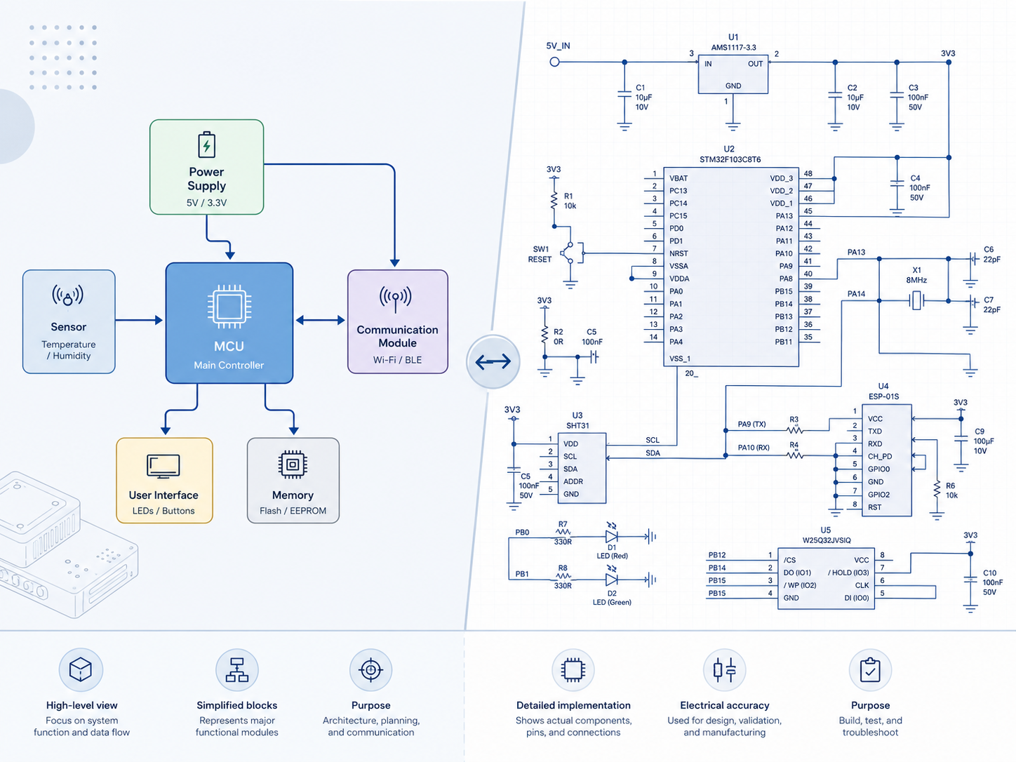
A schematic is a simplified technical drawing that shows how parts of a system connect and work together. In electronics, a schematic diagram uses standard symbols, lines, labels, and circuit numbers to explain an electrical circuit before it becomes a PCB layout, wiring harness, or finished product.
For engineers, technicians, buyers, and students, understanding schematics is a practical skill. A schematic helps you see the logic behind a circuit, identify components, trace signals, check power connections, and communicate design intent clearly. It is not only a drawing. It is the technical language behind electronic design, PCB manufacturing, troubleshooting, and assembly.

What Does Schematic Mean?
In electronics, a schematic shows components such as resistors, capacitors, ICs, connectors, diodes, transistors, switches, sensors, and power supplies. These parts are represented by symbols. Lines between the symbols represent electrical connections, also called nets.
For example, a PCB schematic may show that a microcontroller pin connects to a resistor, then to an LED, and finally to ground. The drawing may not show where those components sit on the actual circuit board. That job belongs to the PCB layout. The schematic focuses on circuit logic.
This is why a schematic is usually created before PCB layout. If the schematic is wrong, the PCB layout will also carry that mistake into production.
What Is a Schematic Also Known As?
A schematic is also known as a schematic diagram, circuit diagram, electrical schematic, electronic schematic, wiring schematic, or circuit schematic.
These names are often used in different situations:
| Term | Common Meaning | Typical Use |
|---|---|---|
| Schematic diagram | General technical drawing showing connections and functions | Electronics, machines, control systems |
| Circuit diagram | Electronic or electrical circuit drawing | PCB design, repair, education |
| Electrical schematic | Drawing for electrical power, control, or wiring logic | Industrial panels, machines, building systems |
| Electronic schematic | Drawing for electronic circuits using components and ICs | PCB, embedded systems, consumer electronics |
| Wiring schematic | Drawing focused on wire connections | Automotive, equipment wiring, cable harnesses |
| Block diagram | High-level system diagram using functional blocks | Early design, product architecture |
In PCB work, “schematic” usually means the electronic circuit drawing used to generate the netlist for PCB layout. It is closely linked with the BOM, component footprints, design rules, and assembly documentation.
Electrical Schematic Symbols and Meanings
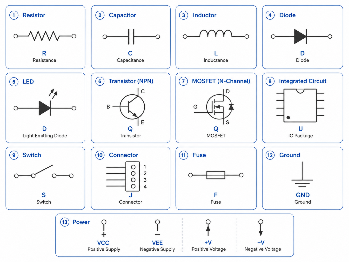
Electrical schematic symbols are standardized graphic marks used to represent components and functions. They help people read a circuit without needing a realistic picture of each part.
A resistor symbol does not look like an actual resistor body. A capacitor symbol does not show its real package size. An IC symbol may only show pin names and numbers. This simplified style makes the drawing easier to read, especially for complex circuits.
Here are common electrical schematic symbols and their meanings:
| Component or Symbol Name | Meaning in a Schematic | Common Reference Designator |
|---|---|---|
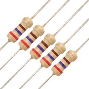
| Resistor | Limits current, divides voltage, sets bias, or provides pull-up/pull-down control | R |
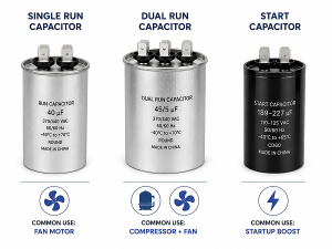
| Capacitor | Stores charge, filters noise, stabilizes voltage, or couples signals | C |
| Inductor | Stores energy in a magnetic field, filters current, or works in power circuits | L |
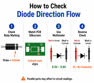
| Diode | Allows current flow mainly in one direction | D |
| LED | Emits light when current flows in the forward direction | LED or D |
| Zener diode | Provides voltage regulation or overvoltage protection | ZD or D |
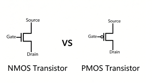
| Transistor | Switches or amplifies signals | Q |
| MOSFET | Switches power or controls current flow | Q |
| Integrated circuit | Performs logic, control, power conversion, memory, or signal processing | U or IC |
| Connector | Provides an interface to cables, modules, power, or external systems | J, CN, or P |
| Switch | Opens or closes a circuit path | SW or S |
| Fuse | Protects a circuit by opening under excessive current | F |
| Ground | Common reference point for voltage and return current | GND |
| Power symbol | Shows supply voltage such as 3.3V, 5V, 12V, or VCC | VCC, VIN, VDD |
| Test point | Place for measurement during debugging or production testing | TP |
| Crystal or oscillator | Provides a clock signal for ICs or microcontrollers | Y or X |
Symbols may vary slightly depending on the standard, software, region, or industry. For PCB projects, the symbol must also match the correct footprint. A correct schematic symbol with the wrong footprint can still cause assembly failure.
For example, a capacitor may be electrically correct in the schematic, but if its footprint does not match the real package, the part may not fit during SMT assembly. This is a common DFM issue in PCB manufacturing.
What Do the Circuit Numbers Shown on Schematics Usually Mean?
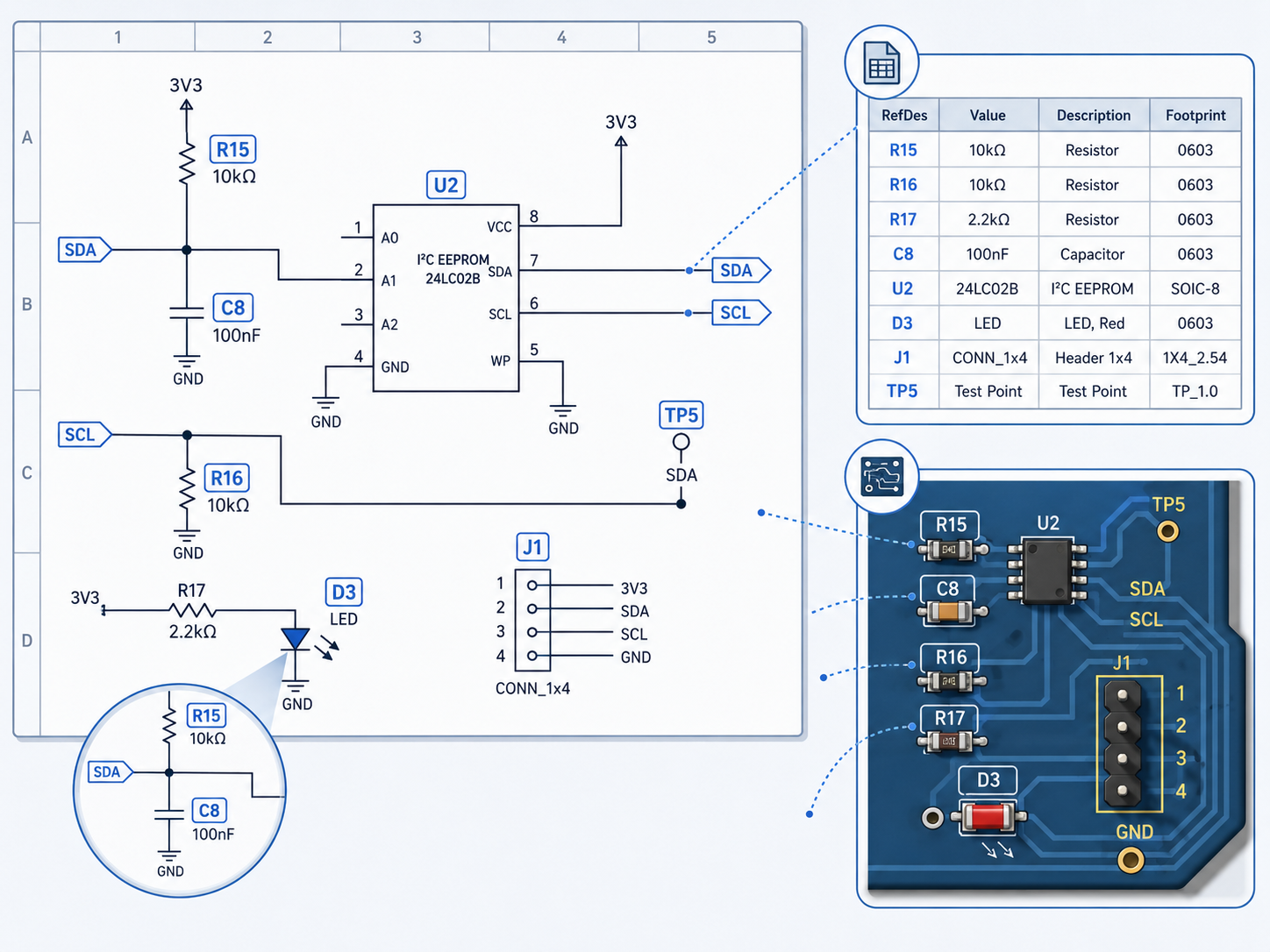
The circuit numbers shown on schematics usually identify components, pins, wires, nets, pages, and functional sections. They help engineers, assemblers, and repair technicians locate the same item across the schematic, PCB layout, BOM, silkscreen, and test documents.
The most common numbers are reference designators. Examples include R1, R2, C1, U3, D5, J1, and TP2.
Here is what they usually mean:
| Example | Meaning |
|---|---|
| R15 | The fifteenth resistor listed in the design |
| C8 | The eighth capacitor listed in the design |
| U2 | The second IC or module listed in the design |
| D3 | The third diode or LED listed in the design |
| J1 | The first connector listed in the design |
| TP5 | The fifth test point listed in the design |
| Pin 1, Pin 2 | Physical or logical pin numbers on a component |
| Net labels such as SDA, SCL, GND | Names of electrical connections |
| Sheet numbers | Page references in multi-page schematics |
These numbers are important because they connect the design file to real production work. When a BOM says “R15 = 10kΩ, 1%, 0603,” the assembly team knows exactly which resistor to place at R15 on the PCB. When a technician checks a failed board and sees U2 overheating, the schematic helps identify what U2 does and which power rail feeds it.
What Is an Example of a Schematic?
A simple example of a schematic is an LED indicator circuit. In this circuit, a power source connects to a resistor. The resistor connects to an LED. The LED connects to ground. When voltage is applied, current flows through the resistor and LED, so the LED lights up.
The schematic may include:
- VCC or 5V power symbol
- R1 resistor
- D1 LED
- GND symbol
- Connection lines between them
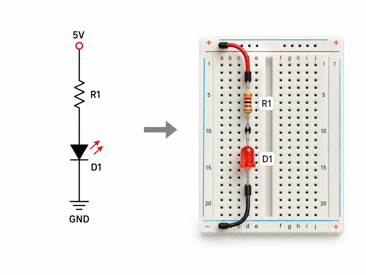
In PCB manufacturing, this schematic later becomes part of the full design package. The PCB factory mainly uses Gerber files, drill files, stack-up, BOM, Pick-and-Place files, and assembly drawings, but the schematic is still valuable during engineering review, functional discussion, debugging, and DFM checks.
What Are the Two Types of Schematics?
There is no single universal answer because different industries classify schematics in different ways. In electronics and electrical engineering, two common types are electrical schematics and electronic schematics.
An electrical schematic often focuses on power distribution, control circuits, motors, relays, switches, breakers, terminals, and wiring paths. It is common in industrial equipment, automation panels, HVAC systems, vehicles, and building electrical systems.
An electronic schematic focuses on electronic components such as ICs, resistors, capacitors, diodes, MOSFETs, sensors, oscillators, connectors, and signal networks. It is common in PCB design, embedded systems, medical electronics, consumer devices, automotive control modules, communication devices, and power electronics.
What Is the Difference Between Blueprints and Schematics?
Blueprints and schematics are both technical drawings, but they serve different purposes.
A blueprint usually shows physical construction details. It focuses on dimensions, location, shape, structure, installation, and building or manufacturing instructions. Blueprints are common in architecture, mechanical design, construction, and product fabrication.
A schematic shows functional relationships. It focuses on how parts connect and work together. In electronics, it shows the electrical logic of a circuit, not the final physical position of every component.
| Item | Blueprint | Schematic |
|---|---|---|
| Main purpose | Shows physical structure and dimensions | Shows functional connections and circuit logic |
| Common industries | Construction, architecture, mechanical design | Electronics, electrical systems, automation |
| Level of physical detail | High | Usually low |
| Shows actual size or scale | Often yes | Usually no |
| Shows electrical logic | Not usually | Yes |
| Used for PCB design | Less common | Essential before PCB layout |
For PCB projects, the closest equivalent to a blueprint is the PCB layout or fabrication drawing. It shows board dimensions, hole sizes, layer stack-up, copper layers, solder mask, silkscreen, and manufacturing details. The schematic, however, shows the circuit logic behind that board.
What Are Schematics Used For?
Schematics are used to design, explain, verify, repair, and manufacture electrical or electronic systems. They act as a shared technical language between engineers, technicians, manufacturers, and customers.
In electronics, schematics are used for:
- Circuit design
- PCB layout preparation
- Component selection
- BOM creation
- Signal tracing
- Power rail review
- Design verification
- Debugging and repair
- Functional testing
- Engineering communication
- Product documentation
- Manufacturing support
For PCB and PCBA projects, schematics help detect issues before production. For example, an engineer may review whether pull-up resistors are missing, whether decoupling capacitors are placed on the correct power pins, whether connector pinouts match the cable, or whether power nets are named clearly.
Who Uses Schematics?
Schematics are used by many people across the product lifecycle. The same drawing may support concept design, PCB layout, manufacturing, testing, repair, and product improvement.
Common users include:
Electrical engineers use schematics to design power, control, and signal circuits.
Electronics engineers use schematics to create PCB-based products, embedded systems, power supplies, sensor boards, and communication modules.
PCB layout engineers use schematics to generate netlists and route the PCB correctly.
Firmware engineers use schematics to understand microcontroller pins, communication buses, reset circuits, boot modes, and debugging interfaces.
Manufacturing engineers use schematics to check test points, assembly risks, and production test logic.
Repair technicians use schematics to trace faults, measure voltages, and identify failed parts.
Quality engineers use schematics during failure analysis and process improvement.
Procurement teams may not design the circuit, but they use schematic-related data to understand BOM risk, part alternatives, and supplier communication.
Students and hobbyists use schematics to learn circuits and build projects.
In professional PCB manufacturing, a schematic is not always enough for quotation or production. A complete package usually includes Gerber files, drill files, BOM, Pick-and-Place files, PCB stack-up, assembly drawings, impedance requirements, and testing requirements. Still, the schematic remains one of the most important documents for understanding the design.
What’s the Difference Between a Diagram and a Schematic?
A diagram is a broad term. It can mean any drawing that explains information visually. A schematic is a specific kind of diagram that uses symbols and connections to show how a system works.
All schematics are diagrams, but not all diagrams are schematics.
For example, a flowchart is a diagram. A product exploded view is a diagram. A wiring map is a diagram. A PCB layout image is also a diagram in a general sense. But an electronic schematic is more specific because it follows circuit logic and uses electrical symbols.
| Item | Diagram | Schematic |
|---|---|---|
| Meaning | General visual explanation | Symbol-based functional drawing |
| Scope | Broad | More specific |
| Can show physical shape | Yes | Usually simplified |
| Uses technical symbols | Sometimes | Usually yes |
| Common examples | Flowchart, block diagram, layout, map | Circuit schematic, electrical schematic |
| Main goal | Explain visually | Show how parts connect and function |
A diagram may help someone understand an idea. A schematic helps someone build, test, or repair a system.
For PCB design, the difference is important. A product diagram may show where the board fits inside a device. A PCB layout shows component placement and routing. A schematic shows the electrical relationships that make the product work.
FAQs About Schematics Meaning
What does schematics mean in simple words?
Schematics means technical drawings that show how parts of a system connect and work together. In electronics, schematics use symbols to represent components such as resistors, capacitors, ICs, switches, connectors, and power sources. The drawing does not focus on physical appearance. It focuses on function and connection.
What is the meaning of a schematic diagram?
A schematic diagram is a simplified drawing that explains the structure or logic of a circuit, machine, or system. In an electrical or electronic schematic, symbols represent components, and lines represent connections. It helps engineers and technicians understand how current, signals, or control functions move through the design.
Are schematic diagrams and circuit diagrams the same?
In electronics, the terms are often used in the same way. A circuit diagram is a type of schematic diagram that shows electronic or electrical connections. However, “schematic diagram” can be broader. It may also describe hydraulic, mechanical, pneumatic, or system-level drawings in other industries.
Why are schematic symbols important?
Schematic symbols make complex circuits easier to read. Instead of drawing real component shapes, the schematic uses standard symbols that engineers can recognize quickly. This saves space, improves clarity, and reduces misunderstanding. Symbols also help connect the schematic to the BOM, PCB layout, testing process, and repair work.
Do schematics show the real location of components?
Usually, no. A schematic shows electrical connections and circuit logic, not the actual physical placement of parts. The PCB layout shows real component locations, copper traces, vias, board outline, and layer structure. Both documents are needed, but they answer different questions.
What do R, C, U, D, and J mean on a schematic?
These letters are reference designators. R usually means resistor, C means capacitor, U means integrated circuit, D means diode, and J often means connector. The number after the letter identifies the specific part, such as R1, C5, U2, or J3. These labels help match the schematic, BOM, PCB silkscreen, and assembly files.
Can a PCB be made from a schematic only?
A schematic alone is usually not enough for PCB fabrication. The manufacturer needs Gerber files, drill files, board specifications, stack-up, copper thickness, surface finish, solder mask color, and other fabrication details. For PCBA, the BOM and Pick-and-Place file are also needed. The schematic is useful for understanding and checking the circuit.
What is the difference between a schematic and a wiring diagram?
A schematic focuses on circuit function and logical connections. A wiring diagram focuses more on real wire connections, terminals, harnesses, and installation paths. In electronics, schematics are common for PCB design. Wiring diagrams are more common in automotive systems, industrial control cabinets, machines, and field installation work.
How do beginners read a schematic?
Start by finding the power input, ground symbols, and main functional blocks. Then identify key components such as ICs, connectors, regulators, sensors, and switches. Follow net labels and signal names instead of only following lines. Read reference designators and component values carefully. For complex circuits, study one section at a time.
Why do PCB manufacturers sometimes need schematics?
PCB manufacturers may request schematics during engineering review, PCBA debugging, functional testing, or DFM discussion. The schematic helps explain design intent, signal flow, power rails, connector functions, and test points. It is especially useful for complex boards involving impedance control, power circuits, RF sections, mixed-signal design, or turnkey assembly.
Conclusion
For PCB and PCBA projects, a clear schematic reduces design errors, improves communication, supports better layout work, and makes testing or troubleshooting much easier. Before moving from design to manufacturing, it is worth checking that the schematic, BOM, footprints, net names, connector pinouts, and PCB layout all match correctly.
If you’re sourcing reliable PCB/PCBA manufacturing — OEM, ODM, prototyping, mass production, or custom engineering solutions — reach out to our engineering team for technical support and a quote at sales@bestpcbs.com.