





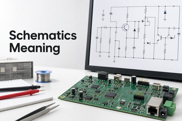
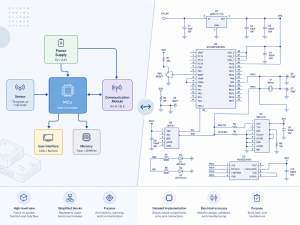
schematics meaning refers to simplified technical drawings that show components and their electrical connections with symbols rather than realistic pictures. In electronics, a schematic explains how a circuit is intended to work. It does not show the physical size or exact board position of every part.
A useful schematic lets a designer follow power, signals, control paths, and component relationships before those connections become copper traces on a PCB. This guide explains the notation, the reading sequence, and the checks that matter when a design moves toward fabrication and assembly.
What Does a Schematic Show?
A schematic shows electrical relationships: which pins connect, how power reaches each circuit block, and how signals move between components. Its basic elements are symbols, wires, junctions, net labels, power symbols, and notes.
The drawing is logical rather than physical. A resistor shown beside an IC may sit several centimeters away on the finished board. Conversely, two symbols placed far apart on a schematic may connect through a shared net label without a long line between them.
- Symbols identify component functions.
- Wires and junctions show direct electrical connections.
- Net labels connect points that share the same named signal.
- Power and ground symbols identify supply networks and reference nodes.
- Reference designators link each schematic symbol to a specific component.
What Is the Schematic Diagram Meaning in Electronics?
The schematic diagram meaning in electronics is a functional map of a circuit. It tells the reader what connects to what and why each component is present, but it usually leaves mechanical placement and routing to the PCB layout.
For example, a power-supply section may show an input connector, protection device, regulator, input and output capacitors, and a ground return. The schematic makes the intended electrical sequence clear even though the actual components may be arranged differently to control heat, noise, and trace length.
Readers who want another practical walkthrough can also review how to understand circuit diagrams.
What Does Electrical Schematics Meaning Cover?
Electrical schematics meaning covers the symbolic representation of electrical circuits, power distribution, controls, and interconnections. In an electronics project, it normally includes component symbols, pin numbers, signal names, supply rails, ground references, and notes about values or part choices.
The same principle applies from a small sensor board to a larger control system. The drawing reduces a complex assembly to relationships that can be reviewed, simulated, tested, and transferred into PCB design software.
A schematic can also support several downstream tasks:
- Electrical rule checking before layout
- Component annotation and BOM generation
- Footprint assignment for PCB layout
- Signal tracing during bring-up and repair
- Design review between hardware, layout, firmware, and production teams
What Do Common Schematic Symbols Mean?
Schematic symbols represent component functions with standardized graphical forms. The exact artwork can vary between IEC and ANSI conventions, but the electrical role remains recognizable when the drawing is prepared correctly.
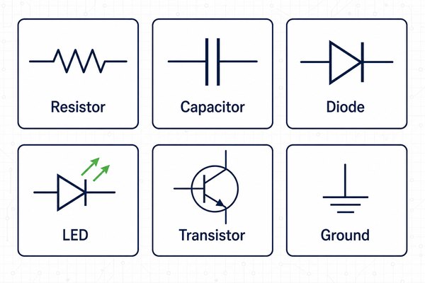
| Symbol | Typical function | Common designator |
| Resistor | Limits current, divides voltage, or sets bias | R |
| Capacitor | Stores charge, filters noise, or couples signals | C |
| Diode | Controls current direction or protects a circuit | D |
| Transistor | Switches or amplifies an electrical signal | Q |
| Integrated circuit | Combines a defined electronic function in one package | U |
| Connector | Provides an electrical interface to another board or cable | J or CN |
The search phrase schematics symbols meaning usually reflects a need to identify both the graphic and its function. Do not rely on shape alone. Confirm the designator, component value, pin names, polarity marks, and the symbol library standard used in the project.
How Do Reference Designators and Values Work?
Reference designators give every component a unique identity. The letter identifies the component class, while the number distinguishes one instance from another. R12 is a particular resistor; C7 is a particular capacitor; U3 is a particular integrated circuit.
The text near a symbol may contain several different fields:
- Reference: the unique identifier, such as R12 or U3
- Value: the resistance, capacitance, part number, or functional value
- Pin name or number: the electrical terminal used by the connection
- Footprint: the PCB land pattern assigned to the component
- Part data: manufacturer number, tolerance, voltage rating, or other controlled fields
Designators must stay consistent across the schematic, BOM, PCB layout, assembly drawing, and inspection records. A mismatch can place the correct part at the wrong location or make troubleshooting unnecessarily difficult.
How Do Nets, Junctions, and Signal Flow Work?
Nets are electrically connected groups of pins and conductors. A drawn wire creates a visible connection, while identical net labels can connect distant points without drawing a continuous line across the page.
A junction dot normally confirms that crossing wires connect. Lines that cross without a junction may remain electrically separate, depending on the drafting convention and software. This is one reason a visual glance is not enough; the design should also pass an electrical rules check.
Read signal flow by blocks rather than by every line at once:
- Locate the power input and ground reference.
- Identify connectors, sensors, switches, or other input sources.
- Follow named nets into processing, control, or amplification blocks.
- Trace outputs to loads, connectors, indicators, or communication interfaces.
- Check feedback, enable, reset, and protection paths separately.
How Is a Schematic Different from a Wiring Diagram?
A schematic emphasizes circuit logic, while a wiring diagram emphasizes physical connections, terminals, wire colors, cable paths, or installation details. The two documents may describe the same system, but they answer different questions.
The phrase wiring schematics meaning is often used loosely. A wiring schematic may combine logical symbols with connector and wire information, while a detailed harness drawing can add wire gauge, color, length, crimp terminal, and pin-location data.
| Document | Primary purpose | Shows physical placement? |
| Schematic | Explains electrical logic and connectivity | Usually no |
| Wiring diagram | Guides point-to-point connection or installation | Sometimes |
| PCB layout | Defines footprints, copper, holes, and board geometry | Yes |
| Assembly drawing | Shows component locations and orientation | Yes |
How Is a Schematic Different from a PCB Layout?
A schematic defines logical connectivity; a PCB layout defines the physical implementation of that connectivity. Layout adds board outline, component footprints, placement, copper routing, vias, planes, clearances, and mechanical constraints.
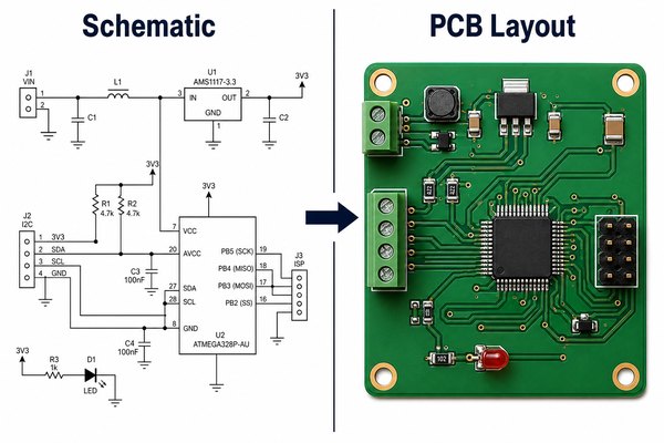
The netlist transfers electrical connections from the schematic into the board environment. The layout designer then decides where parts sit and how traces reach them while managing return paths, noise, heat, manufacturability, and assembly access.
If you are moving from circuit concept to a board, this guide on how to design a PCB board explains the broader workflow.
How Should You Read an Electronic Schematic Step by Step?
Start with the circuit purpose, then read one functional block at a time. Trying to follow every wire from the upper-left corner often hides the design intent.
- Read the title block and notes. Confirm document revision, sheet count, design variant, and stated assumptions.
- Find power entry and regulation. Identify input protection, voltage rails, decoupling, and ground domains.
- Divide the drawing into blocks. Mark input, processing, memory, communication, driver, and output sections.
- Trace one important signal. Follow its net labels and pin connections across sheets.
- Check component context. Read values, polarity, ratings, and the relationship to nearby parts.
- Match designators to the PCB. Use the placement or assembly view when physical location matters.
- Check abnormal paths. Review reset, enable, feedback, fault, protection, and programming connections.
For a board-level example, see how to read circuit boards and schematics together.
Which Schematic Errors Can Become PCB Problems?
Schematic errors become PCB problems when incorrect connectivity or incomplete component data transfers into layout. Some mistakes stop a board from operating; others create intermittent faults that appear only under load, temperature, or electromagnetic stress.
- Unconnected or incorrectly labeled power pins
- Missing pull-up, pull-down, bias, or decoupling components
- Reversed diode, LED, capacitor, or connector polarity
- Swapped connector pin numbers
- Duplicate reference designators
- Wrong component value, rating, or footprint assignment
- Net labels that differ by a character, space, or hierarchy level
- Hidden power connections that mask the intended current path
- Functional blocks copied without updating addresses or control pins
Electrical rule checking can catch many connection and pin-type conflicts, but it cannot judge every design decision. A human review still needs to confirm operating conditions, datasheet requirements, interface assumptions, and failure behavior.
How Can a Schematic Help with PCB Troubleshooting?
A schematic gives troubleshooting a logical starting point. Instead of probing components at random, a technician can identify the expected power rail, signal source, protection device, control node, and load, then test the circuit in that sequence.
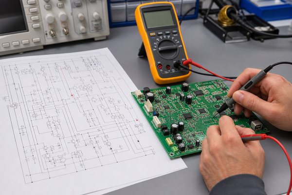
Use reference designators to match a schematic component to the board. Then compare measured voltages or waveforms with the expected function of that block. When the symptom is a short or an open connection, this article on how to test for an open or short circuit on a PCB provides a related diagnostic path.
What Documents Are Needed After the Schematic Is Complete?
A schematic alone is not normally enough to manufacture and assemble a PCB. Fabrication needs board-production data, while assembly needs accurate component and placement information.
- Gerber or ODB++ data: copper, solder mask, silkscreen, and board outline
- Drill data: plated and non-plated hole definitions
- BOM: designators, quantities, values, packages, and approved part numbers
- Pick-and-place file: component coordinates, rotation, and board side
- Assembly drawing: orientation and special placement instructions
- Test requirements: test points, programming steps, limits, and acceptance criteria
The schematic remains important because it explains intent when a file conflict or technical question appears. However, the manufacturer builds the physical board from production data such as PCB Gerber files, not from a schematic screenshot.
FAQ About Schematics Meaning
What is the simple definition of a schematic?
A schematic is a simplified technical drawing that uses symbols and lines to show how parts of a system connect or interact. In electronics, it represents components, pins, nets, power, and signal relationships.
What is a schematic example?
A basic LED circuit is a schematic example. It can show a power source, current-limiting resistor, LED, switch, and ground connected in the intended electrical order.
What are schematics used for?
Schematics are used to design circuits, review connectivity, run electrical checks, assign footprints, support PCB layout, generate a BOM, and troubleshoot assembled hardware.
Is a schematic the same as a blueprint?
No. A schematic focuses on functional relationships and may ignore physical scale. A blueprint or production drawing generally provides dimensions, placement, construction, or manufacturing details.
Is a schematic the same as a circuit diagram?
In electronics, the terms are often used interchangeably. Both normally describe a symbolic drawing of circuit components and electrical connections.
Does a schematic show component locations?
Usually not. A schematic groups components to explain circuit function. The PCB layout and assembly drawing show the physical positions and orientations.
What do letters and numbers mean on a schematic?
Letters and numbers form reference designators. R indicates a resistor, C a capacitor, D a diode, Q a transistor, U an integrated circuit, and J or CN a connector. The number identifies the individual component.
Why do identical net labels appear in different places?
Matching net labels create the same logical electrical connection without drawing a long wire across the page. Their scope may be local, global, or hierarchical, depending on the design software and project structure.
Do all schematic symbols look the same?
No. Symbol shapes can vary between standards, libraries, regions, and software. The component function, pin names, designator, and surrounding circuit help confirm the intended meaning.
Can a PCB manufacturer build a board from only a schematic?
Not usually. The schematic explains the electrical design, but PCB fabrication requires board-production files. Assembly also needs a BOM and placement data. Missing files must be completed before reliable production can begin.
How Can EBest Circuit Move a Schematic Toward Production?
EBest Circuit can review a schematic together with the PCB production package to clarify connectivity, component data, and manufacturing requirements before fabrication or assembly. A complete package should include the schematic, Gerber or ODB++ data, drill files, BOM, pick-and-place data, quantities, and any test instructions.
Use this schematics meaning guide as a pre-handoff reference, then submit the controlled design files for an engineering review and quotation.
You may also like







Tags: electrical schematics meaning, schematic diagram meaning, schematics meaning, schematics symbols meaning, wiring schematics meaning