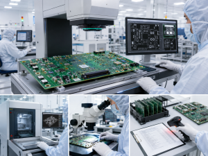
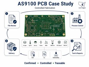
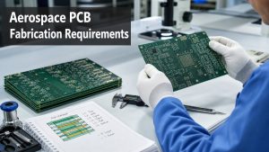
Satellite PCB assembly services turn your approved design into assembled, inspected, and tested boards for satellite electronics. High reliability depends on suitable materials, sound solder joints, cleanliness, and mechanical support. Full traceability connects delivered boards to their components, build revisions, production history, and test results.
At EBest Circuit, a dedicated engineering team coordinates PCB fabrication, component sourcing, assembly, and agreed testing. Before production, we review your files, identify manufacturing concerns, and confirm component availability and inspection requirements, helping you prepare for system integration with fewer unresolved assembly questions.

What Is Satellite PCB Assembly?
Satellite PCB assembly is the process of mounting and soldering electronic components onto a printed circuit board to create a functional assembly for satellite electronics. It establishes the electrical connections between components that allow the board to perform its intended function.
Where Are Satellite PCB Assemblies Used?
Satellite PCB assemblies support onboard computing, communications, power distribution, attitude control, and payload operation.
| Application | Electronic Function | Assembly Priorities |
|---|---|---|
| Onboard computers | Command processing, data handling, and storage | Fine-pitch joints, memory placement, programming, and connectors |
| Communication modules | Command reception, telemetry, and RF transmission | RF components, shielding, grounding, and connector installation |
| Power systems | Voltage conversion, protection, and distribution | High-current joints, thermal paths, and load testing |
| Attitude-control electronics | Sensor acquisition and actuator control | Sensor orientation, component retention, and interface checks |
| Payload electronics | Imaging, measurement, sensing, and processing | Dense packaging, cleanliness, mechanical fit, and functional testing |
A communication board may require inspection of RF connectors and shielding connections. A power board may need closer attention to large solder joints, heat distribution during assembly, and performance under specified loads.
What Are the Reliability Requirements for Satellite PCB Assembly?
Satellite PCB assembly requires dependable connections, compatible materials, secure components, and workmanship suited to the mission environment.
- Launch vibration and shock: Connectors, larger components, and unsupported structures can transfer mechanical loads into solder joints. Design-specified staking, fastening, or supports help manage these stresses.
- Temperature changes: Packages and PCB materials expand at different rates, placing stress on connections. Material selection, package geometry, solder joint formation, and the expected temperature range must work together.
- Vacuum compatibility: Laminates, adhesives, coatings, labels, and process residues must satisfy the project’s material and contamination requirements.
- Long operating periods: Stable connections, suitable handling, and consistent assembly support service-life requirements alongside design validation and qualification.
Cleanliness is especially important near contamination-sensitive equipment. Material selection, cleaning, and curing must address applicable contamination and outgassing requirements. sma.nasa.gov
Radiation requirements influence component selection and circuit design. The assembly service should preserve those decisions through approved parts, handling instructions, and substitution controls.
Specify the workmanship standard, revision, acceptance criteria, and additional space-hardware requirements before production.
How Are PCB Materials and Components Selected for Satellite PCB Assembly?
Materials and components are selected according to electrical performance, temperature exposure, mechanical demands, and project qualification requirements.
PCB materials and construction
Laminate selection considers thermal expansion, dielectric performance, moisture behavior, and compatibility with assembly temperatures. High-Tg FR-4, polyimide, and low-loss materials serve different needs; the choice should follow the board’s requirements.
Stackup and copper distribution also affect assembly. Heavy copper and large ground connections draw heat away from soldering locations, while thin boards may need support during printing, placement, or reflow.
Components and approved sources
The BOM should identify manufacturer part numbers, packages, approved alternatives, and sourcing or screening restrictions. Include required lot information and documentation for critical devices.
Moisture-sensitive components need appropriate storage and preparation. Customer-supplied parts should arrive with sufficient packaging and exposure-history information to determine their handling requirements.
Soldering and post-processing materials
Surface finishes, solder alloys, fluxes, cleaners, adhesives, and coatings must be compatible. Their combination affects wetting, residue removal, curing, inspection, and repair.
Outgassing data can assist spacecraft material evaluation, with suitability assessed against the project’s application and conditions.
Review alternatives beyond footprint compatibility. Ratings, finish, thermal behavior, firmware dependencies, and qualification history can affect whether a substitute is acceptable.
How Does DFM Review Improve Satellite PCB Assembly Reliability?
DFM review identifies manufacturing problems before they lead to defective assemblies, purchased-material losses, or production delays.
- File inconsistencies: Conflicting BOMs, drawings, placement data, or PCB revisions can result in incorrect components or orientations.
- Soldering difficulties: Pad dimensions, paste openings, spacing, and uneven thermal connections can contribute to bridging, insufficient solder, or component movement.
- Handling concerns: Board thickness, edge-mounted parts, panel features, and depaneling clearance affect assembly stability and damage risk.
- Limited inspection access: Shields, tall components, and restricted test points can obstruct important checks.
For example, a connector too close to a panel edge may interfere with tooling. Identifying the conflict before fabrication allows your team to adjust the design or agree on suitable tooling.
Each finding should identify the affected location, explain the concern, and provide an actionable recommendation. Approved changes should then appear in the files used for production.
What Is the Satellite PCB Assembly Process?
Satellite PCB assembly follows a sequence of engineering review, material preparation, placement, soldering, post-processing, and verification.
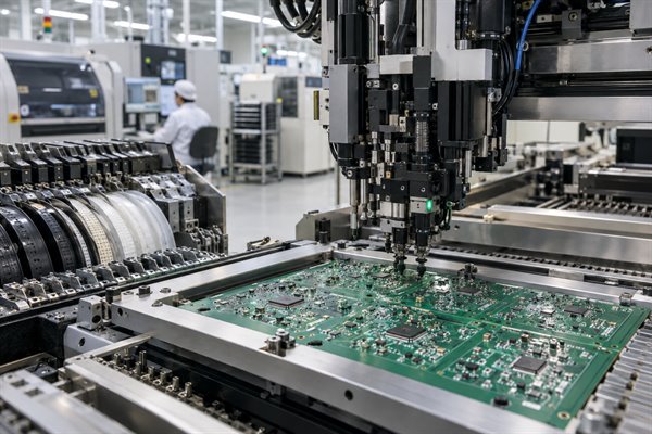
- Manufacturing-file review PCB files, the BOM, placement data, drawings, and special requirements are checked. Manufacturing questions are returned for clarification before preparation proceeds.
- Material verification PCB and component identity, condition, quantities, and documentation are inspected. Shortages, discrepancies, and proposed substitutions require resolution.
- Production preparation Stencils, placement programs, supports, and instructions are prepared against the approved revision. Moisture-sensitive materials receive the required handling.
- Paste printing and placement Paste deposits and initial placements are checked as specified. First-piece inspection confirms component identity, polarity, orientation, and critical positions.
- Soldering and mixed assembly SMT components follow the approved reflow process. Through-hole components and connectors are installed using the selected soldering method.
- Post-processing Required cleaning, staking, coating, hardware installation, and programming follow the assembly instructions, preserving access for intermediate checks.
- Final inspection and delivery Boards complete the agreed inspections and tests. Defects are resolved, relevant checks are repeated after repair, and accepted assemblies are packaged with the specified records.
How Are Satellite PCB Assemblies Inspected and Tested?
Inspection checks manufacturing quality; electrical and functional testing verify specified circuit behavior. Your plan should cover critical connections and functions before integration restricts access.
Solder paste inspection
SPI measures specified paste characteristics, such as volume and alignment, before placement. It helps detect printing conditions that may cause bridging or insufficient solder.
AOI and visual inspection
AOI examines accessible features, including placement, polarity, and visible solder conditions. Visual inspection supports checks of connectors, hardware, handling damage, staking, and coating.
X-ray inspection
X-ray examines selected hidden solder features beneath packages such as BGAs and QFNs. Define inspected locations, acceptance criteria, and required image records.
Electrical and functional testing
ICT or flying probe can check accessible connections and selected component values. Functional testing applies specified firmware, power, signals, and loads.
A power board may be checked for output voltage and protection response. A controller may be tested for startup, communications, and sensor interfaces.
Results should identify the tested board or batch and show the applicable limits and outcomes. After repair, repeat the inspections and tests affected by the work.
How Is Full Traceability Maintained Throughout Satellite PCB Assembly?
Full traceability links each delivered board or batch to its design revision, materials, manufacturing history, verification results, and approved changes.
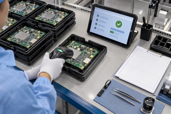
Records connect through work orders, batch numbers, or individual serial numbers. The required detail depends on your hardware and acceptance needs.
- Build identity: PCB revision, BOM revision, assembly drawings, and firmware version.
- Material history: PCB manufacturing batch, component part numbers, and required supplier or lot information.
- Production history: Relevant instructions, program identification, and completion records for specified operations.
- Verification results: Inspection reports, X-ray records, electrical measurements, and functional-test results.
- Changes and repairs: Approved substitutions, deviations, affected units, repair details, and retest results.
If a component lot requires investigation, these links help identify the assemblies containing it. If a unit fails testing, its history supports comparison with other boards.
Agree on record contents, product identification, delivery format, and retention period before production.
What Affects Satellite PCB Assembly Cost and Lead Time?
Cost and lead time depend on PCB construction, component availability, assembly complexity, testing, and documentation.
Board construction and assembly
Materials, layer count, copper thickness, vias, finish, and tolerances affect fabrication cost. Fine-pitch parts, double-sided assembly, mixed technologies, coating, and mechanical installation can add preparation and processing time.
Component supply
Long-lead devices, approved-source restrictions, screening, and minimum purchase quantities affect procurement. An early BOM review helps you identify schedule constraints and consider approved alternatives.
Testing and records
Fixtures, programming adapters, functional-test development, additional inspection, serialization, and reporting require separate preparation. Their inclusion should be visible in the quotation.
Order quantity
Stencils, tooling, and engineering setup contribute more to the unit price of a small initial build. Repeat orders may reuse suitable preparation when the design and requirements remain consistent.
Compare quotations using the same materials, processes, tests, records, and packaging. Delivery estimates should reflect component readiness and completion of the required tooling and test inputs.
Why Choose EBest Circuit as Your Satellite PCB Assembly Manufacturer?
EBest Circuit coordinates PCB fabrication, sourcing, assembly, and engineering support through a dedicated project team.
- Resolve manufacturing concerns early: File review identifies package, panel, and assembly issues while your team can still make practical changes.
- Coordinate PCB and PCBA requirements: Fabrication and assembly needs are reviewed together, reducing mismatched assumptions about materials, mechanical features, and files.
- Retain control over component changes: Procurement follows the approved BOM and sourcing requirements, with proposed alternatives submitted through the agreed approval process.
- Verify critical board features: Inspection and testing can address hidden joints, connectors, power sections, and specified functions.
- Plan the records needed for acceptance: Traceability and reporting requirements are discussed before production and included in the agreed delivery.
- Simplify technical communication: Engineers familiar with your project help resolve questions across purchasing and manufacturing.
Looking for a satellite PCB assembly partner? Send your Gerber files, BOM, assembly drawings, quantities, and reliability and traceability requirements to sales@bestpcbs.com. EBest Circuit’s engineering team can review manufacturing needs, component availability, and inspection and testing requirements before preparing a quotation.
What Files Are Needed for a Satellite PCB Assembly Quote?
Provide PCB manufacturing data, the BOM, placement files, assembly drawings, quantities, and test requirements.
- Board and assembly files: Gerber or ODB++, drill data, fabrication drawings, stackup, BOM, pick-and-place data, and assembly drawings.
- Manufacturing requirements: Materials, workmanship specifications, cleaning, coating, staking, mechanical installation, and traceability.
- Programming and testing: Firmware, programming method, procedures, operating conditions, pass/fail limits, fixtures, and required reports.
- Order details: Hardware purpose, quantities, target delivery, customer-supplied materials, packaging, and destination.
Contact EBest Circuit for a satellite PCB assembly quote. Send your Gerber files, BOM, assembly drawings, quantities, and testing and traceability requirements to sales@bestpcbs.com. Our engineering team will review your manufacturing needs and component availability to prepare a project-specific quotation.
FAQ About Satellite PCB Assembly
Q1: Can an NDA be arranged before complete design files are shared?
A1: Request NDA review before disclosure so confidentiality terms can be agreed before detailed files are exchanged.
Q2: Can several population variants be included in one order?
A2: Yes, provided each variant has clearly identified BOM, placement, assembly, and test requirements.
Q3: What happens to unused customer-supplied components?
A3: Return, storage, or disposal arrangements should be agreed before production begins.
Q4: Can packaging protect sensitive connectors or protruding components?
A4: Packaging can be specified around the assembly’s mechanical features, handling needs, and transport requirements.
Q5: Can part of an order be delivered before the remaining quantity?
A5: Staged delivery can be evaluated against material readiness, production scheduling, and completion of the required acceptance checks.
Q6: Does requesting a quotation commit the project to production?
A6: A quotation supports technical and commercial evaluation, with production proceeding after order acceptance and manufacturing release.