A Rogers RO3010 PCB is usually considered when an RF circuit needs a high dielectric constant, compact transmission-line structures, and predictable microwave performance. Its design Dk of 11.2 can reduce the physical size of antennas, filters, resonators, and matching networks. That advantage comes with tighter fabrication demands: narrow conductors, dielectric thickness variation, copper profile, and etching tolerance can all move the finished circuit away from its simulated response.
RO3010 is therefore a deliberate engineering choice, not a universal upgrade from FR4 or a lower-Dk Rogers material. This guide explains its properties, selection boundaries, stackup options, manufacturing challenges, testing requirements, and price factors. EBest Circuit supports Rogers PCB fabrication, Rogers/FR4 hybrid structures, controlled impedance, and prototype-to-production review through its facilities in China and Vietnam.
What Is a Rogers RO3010 PCB?
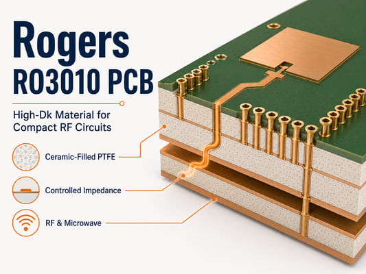
Rogers RO3010 is a ceramic-filled PTFE laminate in the RO3000 series. After copper cladding, imaging, drilling, plating, surface finishing, and other fabrication processes, it becomes the dielectric foundation of a high-frequency printed circuit board.
The RO3010 dielectric constant is its most distinctive property. A higher Dk shortens the guided wavelength, allowing resonators, filters, matching networks, and antenna elements to occupy less board area. This makes RO3010 useful when RF circuit miniaturization is more important than maintaining wide conductors or large antenna structures.
However, a compact circuit is not automatically an easier circuit to manufacture. For a given impedance, high-Dk material often leads to narrower transmission lines. A small change in trace width or dielectric thickness can then represent a larger percentage of the intended geometry. RO3010 PCB projects consequently require close coordination between RF design, stackup development, and fabrication.
What Are the Key RO3010 Datasheet Properties?
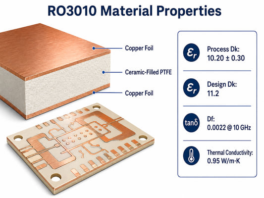
The official Rogers RO3010 datasheet should be the primary reference for material properties. The following values are typical rather than guaranteed finished-board measurements.
| Property | Typical RO3010 value | Practical relevance |
|---|---|---|
| Material composition | Ceramic-filled PTFE | Provides high-frequency performance and high Dk |
| Process Dk | 10.20 ± 0.30 | Used for laminate quality and material acceptance |
| Design Dk | 11.2 | Starting value for RF circuit modeling |
| Dissipation factor | 0.0022 at 10 GHz | Indicates dielectric loss |
| Thermal coefficient of Dk | −395 ppm/°C | Important for temperature-sensitive RF circuits |
| Thermal conductivity | 0.95 W/m·K | Helps estimate heat flow through the dielectric |
| X/Y/Z-axis CTE | 13/11/16 ppm/°C | Supports dimensional and plated-hole reliability |
| Water absorption | 0.05% | Limits moisture-related electrical change |
| Copper peel strength | 9.4 lb/in for 1 oz ED copper | Relevant to copper adhesion |
| Density | 2.8 g/cm³ | Higher than many lower-Dk PTFE laminates |
| Flammability rating | UL 94 V-0 | Relevant to product safety requirements |
| Lead-free compatibility | Yes | Supports lead-free assembly processes |
The high Dk and relatively low dissipation factor explain why RO3010 is attractive for compact microwave circuits. Its negative thermal coefficient of Dk should still be included in frequency-drift calculations when the product operates across a wide temperature range.
Which RO3010 Dk Value Should Engineers Use?
RO3010 has both a process Dk and a design Dk because they serve different purposes.
The process Dk of 10.20 ± 0.30 is measured using a defined material test method. It is mainly used to confirm that the laminate meets its manufacturing specification. It should not automatically be entered into every microstrip, stripline, or grounded coplanar waveguide model.
The design Dk of 11.2 is derived to represent practical circuit behavior more closely and is generally the better starting point for RF modeling. Even so, it is not a substitute for a production stackup. Effective permittivity also changes with:
- Dielectric thickness
- Copper thickness and conductor profile
- Transmission-line structure
- Solder mask coverage
- Frequency
- Etched trace shape
- Local resin or bonding-layer geometry
For a controlled-impedance PCB, the designer and manufacturer should use the same Dk assumption, copper model, and finished dielectric thickness. Prototype correlation or a representative impedance coupon is advisable when the design has narrow tolerances or phase-sensitive structures.
When Is RO3010 the Right Material for an RF PCB?
RO3010 is a strong candidate when circuit miniaturization is a primary requirement. Its high Dk can reduce the dimensions of patch antennas, filters, resonators, couplers, and impedance-matching networks without relying on an extremely thin dielectric.
It is particularly useful when a design needs:
- Compact RF structures
- Low dielectric loss at microwave frequencies
- A CTE relatively close to copper
- Stable mechanical properties for multilayer construction
- A ceramic-filled PTFE material for broadband components
RO3010 may be unnecessary for low-frequency control boards, power distribution boards, ordinary digital electronics, or RF circuits that already meet size and loss requirements on a lower-cost material. A lower-Dk laminate may also provide wider conductors, less concentrated electric fields, or greater antenna bandwidth.
Temperature deserves separate attention. RO3010 has a typical TCDk of −395 ppm/°C. A filter, oscillator, or narrowband antenna exposed to a large temperature range should be modeled for frequency shift before the material is approved.
Which RO3010 Thickness and Copper Options Fit the Stackup?
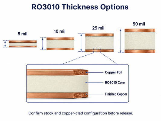
Rogers RO3010 thickness affects trace width, impedance, coupling, radiation, mechanical stiffness, and the physical size of resonant structures. Common published RO3010 thicknesses include the following options.
| Nominal thickness | Metric equivalent | Typical design consideration |
|---|---|---|
| 5 mil | 0.127 mm | Compact structures, very narrow lines, demanding handling |
| 10 mil | 0.254 mm | Thin RF layers with moderate mechanical support |
| 25 mil | 0.635 mm | Wider conductors and greater rigidity |
| 50 mil | 1.270 mm | Mechanically stronger boards and thicker RF substrates |
A thickness should not be selected from availability alone. The engineer should first model the transmission-line geometry, conductor loss, field confinement, and fabrication tolerance. A 5 mil core may reduce overall thickness but can introduce fragile handling and very small trace features. A thicker core may improve rigidity while producing wider conductors or larger circuit elements.
PCB quotations commonly involve 0.5 oz, 1 oz, or 2 oz finished copper. Availability depends on the selected laminate thickness and copper-clad configuration. Base foil and finished copper are not the same value because plating increases copper thickness in plated areas. Both values should be stated in the stackup.
How Does Rogers RO3010 Compare with RO3210?
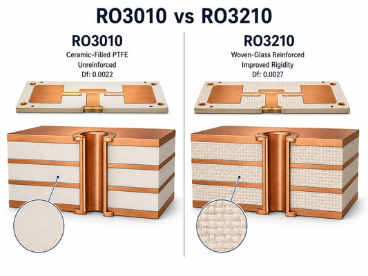
RO3010 and RO3210 have a similar nominal process Dk, but their reinforcement and mechanical behavior are different. The choice is mainly between the homogeneity of an unreinforced ceramic-filled PTFE material and the added rigidity of woven-glass reinforcement.
| Comparison point | RO3010 | RO3210 |
|---|---|---|
| Material structure | Ceramic-filled PTFE | Ceramic-filled laminate with woven fiberglass |
| Process Dk | 10.20 ± 0.30 | 10.20 ± 0.50 |
| Dissipation factor | 0.0022 at 10 GHz | 0.0027 at 10 GHz |
| Mechanical rigidity | Softer and more flexible during handling | More rigid and easier to handle |
| Registration control | Requires careful support, especially on thin cores | Improved by woven-glass reinforcement |
| Multilayer use | Suitable with controlled handling and lamination | Well suited to complex multilayer and hybrid builds |
| Fine-line processing | Depends heavily on core support and etch control | Smooth surface supports fine-line etching |
| Routed edge quality | Generally cleaner without glass reinforcement | Glass reinforcement can affect edge quality |
| Typical selection reason | Lower loss and homogeneous dielectric structure | Improved rigidity and production handling |
RO3010 is often preferred when its lower Df and unreinforced structure support the electrical design. RO3210 becomes attractive when handling, registration, or multilayer process stability carries more weight. The final choice should be confirmed through simulation and fabrication review rather than Dk alone.
What Makes Rogers RO3010 PCB Manufacturing Difficult?
RO3010 can be fabricated into double-sided and multilayer boards, but it should not be processed as ordinary FR4. The Rogers RO3000 and RO3200 fabrication guidelines identify several areas that require special control.
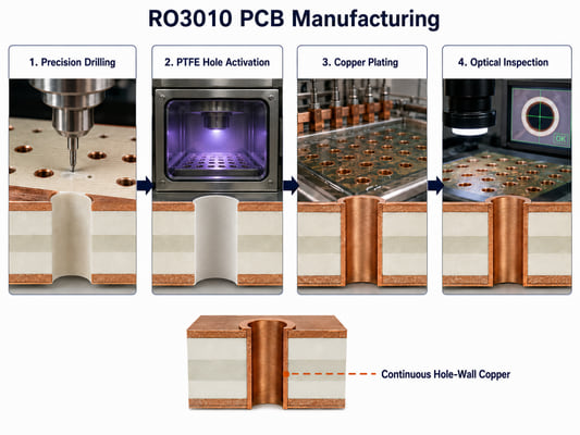
- Material handling: PTFE-based cores are softer than standard rigid laminates. Thin panels can crease, distort, or collect surface damage if carried by one edge or processed without support.
- Drilling: Sharp carbide tools, suitable entry and backup materials, controlled hit counts, and inspected hole quality are needed. Tool life should be based on actual hole cross-sections.
- Hole-wall activation: Drilled PTFE surfaces must be treated before electroless copper or direct metallization. Skipping sodium or plasma activation can cause weak copper adhesion or plated voids.
- Layer registration: Thin cores require appropriate tooling, copper balance, and panel support. Retaining copper around tooling areas can improve dimensional control.
- Multilayer bonding: The bonding material and press cycle must match the electrical target, flow requirement, and construction. Rogers bondply, thermoset prepreg, and thermoplastic film do not produce identical dielectric or processing results.
Surface finish also needs attention. Rogers notes that ENIG should be used on high-Dk RO3010 only when required because background plating can occur on exposed substrate surfaces.
How Should Controlled Impedance Be Managed on RO3010?
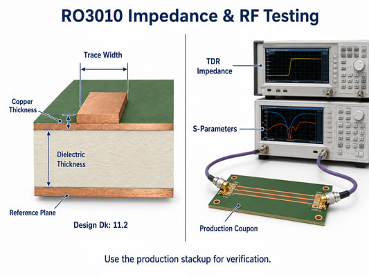
Controlled impedance begins before CAM engineering. The design package should define the material grade, nominal dielectric thickness, copper weight, transmission-line type, reference plane, target impedance, and acceptable tolerance.
RO3010’s high Dk can produce narrow 50-ohm conductors, particularly on thin dielectric layers. A small etch deviation may therefore create a meaningful impedance shift. Reliable control requires the fabricator to account for finished trace width, trapezoidal conductor shape, plating buildup, copper roughness, and the actual pressed dielectric thickness.
The most practical workflow is:
- Release a proposed stackup with target impedances.
- Let the fabricator calculate manufacturable trace geometries.
- Update the design before production files are frozen.
- Place a representative impedance coupon on the production panel.
- Test the coupon with TDR using the agreed test conditions.
- Record the result against the material lot and production batch.
For filters, phased structures, or matched RF paths, impedance alone may not be sufficient. Phase length and insertion-loss requirements should be specified separately.
How Should an RO3010 PCB Be Tested?
A standard bare-board electrical test checks continuity and isolation, but it does not prove microwave performance. Inspection and testing should match the actual design risk.
- AOI: Confirms trace geometry, clearances, opens, and shorts before solder mask.
- Microsection analysis: Evaluates hole-wall copper, plating continuity, registration, and dielectric structure.
- Bare-board electrical test: Verifies connectivity and isolation.
- TDR testing: Measures the impedance of controlled transmission lines through a representative coupon.
- Material verification: Confirms the Rogers grade, thickness, copper configuration, and lot documentation.
- S-parameter testing: Measures insertion loss, return loss, phase, or coupling when the customer supplies defined fixtures, calibration conditions, reference planes, and acceptance limits.
An RF test requirement should never be written simply as “test at high frequency.” The RFQ must define the frequency range, port configuration, connector or fixture, calibration method, reference plane, and pass/fail limit. Without these inputs, different test setups can produce results that are not directly comparable.
Which Applications Use Rogers RO3010 PCB?
RO3010 is most useful where a high dielectric constant creates a measurable size or integration benefit. Typical applications include:
- Compact microstrip and patch antennas
- GPS and wireless communication antenna boards
- RF filters, resonators, and couplers
- Power-amplifier matching networks
- Satellite communication modules
- Microwave sensors and measurement circuits
- Broadband communication components
- Selected radar and high-frequency RF modules
- Cable-system datalink circuits
- High-Dk multilayer or hybrid RF stackups
The application name alone is not enough to justify the material. For example, a large broadband antenna may benefit more from a lower-Dk substrate, while a compact narrowband antenna may make good use of RO3010. Frequency, bandwidth, board area, temperature range, conductor loss, and manufacturing tolerance should drive the decision.
What Determines Rogers RO3010 PCB Price?
There is no reliable fixed Rogers RO3010 price per piece for a custom PCB. A small two-layer board using stocked material and standard tolerances can have a very different cost structure from a multilayer hybrid board with tight impedance, small holes, and RF testing.
The main price factors are:
- RO3010 thickness and copper-clad availability
- Board dimensions and panel utilization
- Layer count and overall stackup
- Pure RO3010 or Rogers/FR4 hybrid construction
- Finished copper weight
- Minimum line width and spacing
- Hole diameter, aspect ratio, and via structure
- Impedance tolerance and coupon requirements
- Surface finish
- Microsection, TDR, or RF testing
- Prototype quantity and production forecast
- Standard or expedited lead time
Material waste can be a substantial cost driver. An irregular outline or unfavorable array may consume nearly the same panel area as a larger board. Allowing the manufacturer to review panelization before quotation can improve both cost and material utilization.
What Should You Verify with a Rogers RO3010 PCB Manufacturer?
A supplier should demonstrate more than general high-frequency PCB experience. The evaluation should focus on the processes that directly affect RO3010 performance and reliability.
Confirm whether the manufacturer can:
- Purchase traceable Rogers material in the required thickness
- Separate process Dk from design Dk during engineering review
- Handle and register thin PTFE cores
- Activate PTFE hole walls before metallization
- Select a suitable bonding system for multilayer or hybrid boards
- Compensate RF traces for the actual etching process
- Provide impedance calculations and production coupons
- Inspect plated holes through microsection analysis
- Supply material, test, and production traceability records
- Support prototypes without changing the approved production stackup
EBest Circuit uses the quotation and DFM stage to check the laminate grade, dielectric thickness, copper configuration, bonding system, impedance geometry, and test requirements. This review is particularly useful when a customer is moving from an RF simulation or early prototype to repeat production.
What Files Are Needed for a Rogers RO3010 PCB Quote?
A material name and board size are not enough for an accurate quotation. The PCB manufacturer should receive a package that defines both the mechanical build and the electrical intent.
Include the following information:
- Gerber or ODB++ production files
- NC drill and route files
- Fabrication drawing
- Proposed stackup
- Exact Rogers material grade
- Core and bonding-layer thicknesses
- Base and finished copper weights
- Overall finished board thickness
- Controlled-impedance targets and tolerances
- Operating frequency or frequency range
- Surface finish
- Solder mask requirements
- Quantity for prototype and expected production
- Electrical, TDR, microsection, or RF test requirements
- Applicable IPC class or customer specification
- Required delivery date
For an assembled RF board, also provide the BOM, component placement file, assembly drawing, stencil requirements, RF connectors, test procedure, and any components that require controlled handling. Complete inputs reduce quotation assumptions and make supplier comparisons more meaningful.
FAQs About Rogers RO3010 PCB
Is Rogers 3010 the same as RO3010?
Yes. “Rogers 3010” is commonly used as shorthand, while RO3010 is the correct Rogers product designation.
Is RO3010 a PTFE material?
Yes. RO3010 is a ceramic-filled PTFE composite developed for commercial microwave and RF circuits.
What is the dielectric constant of RO3010?
Its process Dk is 10.20 ± 0.30, while its published design Dk is 11.2. The design value is normally the better starting point for circuit modeling.
What RO3010 thicknesses are commonly available?
Common published thicknesses include 5, 10, 25, and 50 mil, corresponding to approximately 0.127, 0.254, 0.635, and 1.270 mm. Current stock and copper-clad combinations should be confirmed before the design is released.
Can RO3010 be used in a multilayer PCB?
Yes. Multilayer construction is possible, but the bonding material, press cycle, layer registration, hole preparation, and final dielectric thickness must be controlled.
Can RO3010 be combined with FR4?
Yes, Rogers/FR4 hybrid stackups are possible. The design needs an engineering review covering bonding compatibility, CTE differences, drilling, registration, dielectric properties, and lamination conditions.
Is RO3010 suitable for 77 GHz radar?
It may be considered for very-high-frequency circuits, but suitability at 77 GHz cannot be determined from a frequency rating alone. Copper roughness, line geometry, temperature drift, fabrication tolerance, loss, and prototype RF results should be evaluated; another Rogers material may be more appropriate for a specific radar design.
How can I get an accurate RO3010 PCB price?
Provide the Gerber files, stackup, material thickness, copper weight, impedance requirements, surface finish, test plan, quantity, and delivery target. These details allow the manufacturer to calculate material use and process cost rather than relying on a generic unit price.
Conclusion
Rogers RO3010 PCB material is best suited to RF and microwave designs that benefit from high Dk, compact circuit structures, low dielectric loss, and controlled mechanical properties. Its advantages are most valuable when the stackup, temperature behavior, trace geometry, PTFE processing, and verification plan are considered together. For general electronics or designs without space constraints, a less specialized laminate may offer a simpler and more economical route.
To review an RO3010 prototype or production requirement, send your Gerber files, stackup, dielectric thickness, copper weight, target impedance, operating frequency, quantity, and test requirements to sales@bestpcbs.com. EBest Circuit can evaluate material availability, manufacturability, testing scope, and quotation details before fabrication.