Power electronics interconnects affect how much heat a power assembly generates, how it behaves during fast switching, and how its connections age. A cool busbar can still have an overheated terminal. A thick copper path can still produce a switching-voltage spike. Understanding the connection itself helps explain why these problems occur.
EBest Circuit (Best Technology) supports PCB fabrication, component sourcing, SMT and through-hole assembly, inspection, and agreed testing. Coordinating fabrication and assembly helps address board-level details such as solderability and terminal-to-hole fit before they become assembly problems. For PCB and PCBA support around your approved power circuit, contact sales@bestpcbs.com.
What Are Power Electronics Interconnects?
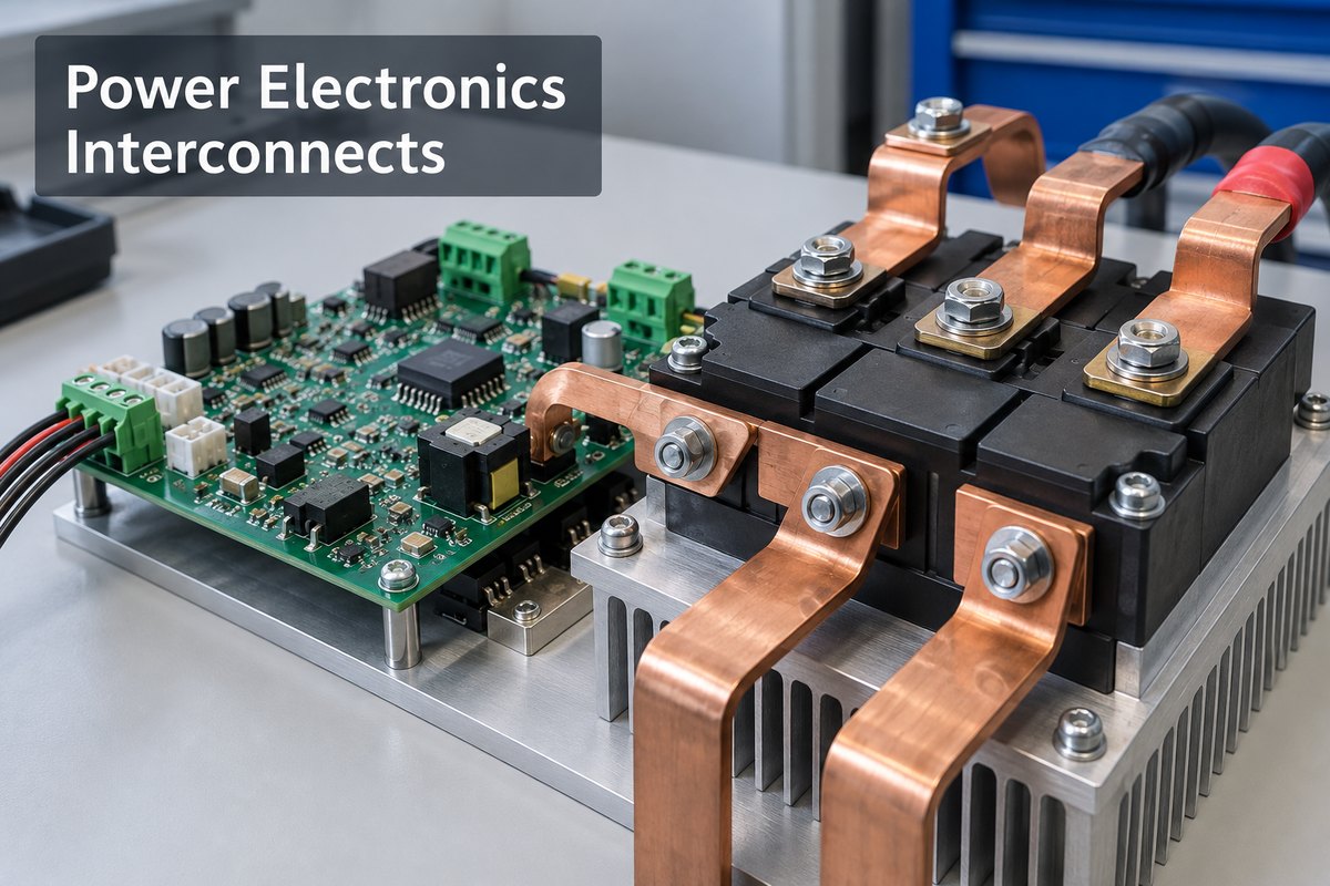
Power electronics interconnects are the conductive connections that carry current through a power assembly—from the semiconductor die to the PCB, power module terminals, and external conductors.
They exist at three levels within the assembly.
- Inside the package — Bond wires, ribbons, clips, and conductive die-attach layers connect the semiconductor to its package conductors.
- On the PCB — Solder joints, copper tracks, planes, and plated holes carry current between components.
- Between assemblies — Module terminals, connectors, cables, and busbars link the board to the wider power system.
A removable connector is therefore only one type of interconnect. Every joint along the current path matters; adding copper elsewhere cannot eliminate a restrictive connection.
How Do Wire Bonds, Copper Clips, and Die Attach Differ?
Wire bonds and copper clips commonly connect the top of the die; die attach joins its underside to a support. They occupy different positions, so die attach is not a direct replacement for a wire or clip.
| Structure | Connection form | Main performance considerations |
|---|---|---|
| Wire bonds | Wires from die pads to package conductors | Wire resistance, inductance, and current sharing |
| Copper clips | Broad copper connections above the die | Connection resistance and inductance |
| Die attach | Bonded layer beneath the die | Heat transfer; current flow when conductive |
A short, broad copper clip can reduce resistance and inductance compared with a suitable wire-bonded alternative. The benefit depends on the complete package geometry; some packages use both clips and wires for different terminals.
Die attach has a separate job. Soldered or sintered layers provide a heat path from the die into its support and may also carry current. A good top-side connection cannot compensate for poor heat transfer beneath the die.
How Do PCBs Connect to Power Modules and Busbars?
PCBs connect to power modules and busbars through soldered terminals, press-fit pins, bolted terminals, or mating connectors. Each interface carries current and transfers mechanical forces differently.
| Interface | Connection method | Key assembly consideration |
|---|---|---|
| Soldered terminal | Solder joins terminal and PCB | Adequate heat at the joint |
| Press-fit terminal | Pin presses against a plated hole | Matched pin, hole, and plating |
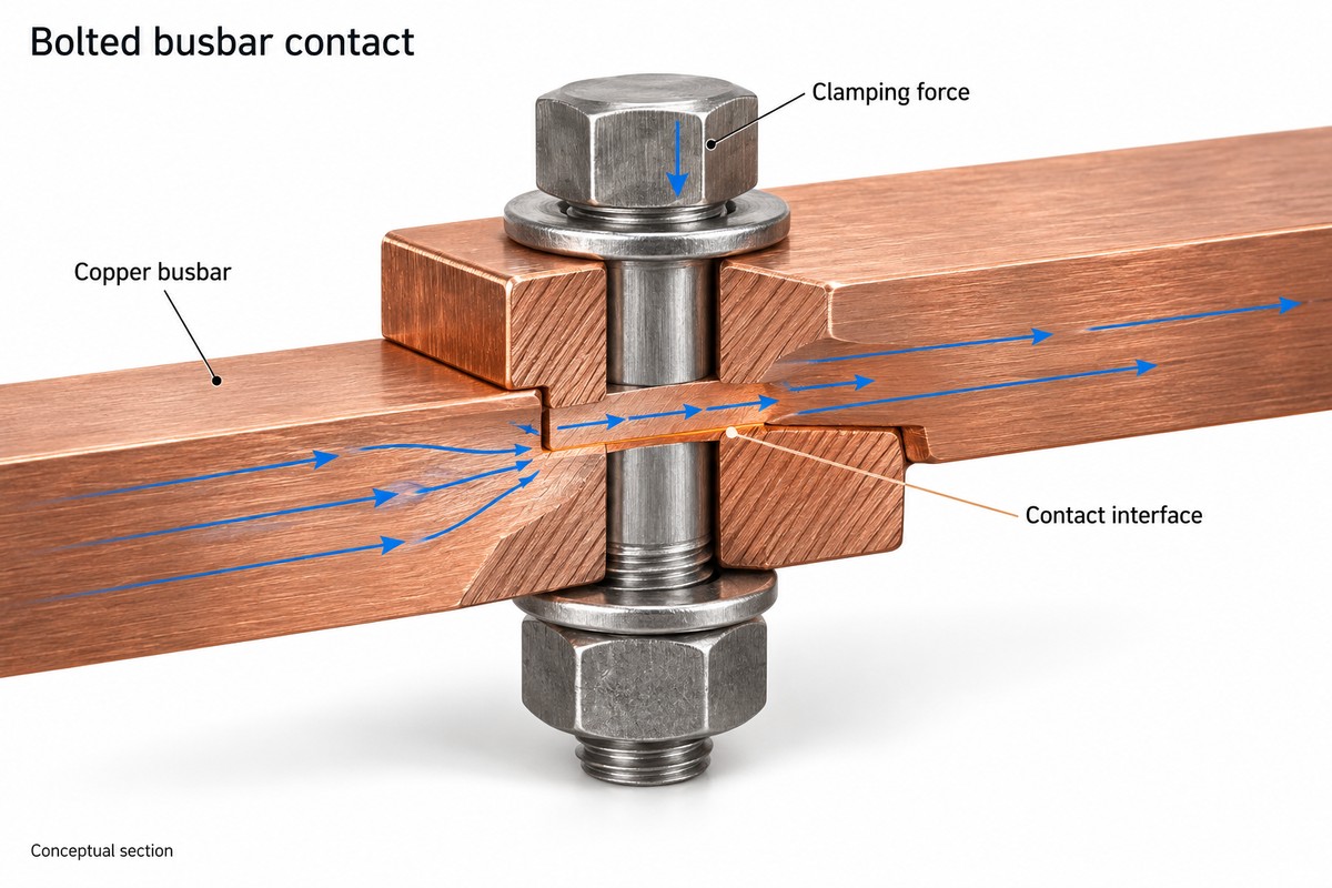
| Bolted terminal | Fastener clamps conductive surfaces | Contact pressure and mechanical support |
| Mating connector | Designed contacts plug together | Mating limits and contact rating |
Large copper terminals can draw heat away during soldering, making joint formation harder. Press-fit connections avoid that soldering step, but require the specified hole construction, insertion tooling, and board support.
Press-fit does not automatically mean pluggable. It describes the terminal’s connection to the PCB. A separate mating interface provides repeated plugging and unplugging.
Busbars often carry bulk current between modules and DC-link capacitors, while PCBs carry control, sensing, and other circuit connections. For dimensional options, see standard copper busbar sizes. Width and thickness help describe a busbar, but do not establish its installed current rating by themselves.
Why Do Power Interconnects Overheat?
A connection can overheat even when the larger conductor beside it stays cool. The hot spot may be a narrow track, a terminal contact, or a joint where resistance concentrates heat.
Three conditions explain much of this behavior.
- High current magnifies small resistance. Resistive loss follows P = I²R. Doubling current produces four times the heat at the same resistance.
- A small connection can restrict a large current path. A wide busbar does not remove resistance at its terminal. Adding copper away from that joint may leave the hot spot unresolved.
- Heat cannot escape fast enough. Limited airflow, a crowded enclosure, and nearby hot components can raise the connection’s temperature even without a change in current.
A small resistance can produce meaningful heat. For illustration, a 0.5 mΩ connection dissipates 5 W at 100 A and 20 W at 200 A. These are calculated losses at constant resistance, not temperature rises or current ratings.
Actual operating temperature depends on both heat generation and heat removal. Copper resistance also rises with temperature, so room-temperature resistance alone may understate operating losses.
How Does Parasitic Inductance Affect Fast Switching?
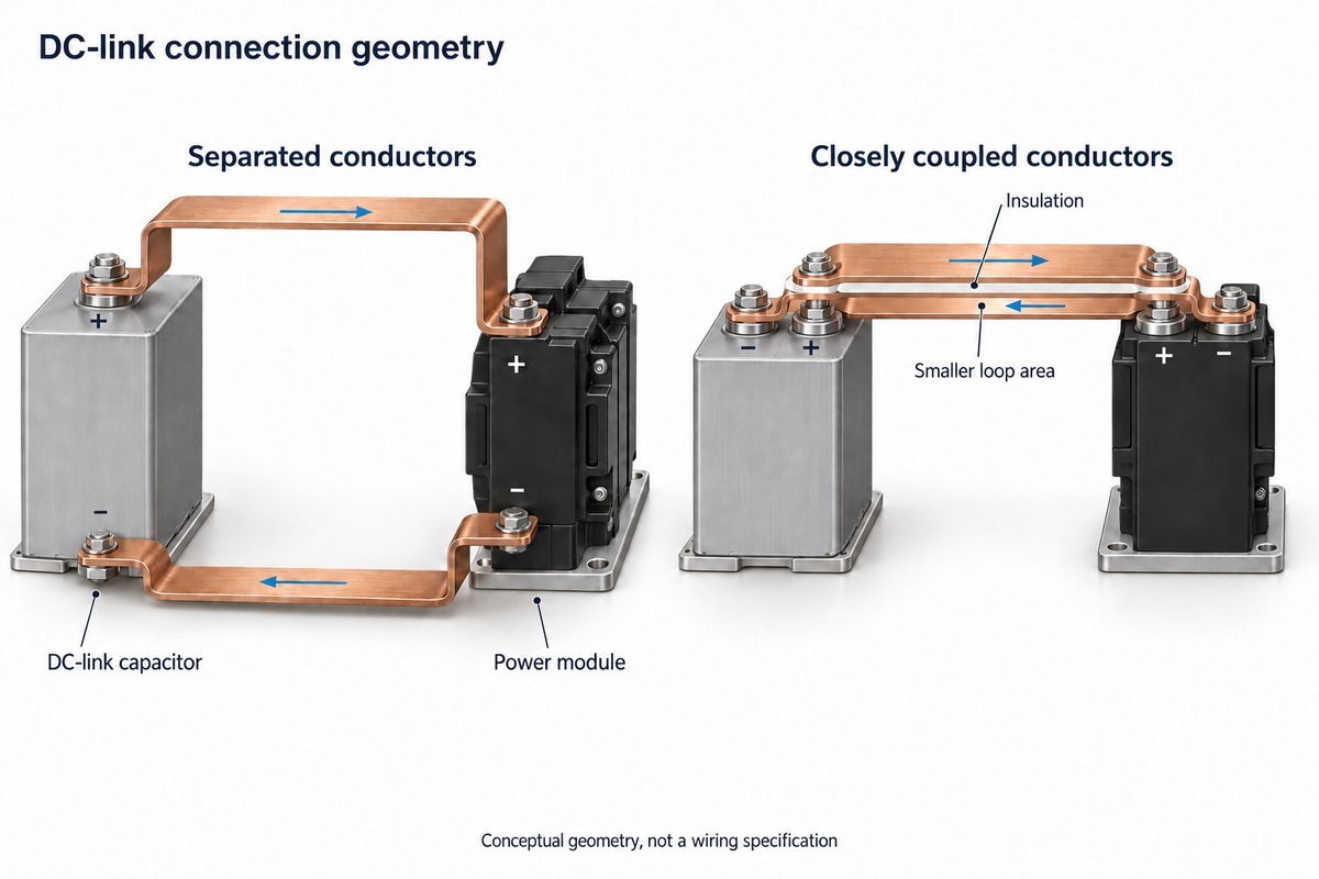
A low-resistance connection can still create a voltage spike during fast switching. Its inductance generates an additional voltage as current changes, following ΔV = L × di/dt.
For illustration, 20 nH at 500 A/µs contributes 10 V. This is the inductive contribution, not a prediction of the complete switching waveform.
The important geometry is the complete current loop, including its return path. A thick conductor with a distant return path can still form a large loop. Two layout features help explain the difference.
- Nearby outgoing and return paths reduce loop inductance. Conductor thickness alone does not provide the same effect.
- A nearby decoupling capacitor can shorten the switching-current loop. Long connections between the capacitor and switching devices add to that loop.
Package terminals and PCB connections contribute as well. Together with circuit capacitance, inductance can produce overshoot and ringing. This is why adding copper thickness may reduce resistive loss without resolving a switching-voltage problem.
What Causes Power Interconnects to Fail Over Time?
An initially sound connection can weaken through repeated heating and cooling. Joined materials expand by different amounts, placing cyclic strain on their interfaces.
The damage appears differently depending on the connection.
- Wire bonds can develop heel cracks or lift at the bond interface. Repeated strain damages the wire or its attachment point.
- Solder joints can develop fatigue cracks. Cyclic deformation progressively damages the connection.
- Die-attach layers can deteriorate. Damage beneath the die can impair heat transfer and raise operating temperature.
Pressure-based terminal connections have a different requirement: they must maintain suitable contact through service conditions. Mechanical support and the specified assembly process help preserve that interface.
Thermal cycling and power cycling stress an assembly differently. Thermal cycling changes its temperature through the surroundings. Power cycling heats the semiconductor through electrical operation, often concentrating temperature changes near the die. Passing one test does not automatically establish performance under the other.
A room-temperature resistance measurement describes the connection’s initial condition. Durability depends on how that construction responds to the temperature changes and mechanical stresses it will experience in service.
FAQs About Power Electronics Interconnects
Are power electronics interconnects just connectors?
No. They also include package connections, PCB copper paths, solder joints, busbar interfaces, and die-attach layers that carry current. Connectors are one part of that wider current path.
Can a busbar replace the PCB?
A busbar can carry part of the bulk-current path, but does not normally replace the PCB’s control, sensing, and component-interconnection functions. Many power assemblies use both.
Does press-fit mean the connection is pluggable?
No. Press-fit describes how a terminal engages a plated board hole. Repeated mating requires an interface designed for it. Removing or replacing a press-fit component must follow the applicable product instructions.
Does low resistance mean low inductance?
No. A connection can have low resistance and still form a large current loop. Resistance influences conduction loss; loop inductance influences the additional voltage produced during rapid current changes.
Does high current always mean high voltage?
No. Low-voltage circuits can carry high current and generate substantial resistive heat. Voltage suitability involves separate insulation and spacing requirements. Both must match the application.
For PCB fabrication and assembly supporting power electronics interconnects, EBest Circuit (Best Technology) can review manufacturability and coordinate sourcing, assembly, inspection, and agreed testing. Contact sales@bestpcbs.com to discuss the board-level connections in your power assembly.