LGA usually fits high-contact-count platforms; PGA favors simple ZIF handling. Neither interface is better for every motherboard. The correct choice depends on the supported processor, routing density, power distribution, retention load, handling controls, inspection access, and service strategy.
The LGA vs PGA decision extends beyond where the pins sit. The motherboard must also support the socket-to-PCB joints, retention hardware, high-speed escape routing, power and ground paths, assembly sequence, contamination control, and test coverage.
Which Is More Suitable for PCB Design and Assembly: LGA or PGA?
Use LGA for dense platforms and PGA when the selected platform requires it. In practice, the processor vendor fixes the interface before motherboard design begins. The engineering decision is whether the PCB technology, assembly process, retention hardware, and service plan can support that socket.
| Decision dimension | LGA | PGA |
| Package interface | Flat lands on the processor mate with spring contacts in the socket | Pins on the processor enter contacts in the socket |
| Contact-density potential | Well suited to high-position-count processor platforms | Useful across many established socketed platforms |
| Retention | Usually depends on a load plate, frame, backplate, and specified compression | Commonly uses a ZIF lever to lock processor pins into socket contacts |
| Handling vulnerability | Exposed socket contacts can be damaged or contaminated | Exposed processor pins can bend during handling or removal |
| Field repair | A damaged socket contact can require specialist socket replacement or board replacement | A slightly bent processor pin may sometimes be recoverable by a qualified technician |
| PCB and assembly demand | Requires tight control of board flatness, socket soldering, retention load, and dense routing | Requires controlled socket soldering, pin-safe handling, ZIF actuation, and compatible routing |
Select the processor family first, then obtain the approved socket, retention hardware, and platform files. Before layout, confirm that the fabricator and assembler can meet the specified land pattern, board thickness, flatness, reflow, inspection, and handling limits. Missing inputs make either choice unsafe to release.
What Are LGA and PGA CPU Sockets, and How Do They Connect to a Motherboard?
Both designs connect a removable CPU through a board-mounted socket. During normal use, the CPU is not soldered to the motherboard. The socket is soldered to the PCB and can be replaced only through a qualified rework process.
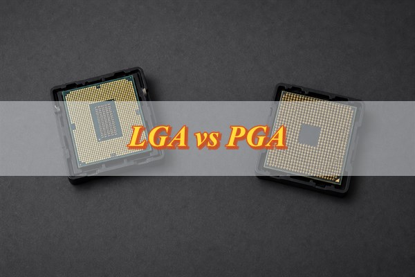
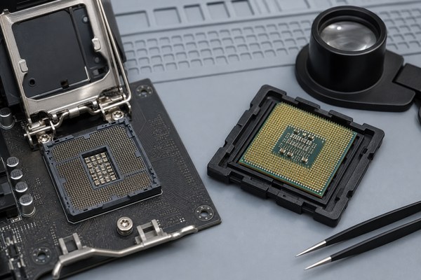
In a land grid array interface, the processor underside has flat metal lands. Fine spring contacts in the LGA socket deflect when the load mechanism closes and press against those lands. Many modern LGA sockets use solder-ball surface-mount terminations beneath the housing. The socket frame, load plate, and backplate align the package, apply the specified contact load, and limit PCB bending.
In a pin grid array interface, a regular array of pins extends from the processor package. With a common ZIF socket, the processor enters aligned openings with little force. A lever or actuator then engages the socket contacts. The socket may still use surface-mount terminations to connect to the board. Some specialized PGA sockets use other attachment styles, so the selected component drawing remains authoritative.
AMD specifies Socket AM5 as a 1718-position LGA platform and AM4 as a 1331-opening PGA interface. Intel issues separate installation instructions for LGA1700 and LGA1851. Each platform needs its own footprint, retention hardware, and cooler limits.
- CPU-to-socket interface: compression against lands for LGA; captured package pins for PGA.
- Socket-to-PCB interface: commonly a soldered array beneath the socket, not the removable CPU contact field.
- Mechanical load path: processor, socket contacts, load or lock mechanism, PCB, backplate, and cooler hardware interact as one system.
- Electrical path: processor contact, socket contact, socket termination, PCB pad, via structure, and routed plane or trace all contribute resistance and inductance.
A continuity fault may occur at the package contact, socket contact, actuator, hidden socket solder joint, deformed PCB, or routed network. Inspect the full connection path instead of replacing the processor first.
What Are the Main LGA vs PGA Differences in Contact Structure and Density?
LGA puts spring contacts in the socket; PGA puts pins on the CPU. This changes handling risk, inspection method, retention, achievable contact geometry, and which component is damaged by a handling error.
| Contact characteristic | LGA socket and processor | PGA socket and processor |
| Processor underside | Flat plated lands and, depending on package, passive components in defined keepout areas | Regular pin array with orientation keys and an exclusion pattern |
| Socket mating element | Compliant spring contacts that wipe or press against package lands | Receptacle contacts that close around processor pins |
| Actuation objective | Apply specified, distributed compression without sliding the package across contacts | Accept pins at low force, then engage contacts through the ZIF actuator |
| Typical visible damage | Misaligned, flattened, contaminated, or missing socket contacts | Bent, twisted, contaminated, or missing processor pins |
| Density constraint | Contact geometry, pitch, force, routing escape, solder-joint pitch, and mechanical envelope | Pin pitch, pin stiffness, socket openings, ZIF mechanism, routing escape, and mechanical envelope |
| Repair boundary | Individual contact work is delicate and often outside approved board-level repair practice | Minor pin alignment may be possible, but fractured or fatigued pins are not a simple cosmetic defect |
Position count alone does not prove better electrical performance. High-position-count LGA platforms are common, but PGA platforms have also supported high-speed memory and PCIe connections. The processor pin map, power-to-signal ratio, reference-plane design, socket model, and channel budget determine usable performance.
Density also increases PCB consequences. More contacts can mean finer escape routing, more signal-reference transitions, greater demand for via-in-pad or fine-drill strategies, and less room for voltage-regulator placement near the socket. Those trade-offs must be evaluated using the processor design guide and the exact socket footprint rather than a generic LGA vs PGA diagram.
How Do LGA and PGA Affect Signal Integrity, Power Delivery, and Thermal Cycling?
LGA and PGA both affect the electrical path between the CPU and motherboard. Their contacts add resistance and inductance, which can influence signal quality and power delivery.
The exact effect depends on the selected processor, socket, and PCB layout. Check them together when reviewing high-speed signals, power distribution, and reliability during temperature changes.
For signal integrity, the socket is part of the transmission path. Contact length, return contacts, breakout vias, antipads, layer transitions, and plane discontinuities affect impedance and crosstalk. A short route is not automatically a good route if it crosses a reference-plane split or uses an uncontrolled via field.
Memory, PCIe, and other fast interfaces should follow the processor vendor’s topology, length-matching, reference, and loss limits. When models are available, simulation should include the package, socket, PCB, connector, and device at the intended data rate.
For power delivery, a processor uses many parallel power and ground contacts to reduce effective resistance and inductance. The PCB must connect those contacts into a low-impedance power-distribution network with suitable planes, via arrays, decoupling placement, copper distribution, and voltage-regulator layout. Removing “redundant-looking” ground or power vias to simplify routing can concentrate current and weaken the return path. Thermal-via and copper decisions must also respect socket keepouts and backplate clearance.
Thermal cycling changes dimensions across the processor package, socket housing, solder joints, PCB, retention frame, and cooler. Repeated expansion and contraction can alter contact force or stress socket-to-board joints, particularly when the board is bowed or the cooler load is uneven. LGA compression systems make the load path especially visible, but PGA systems are not exempt: socket solder joints, package pins, and the PCB still experience cyclic strain.
- Signal review: confirm reference continuity, breakout-via geometry, differential-pair rules, crosstalk spacing, and channel-model assumptions.
- Power review: confirm every required power and ground connection, plane transitions, via current paths, decoupling loops, and regulator-to-socket distribution.
- Mechanical review: evaluate board thickness, local stiffness, backplate contact, cooler torque sequence, warpage, and chassis support.
- Reliability review: qualify the complete assembly through the temperature, power-cycling, vibration, and handling conditions that represent the application.
How Do LGA and PGA Compare in Mechanical Durability and Repairability?
LGA shifts handling risk to the motherboard socket, while PGA shifts it to the processor pins. Compare the damaged part, approved repair method, inspection access, and replacement cost before choosing a service strategy.
| Mechanical factor | LGA | PGA |
| Most vulnerable part | Fine spring contacts inside the motherboard socket | Exposed pins on the processor package |
| Common handling damage | Contacts can be displaced by fingers, tools, a dropped cover, or a CPU inserted at an angle | Pins can bend when the CPU is placed pin-side down, removed at an angle, or pulled with the cooler |
| Required protection | Keep the socket cover installed until CPU insertion and whenever the socket is empty | Keep the processor in a rigid pin-protection carrier whenever it is outside the socket |
| Inspection method | Inspect contact rows under magnification for height, direction, contamination, and missing contacts | Inspect the pin array from two directions for straightness, spacing, contamination, and missing pins |
| Permitted repair boundary | Adjust a contact only when the socket supplier or repair authority provides an approved method | Realign a slightly bent pin only with controlled support and magnification; avoid repeated bending |
| Replacement trigger | Replace the socket or motherboard when contacts are missing, folded, plated surfaces are damaged, or contact force cannot be verified | Replace the processor when pins are missing, cracked at the package, repeatedly bent, or deformed across a wide area |
| Board-level mechanical risk | Incorrect load plate, backplate, or cooler force can bow the PCB and change contact pressure | Incorrect cooler mounting or unsupported PCB areas can stress the socket joints and motherboard |
Before production release, define four controls:
- Handling: specify the socket cover, CPU carrier, ESD controls, and permitted contact surfaces.
- Installation: document processor orientation, vertical insertion, lever operation, cooler sequence, and approved load.
- Inspection: define magnification, visual acceptance criteria, and who can authorize repair.
- Service decision: compare processor replacement, socket rework, motherboard replacement, inspection time, and latent-failure risk.
How Should a Motherboard PCB Be Designed for an LGA or PGA Socket?
Lock the exact socket footprint and mechanical stack before routing. Confirm the socket part number and revision, processor pin map, board thickness, pad and mask dimensions, mounting holes, keepouts, backplate, and cooler load.
Next, confirm that the planned stackup and via technology can escape the contact array while preserving reference planes and power paths. If any input is missing, stop layout. A late footprint or retention change can force new routing, a different stackup, or a complete board revision.
- Freeze the processor, socket, and hardware set. Confirm the processor family, approved socket part number, retention mechanism, backplate, cooler envelope, board thickness range, mounting holes, keepouts, and compatibility list. Do not assume that similar contact counts share geometry or pin assignments.
- Import controlled CAD data. Build the footprint from the released product drawing or validated library. Verify pad coordinates, mask rules, paste requirements, orientation features, courtyard, socket-cap clearance, underside backplate area, and component-height restrictions. Perform an independent pin-one and net-map check.
- Plan stackup and escape routing. Allocate reference planes and routing layers before fanning out the array. Determine via type, drill capability, aspect ratio, antipad geometry, annular-ring margin, and whether blind, buried, or via-in-pad structures are justified. Keep reference transitions close to signal transitions where the platform guide requires them.
- Build the power-distribution network. Map power and ground contacts to planes and copper regions, preserve required parallel paths, place decoupling for short current loops, and check current density through neck-downs and via groups. Coordinate voltage-regulator placement with cooler, socket, and routing keepouts.
- Control mechanical stiffness and warpage. Model the retention and cooler load through the PCB and backplate. Check board thickness, copper balance, local cutouts, mounting support, large component placement, and chassis constraints. Avoid routing or placing fragile parts where the board is expected to flex.
- Run signal and power verification. Simulate critical channels with the available package and socket models. Review impedance, insertion loss, return loss, crosstalk, reference continuity, simultaneous switching, DC drop, and transient behavior against platform limits.
- Complete DFM and release evidence. Confirm the fabricator can produce the selected stackup and via structure, and that the assembler can print, place, reflow, inspect, and rework the socket. Release fabrication drawings, assembly drawings, approved component data, controlled profiles, inspection criteria, and test access as one consistent package.
Do not release the board until socket geometry, backplate clearance, and cooler load are verified. A late correction can force rerouting, expose copper, collide with backside components, or distort the contact field.
How Should LGA and PGA Socket Assemblies Be Installed, Inspected, and Tested?
Approve the socket soldering before installing the CPU. Verify paste printing, placement, reflow profile, housing position, and hidden solder joints against the selected socket requirements.
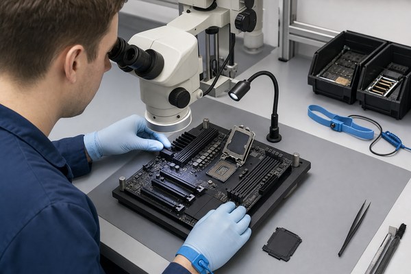
After soldering passes, inspect the LGA contacts or PGA pins, install the processor vertically, lock the mechanism, and mount the cooler using the specified sequence and load. Then test power rails, processor detection, memory channels, high-speed interfaces, and temperature under load. A successful boot alone does not prove that every contact is reliable.
- Verify incoming parts and storage. Check socket part number, revision, packaging condition, contact protection, moisture-handling requirements, processor carrier, retention hardware, and traceability. Quarantine parts with crushed trays, displaced caps, visible contamination, or contact damage.
- Prepare the PCB and printing process. Confirm board flatness, pad cleanliness, stencil revision, support tooling, paste condition, and registration. The stencil aperture strategy must match the socket supplier’s application requirements; it should not be generalized from another large array component.
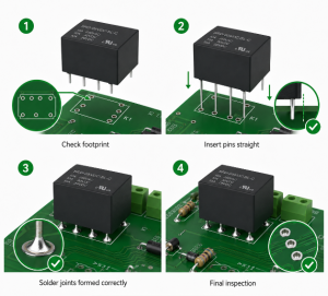
- Place the socket with proper support. Use the approved pickup feature or cap, maintain orientation, avoid housing distortion, and support the PCB so placement force does not bow the array. Inspect for gross offset before reflow.
- Reflow with a qualified profile. Measure the assembly rather than relying only on oven setpoints. Confirm heating rate, soak, peak, time above liquidus, cooling, and temperature variation remain within the solder-paste, PCB, and socket limits. Protect plastic housings and large thermal masses from an unsuitable profile.
- Inspect socket-to-board attachment. Use visual inspection for housing position and accessible joints, then apply X-ray or another validated method where terminations are hidden. Evaluate alignment, opens, bridges, solder distribution, and abnormal voiding against the approved criteria for that socket.
- Inspect the CPU contact interface. Keep the protective cap in place until the defined installation point. For LGA, inspect contact rows under magnification and do not touch them. For PGA, inspect pin straightness and cleanliness while the processor remains supported in its carrier.
- Install and actuate the processor. Remove power, apply ESD controls, align keys or pin-one indicators, and lower the processor vertically. Do not slide an LGA package across contacts or force a PGA package into a closed or misaligned ZIF socket. Close the load plate or ZIF lever using the specified sequence.
- Install the thermal solution. Apply the specified interface material and tighten the cooler in the documented sequence and load range. Confirm the backplate and nearby components remain seated and the board is not visibly distorted.
- Test before release. Perform power-off resistance checks where appropriate, controlled first power-up, rail and clock checks, firmware identification, memory training, interface tests, thermal monitoring, and application-specific functional or stress testing. A passed boot screen alone does not prove every socket contact or solder joint is reliable.
What Failure Modes Affect LGA Contacts and PGA Socket Pins?
LGA and PGA fail at different exposed contacts. LGA faults often involve displaced or contaminated socket springs. PGA faults often involve bent CPU pins or incomplete ZIF engagement. Both can also fail at hidden socket-to-PCB joints or through PCB power, routing, and mechanical defects.
| Observed symptom | Possible LGA cause | Possible PGA cause | Useful verification |
| No boot or processor not detected | Mis-seated package, damaged contact, retention fault, open solder joint, or power issue | Bent or missing pin, open ZIF mechanism, incomplete seating, open solder joint, or power issue | Visual inspection, rail checks, reset and clock checks, socket-map continuity |
| Missing memory channel | Contact displacement, contamination, board bow, or routing defect on memory nets | Bent pin, incomplete pin engagement, socket fault, or routing defect | Pin-map correlation, magnified inspection, known-good memory, continuity and channel test |
| Intermittent failure under load | Marginal contact force, thermal movement, cooler-load distortion, or solder fatigue | Marginal pin contact, socket wear, contamination, or solder fatigue | Controlled thermal/power cycling, mechanical review, resistance trending |
| Local overheating or voltage droop | High-resistance contact, inadequate parallel power path, or PDN layout problem | Damaged power pin, poor receptacle engagement, or PDN layout problem | Voltage-drop mapping, thermal inspection, current-path and via review |
| Failure after service | Contact touched, package slid, protective cap dropped, or cooler tightened unevenly | Pins bent during removal, CPU forced, lever not locked, or cooler pulled processor | Before/after photographs, socket inspection, seating and torque review |
Contamination deserves special attention. Skin oils, fibers, thermal compound, cleaning residue, and debris can change contact resistance or prevent full seating. Aggressive cleaning can create more damage than the original contamination. Use only methods approved for the socket materials and contact plating, with controls for residue, static charge, drying, and mechanical force.
Failure analysis should correlate the failing function with the processor pin map before disturbing the assembly. If a memory channel, PCIe lane group, or power domain fails consistently, that mapping can narrow the inspection region. Preserve photographs, X-ray images, electrical measurements, cooler installation details, and thermal history. Replacing the CPU immediately may restore operation but erase evidence of the actual root cause.
What Selection and Assembly Mistakes Increase LGA or PGA Reliability Risks?
Generic footprints and uncontrolled handling create the highest risk. Approve the platform files, mechanical stack, socket soldering process, contact protection, and functional test plan before production release.
- Choosing by reputation instead of platform fit: “LGA is newer” or “PGA is easier to repair” does not replace compatibility, I/O, power, lifecycle, and service analysis.
- Using a generic footprint: small errors in pad coordinates, mask openings, keepouts, or orientation can affect hundreds of connections at once.
- Ignoring socket-to-PCB joints: visible CPU contacts may look perfect while hidden solder joints contain opens, bridges, or alignment faults.
- Reducing ground or power connections for routing convenience: this can increase return-path discontinuity, DC drop, local heating, and transient noise.
- Leaving mechanical design until layout completion: backplates, cooler fasteners, board support, and load zones can collide with vias, traces, or backside components.
- Handling without protective carriers: an uncovered LGA socket or unsupported PGA processor can be damaged during a single uncontrolled movement.
- Forcing installation: a correctly oriented PGA processor should enter an open ZIF socket without force, and an LGA processor should lower straight down without sliding.
- Accepting boot as the only test: partial contact failures can disable one channel, appear only when hot, or emerge under mechanical or electrical load.
- Attempting undocumented contact repair: visually improved pins or contacts may still have inadequate force, plating damage, fatigue, or hidden fractures.
- Changing socket, cooler, PCB stackup, or supplier without requalification: each change can alter soldering, warpage, contact load, or channel behavior.
The release checklist should identify the approved CPU and socket revisions, controlled drawings, PCB stackup, reflow profile, inspection method, retention hardware, cooler sequence, first-power procedure, functional coverage, and rework authority. Use the same controlled revision for prototypes and production.
FAQs About LGA vs PGA
Q1: Is LGA always better than PGA for a high-performance CPU?
A1: No; platform implementation matters more than the package acronym. LGA supports high contact counts and controlled compression, but performance still depends on the processor, socket model, power allocation, PCB channels, retention hardware, and cooling. A qualified PGA platform can outperform a poorly implemented LGA motherboard.
Q2: Is a PGA socket soldered through holes in the motherboard?
A2: Not necessarily; many processor PGA sockets use surface-mount attachment. The processor pins enter the removable ZIF interface, but the socket’s own terminations connect permanently to the PCB. Some specialized PGA sockets use through-hole attachment, especially in test or other specific applications. Confirm the termination style from the exact socket drawing instead of inferring it from the processor pins.
Q3: Can an LGA socket contact be safely straightened?
A3: Only within an approved repair process and by a qualified technician. LGA contacts are small compliant springs whose position, shape, plating, and normal force all matter. A contact that appears straight may still be fatigued or misaligned. Uncontrolled manipulation can damage adjacent contacts. When acceptance limits or repair authorization are unavailable, socket or board replacement is safer than an improvised adjustment.
Q4: Can bent PGA processor pins be repaired?
A4: Slight deformation may be recoverable, but every bend carries fatigue risk. The processor must be supported, inspected under magnification, and corrected with a controlled method that avoids twisting or repeated cycling. Missing pins, cracked package interfaces, severely folded areas, or pins that no longer remain aligned usually justify replacement. Electrical and functional testing is still required after any accepted repair.
Q5: Why can a motherboard boot even when a socket contact is defective?
A5: A basic boot does not exercise every interface or load condition. A marginal connection may affect one memory channel, a group of PCIe lanes, or a power return without stopping startup. Temperature and board flex can also hide an intermittent fault during a short check. Test coverage should exercise interfaces and power states, not stop at firmware detection.
Q6: Does the LGA vs PGA choice change PCB layer count?
A6: It can influence layer demand, but contact type alone does not set the layer count. The processor pin map, memory topology, PCIe generation, power planes, breakout density, via strategy, impedance rules, and board form factor drive the stackup. Dense LGA and PGA platforms can both require multilayer escape routing.
Q7: What is the safest way to store an unused LGA or PGA component?
A7: Protect the exposed contact system with its original ESD-safe packaging. Keep the LGA socket cap installed whenever no processor is present, and retain the processor’s protective carrier. Store a PGA processor in a rigid pin-protection tray rather than loose foam or a bag. Control moisture where specified, avoid contact with thermal compound, and label parts by verified platform and revision.
Q8: How does LGA vs BGA differ from LGA vs PGA?
A8: BGA is normally soldered directly to the PCB, while socketed LGA and PGA processors are removable. A BGA package uses solder balls between the component and board and generally requires reflow and specialized rework. LGA and PGA CPU sockets add a replaceable processor interface but also add socket contacts, retention hardware, and another soldered component beneath the CPU.
Q9: Should a used LGA or PGA socket be cleaned before CPU installation?
A9: Clean only when contamination is confirmed and an approved method is available. Compressed air, brushes, solvents, or wipes can bend contacts, spread debris, leave residue, or create static damage. Begin with magnified inspection under controlled lighting. If cleaning is necessary, follow the socket supplier’s material-compatible procedure and reinspect for particles, residue, and contact displacement.
Q10: What files should a PCB assembler receive for a socketed CPU motherboard?
A10: Release one controlled package covering fabrication, assembly, mechanics, and testing. Include Gerber or ODB++ data, drill files, stackup, impedance rules, approved BOM, socket drawings, centroid data, and assembly drawings. Add stencil requirements, profile limits, inspection criteria, cooler instructions, test access, firmware conditions, and acceptance requirements. Every file must use the same approved revision.
For a socketed processor project, send the approved CPU platform, socket part number, PCB stackup, fabrication data, BOM, assembly drawings, mechanical hardware, and test requirements. For PCB or PCBA engineering support from prototype through volume production, contact EBest Circuit for a technical review and quotation at sales@bestpcbs.com.