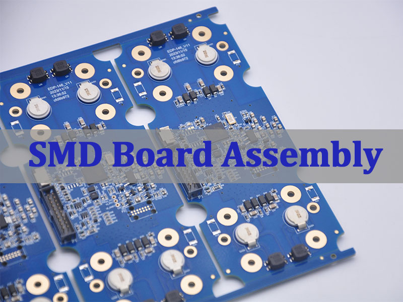
PCB button is a small input structure on a printed circuit board, but it can decide whether a product feels reliable, passes assembly smoothly, or creates repeated field complaints. In real manufacturing projects, “PCB button” may refer to a tactile switch soldered to a PCB, a metal dome contact pad, a push button switch mounted through the board, or a custom keypad area built into the board design.
For engineers and buyers, the key question is not only what the button does electrically. The bigger production question is whether the PCB footprint, surface finish, enclosure height, soldering method, inspection plan, and test method are clear before the order moves into fabrication and assembly.
EBest Circuit (Best Technology) supports customized PCB fabrication, PCB layout manufacturability review, component sourcing coordination, PCBA assembly, inspection, and testing support for button PCB projects used in control panels, handheld devices, industrial equipment, medical electronics, consumer products, and smart hardware. If your project includes PCB button structures or push-button switch assembly, you can contact sales@bestpcbs.com for engineering review before production.
What Is a PCB Button?
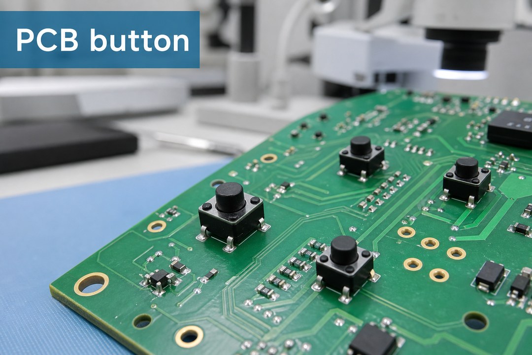
A PCB button is a button function built on or mounted to a printed circuit board. It allows a user to press a physical area or switch and send an electrical signal to the circuit.
In real products, a PCB button can appear in several forms:
- A tactile switch soldered by SMT or through-hole assembly
- A metal dome placed over PCB contact pads
- A rubber keypad pressing onto carbon or plated contacts
- A panel-mounted push button connected to the PCB
- A small board-level switch used for reset, mode selection, power, pairing, or user input
This is why buyers should not treat “PCB button” as one fixed structure. Two products may both use PCB buttons, but the manufacturing risk can be completely different.
For example, a simple reset button on an internal control board may only need a low-profile tactile switch and basic functional testing. A user-facing button on an industrial controller may require repeated pressing, stable tactile feedback, accurate enclosure alignment, strong solder joints, and contact surfaces that do not oxidize too quickly.
The first RFQ question should be:
- Is the button a soldered component?
- Is it a metal dome/contact pad structure?
- Is it part of a rubber keypad?
- Is it a panel switch connected to the PCB?
- Does the customer need PCB fabrication only, or PCB fabrication plus PCBA assembly?
When these points are clear, the PCB manufacturer can review the layout, material, surface finish, assembly process, and test plan more accurately.
PCB Button vs PCB Switch: What Should Buyers Specify?
A PCB button usually describes the user input function. A PCB switch usually describes the actual component or switching structure that opens or closes the circuit. In sourcing and manufacturing communication, the two terms are often mixed, but they should not be treated as identical.
A buyer may say, “We need a PCB button,” while the production file may actually require a tactile switch, a side-actuated switch, a metal dome array, or a through-hole push button.
What buyers should specify:
| Item | Why It Matters |
| Button type | Determines footprint, soldering, and assembly method. |
| Mounting method | SMT, through-hole, panel mount, or contact pad. |
| Actuator direction | Top-press, side-press, or enclosure-driven. |
| Height requirement | Affects enclosure fit and user feel. |
| Operating force | Affects tactile feedback and component choice. |
| Expected use | Reset, power, mode, emergency, keypad, or signal input. |
| Testing method | Continuity, functional, fixture, or product-level test. |
A common mistake is choosing a PCB switch only by size or price. In production, the better question is whether the switch matches the PCB footprint, soldering process, enclosure design, operator access, and product reliability target.
If the button will be pressed frequently, the project may need stronger solder joint control, better mechanical support, and functional testing after assembly. If the button is rarely used, such as an internal reset button, cost and space may be more important than long-term tactile feel.
How Does a Button PCB Work in Real Products?
A button PCB works by converting a physical press into an electrical signal. When the user presses the button, the circuit changes state. The product may turn on, reset, select a mode, trigger a command, or send an input signal to a controller.
But from a PCB/PCBA manufacturing point of view, the button is not just a simple on/off point. It is a mechanical-electrical interface. That interface has to survive soldering, handling, enclosure assembly, repeated pressing, vibration, and possible contamination.
A button PCB normally needs attention to:
- Copper pad shape and spacing
- Solder mask opening
- Surface finish
- Switch footprint accuracy
- Component height and orientation
- Enclosure clearance
- Cable or connector access near the button
- Test point access
- Rework possibility
- Cleaning and contamination risk
For metal dome or contact pad style buttons, the surface condition is especially important. If the pad design, plating, or cleanliness is not controlled, the button may feel correct mechanically but fail electrically after repeated use.
For SMT tactile switches, the biggest risks are usually solder bridging, insufficient solder, floating parts, shifted components, weak joints, or wrong orientation. For through-hole buttons, risks often include poor hole fit, insufficient solder fill, tilted assembly, or stress from the enclosure.
That is why button PCB projects should be reviewed as PCB + component + assembly + mechanical fit, not as a single isolated circuit symbol.
PCB Push Button Switch Options for SMT and Through-Hole Assembly
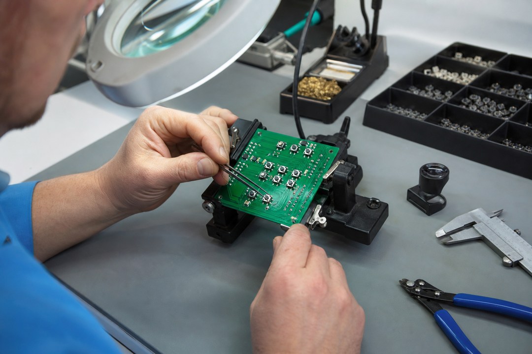
A PCB push button switch can be assembled in different ways depending on product structure, force requirement, board thickness, and production volume.
Common assembly options include:
- SMT tactile switch: compact, common for small electronics, suitable for automated placement
- Through-hole push button: stronger mechanical anchoring, useful when pressing force is higher
- Right-angle switch: useful when the user presses from the side of the enclosure
- Illuminated switch: used when the product needs both input and visual indication
- Metal dome contact: thin structure, often used in keypads and control interfaces
- Rubber keypad over PCB contacts: useful for sealed or multi-button interfaces
Each option changes the PCB and PCBA requirements.
SMT switches are efficient for automated assembly, but they need accurate stencil design, stable placement, and reflow compatibility. If the switch is too close to tall components, a shield, a housing wall, or a connector, it may be difficult to inspect or rework.
Through-hole assembly may provide stronger mechanical support, but it needs correct hole diameter, pad size, soldering method, and solder fill inspection. If the board is too thin or the switch is pressed heavily without enclosure support, the solder joints may carry too much mechanical stress.
Metal dome buttons can save height and provide a clean keypad feel, but the contact pad design, surface finish, adhesive layer, dome position, and cleanliness must be controlled carefully.
The best choice depends on the product, not only the switch price.
For a handheld tester, a low-profile SMT switch may be enough. For an industrial control panel, a through-hole or mechanically supported switch may be safer. For a sealed keypad, a metal dome or rubber keypad structure may fit better.
PCB Board Button Requirements Before Manufacturing
Before manufacturing a PCB board button project, the engineering files should make the button structure clear. If the drawing only says “button” without component details, the supplier may quote the PCB but miss assembly risks.
Project requirements should include:
- Gerber files
- BOM with manufacturer part number
- Pick-and-place file for assembly
- Assembly drawing
- Switch footprint or land pattern
- Button height requirement
- Enclosure or mechanical drawing if available
- Surface finish requirement
- Test requirement
- Expected order quantity
- Prototype or mass production schedule
If the button is part of a customer-facing interface, the mechanical drawing becomes especially important. A button may pass electrical testing but still fail in the final enclosure if the actuator is too low, too high, off-center, or blocked by a housing rib.
Another important point is panelization. If the PCB includes edge buttons, side buttons, or buttons near a cutout, the panel design must not create stress during depaneling. Poor depaneling can crack solder joints, shift components, or damage nearby pads.
For buyers, the safest approach is to send both electrical and mechanical information before quotation. This helps the supplier check not only whether the board can be made, but whether the button can be assembled, inspected, tested, and used reliably.
Circuit Board Push Button Switch Assembly Risks to Check Early
A circuit board push button switch looks simple, but it can create production problems if reviewed too late. Many issues are not found in the schematic. They appear during SMT placement, soldering, enclosure assembly, or functional testing.
Key assembly risks include:
- Wrong footprint: the switch pins do not match the PCB pads or holes.
- Wrong orientation: the actuator direction does not match the enclosure.
- Weak solder joint: the switch receives pressing force but has limited mechanical support.
- Height mismatch: the button does not reach the enclosure keycap correctly.
- Poor clearance: nearby parts block pressing, inspection, or rework.
- Solder bridging: fine switch terminals receive too much solder paste.
- Insufficient solder: the switch works at first but fails after repeated pressing.
- Flux or contamination: contact areas become unstable.
- Missing test access: the button function cannot be checked efficiently after assembly.
A real production issue often begins with one small assumption. For example, a customer may reuse a tactile switch footprint from an older project. The new switch looks similar, but the terminal spacing is slightly different. During assembly, the switch can still sit on the board, but solder wetting is uneven. The first samples may pass, while some production units later show intermittent button response.
This is exactly the type of issue that DFM and assembly review should catch before production.
EBest Circuit can help review button-related manufacturing risks from the PCB and PCBA side, including footprint consistency, soldering method, component orientation, layout manufacturability, inspection access, and test requirements.
PCB Button Reliability Checks Before Mass Production
PCB button reliability is not only about whether the button works once. It is about whether the button keeps working after repeated operation, transportation, enclosure assembly, and real product use.
For prototype orders, the main goal is usually to confirm function and mechanical fit. For small-batch or production orders, the focus should move toward repeatability.
Important review points include:
- Does the button align with the enclosure opening?
- Does the switch height match the mechanical design?
- Is the switch protected from excessive pressing force?
- Are the pads strong enough for repeated operation?
- Is the surface finish suitable for the contact structure?
- Can AOI or visual inspection see the solder joints?
- Does the test fixture confirm button response?
- Is rework possible without damaging nearby components?
- Are the switch and PCB process compatible with lead-free reflow?
- Does the assembly drawing clearly show polarity or orientation?
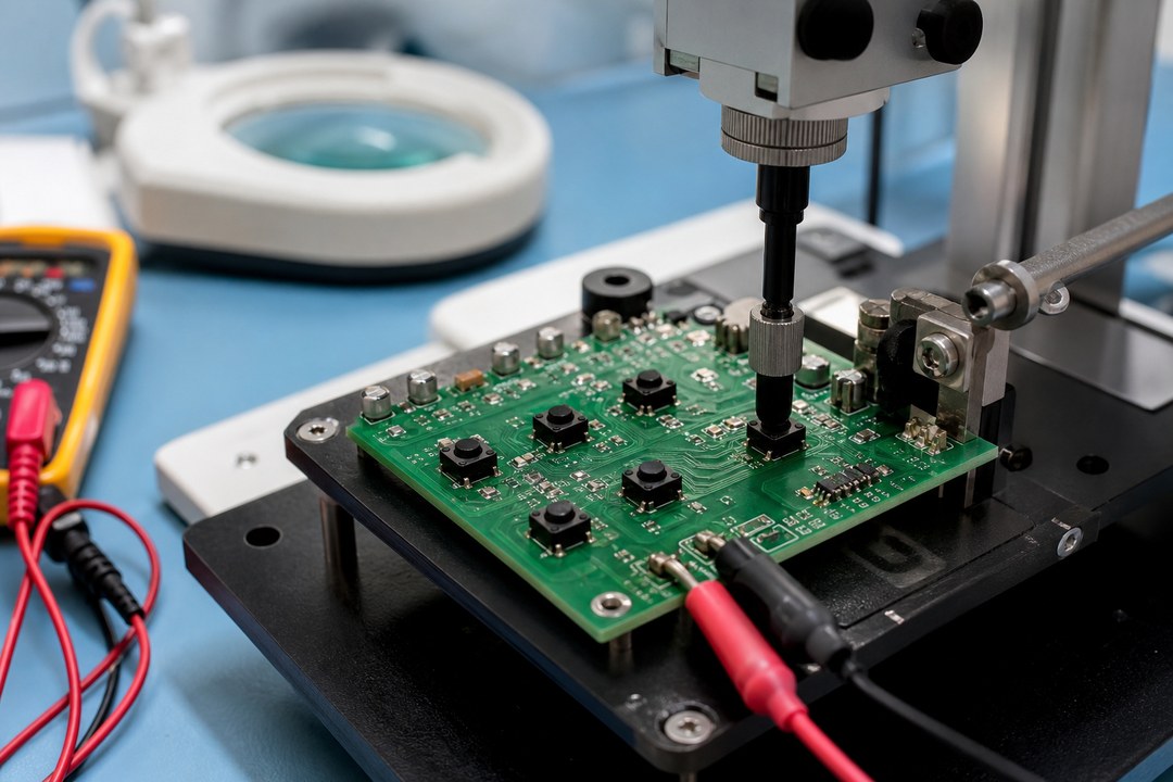
For contact pad or metal dome style PCB buttons, surface finish and cleanliness deserve extra attention. ENIG, hard gold, carbon contacts, or other contact finishes may be considered depending on the product requirement, but the final selection should be confirmed based on use conditions and manufacturer capability.
For tactile switch assembly, the focus is usually solder joint quality, placement accuracy, reflow profile compatibility, and mechanical stress after enclosure installation.
A good production plan should define what is checked at incoming material, SMT/THT assembly, visual inspection, functional testing, and final packing. Without this plan, button failures may only appear after the product is assembled into the housing, when repair becomes much slower and more expensive.
How EBest Circuit Supports PCB Button PCB and PCBA Projects
EBest Circuit (Best Technology) supports PCB button projects by reviewing the manufacturing and assembly details that affect real production quality. The goal is not to replace the customer’s product design team, but to help make approved PCB files easier to manufacture, assemble, inspect, and test.
EBest Circuit supports PCB button projects with:
- PCB fabrication for prototype, small-batch, and production orders
- PCB layout manufacturability review
- DFM review before production
- BOM and component sourcing coordination
- SMT assembly
- Through-hole assembly
- Mixed SMT and THT assembly
- Inspection support such as AOI, visual inspection, and solder joint checks
- Functional testing support according to customer requirements
- One-stop PCB and PCBA service for engineering teams
For button PCB projects, EBest Circuit can help check whether the switch footprint matches the BOM, whether the assembly drawing is clear, whether the button position may create soldering or inspection risk, and whether the project should use SMT, through-hole, or mixed assembly.
This is useful for engineers who already have product design files but need a manufacturing partner to help turn those files into reliable boards and assembled PCBAs.
If the project includes uncertain component availability, EBest Circuit can also help review sourcing options and communicate with the customer before production. This reduces the risk of replacing a switch with a “similar” part that does not match the footprint, height, actuator direction, or production process.
For project review, send Gerber files, BOM, pick-and-place file, assembly drawing, and any enclosure or test requirement to sales@bestpcbs.com.
PCB Button Project Example for an Industrial Control Panel
A practical PCB button project may look simple at the RFQ stage, but the details decide whether production is smooth.
A customer developing an industrial control panel needed a small PCBA with several user-input buttons, indicator LEDs, and connectors. The first prototype used SMT tactile switches because the product needed a compact board size and automated assembly. The electrical function was simple, but the mechanical use condition was not: operators would press the buttons repeatedly while wearing gloves, and the board would be fixed behind a plastic front panel.
Project requirements:
- Application: industrial control panel
- Board type: FR4 PCB with SMT assembly
- Key components: tactile switches, LEDs, connectors, resistors, controller-related components supplied by customer BOM
- Order stage: prototype PCB assembly validation before small-batch production
- Main concern: button alignment, solder joint strength, and functional testing
- Delivery goal: fast prototype build for enclosure trial
During manufacturability review, several issues needed attention.
The first issue was switch height. The selected tactile switch was close to the required height, but the enclosure keycap tolerance was not clearly shown. If the switch sat slightly lower after soldering, the user might feel weak feedback. If it sat too high, the button might be partially pressed after enclosure assembly.
The second issue was component clearance. Two connectors were placed close to the button area. Electrically, the layout worked. Mechanically, the operator’s pressing direction and enclosure ribs could make inspection and rework difficult.
The third issue was soldering repeatability. The switch pads were small, and too much solder paste could cause uneven seating. Too little paste could create weak joints. The stencil opening and placement accuracy needed to be controlled for the prototype.
The fourth issue was testing. The customer originally planned only a visual check, but visual inspection could not confirm whether every button triggered correctly after assembly. A simple functional test was added to confirm button response before packing.
EBest Circuit solution:
- Reviewed the switch footprint against the BOM
- Checked button position and assembly direction
- Confirmed SMT assembly process for the tactile switches
- Flagged mechanical clearance points for customer confirmation
- Supported PCBA assembly and functional testing based on customer files
- Helped the customer prepare the prototype for enclosure validation
This kind of project shows why a PCB button should be reviewed as part of the full product build. The circuit may be simple, but the final success depends on PCB layout, component match, assembly control, enclosure fit, and test coverage.
FAQs About PCB Button
What is a PCB button?
A PCB button is a button function built on or mounted to a printed circuit board. It may use a tactile switch, metal dome, contact pad, rubber keypad, or push-button switch structure.
Is a PCB button the same as a PCB switch?
Not always. A PCB button usually describes the user input function, while a PCB switch describes the switching component or structure used to create that function.
Can EBest Circuit manufacture PCB button boards?
Yes. EBest Circuit can support PCB fabrication, DFM review, component sourcing coordination, PCBA assembly, inspection, and testing support for PCB button projects based on customer-approved files.
What files are needed for a PCB button PCBA quote?
Gerber files, BOM, pick-and-place file, assembly drawing, switch part number, button height requirement, surface finish requirement, and test requirement are recommended.
What causes PCB button failure after assembly?
Common causes include wrong footprint, poor solder joints, wrong switch orientation, enclosure interference, weak mechanical support, contamination, poor contact pad design, or missing functional testing.
In Conclusion, a PCB button may be small, but it connects electrical design, PCB fabrication, component sourcing, PCBA assembly, mechanical fit, and final user experience. To avoid production delays or unreliable button response, buyers should define the switch type, footprint, height, surface finish, assembly method, and test requirement before manufacturing.
EBest Circuit (Best Technology) supports PCB and PCBA projects that need reliable button assembly, DFM review, sourcing coordination, inspection, and testing support. If you need help reviewing a PCB button project before prototype or production, contact sales@bestpcbs.com.