Star grounding is a targeted fix for shared-return noise, not a default PCB layout style. It helps when a known high-current or noisy load would otherwise share return copper with a sensitive circuit, and the two branches can meet at one short, controlled junction. Fast digital, RF, and widely distributed currents usually need a continuous ground plane instead.
A sound choice starts with the actual current loops: identify the disturbing current, the reference that must stay quiet, the fastest edge, and every path that can reconnect the grounds. Those four facts lead to a practical decision between a star, a plane, or a hybrid layout and define what must be measured on the prototype.
What Is Star Grounding, and What Problem Does It Solve?
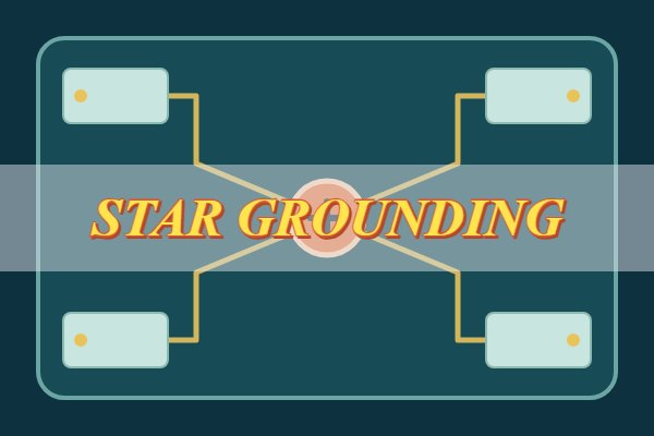
Star grounding gives selected circuits separate return branches that meet at one controlled junction. The aim is to stop current from one branch flowing through the reference used by another branch before both currents reach their common source.
The problem is common-impedance coupling. Copper, vias, connectors, and solder joints all have impedance. When two circuits share a return segment, the current from the first circuit creates a voltage across that segment:
Reference error = shared return current × shared-path impedance
Consider a 24 V control board with a solenoid and a sensor amplifier. If the solenoid and amplifier share return copper, each solenoid current step can shift the amplifier reference and appear as a false sensor signal. Separate branches can keep the solenoid current out of the measurement path until both returns reach the supply reference.
The topology is useful only when the designer can name both sides of that relationship: the current that causes the error and the reference it disturbs. A radial drawing without that explanation is not a design decision.
How Do Frequency and Return Paths Affect Star Grounding?
Low-frequency load currents may tolerate separate branches, while fast-edge currents need a short return close to the outgoing signal. This is why a star can reduce sensor-reference error yet make a clock, data bus, or switching node worse.
Nominal operating frequency is not enough. A slowly updated bus may still switch in nanoseconds, and a low-sample-rate converter may contain fast clocks. Long branches add inductance and loop area, which can increase ringing, crosstalk, emissions, and susceptibility even when their DC resistance looks acceptable.
Check three things for every important signal or load:
- The complete loop: source, outgoing conductor, load, and return conductor.
- The fastest transition: driver rise and fall time, switch-node edge, converter clock, or ESD event.
- Return continuity: plane splits, narrow necks, missing return vias, and connector boundaries that force a detour.
If a proposed branch sends a fast return across the board before it can close, use a nearby plane for that loop. The same PCB can still use a dedicated branch for a compact low-frequency load return.
When Does Star Grounding Work Well?
Star grounding works well when one identifiable load threatens one identifiable reference and both branches can reach a compact junction. The following conditions should all be true:
- The disturbing current is known. Typical sources include a relay, motor, solenoid, heater, lamp, or power-output stage.
- The sensitive reference is known. It may belong to a sensor, precision reference, measurement shunt, low-level audio input, or feedback network.
- The junction is physically close. A supply return, bulk-capacitor return, regulator return, or connector boundary can accept the branches without long radial routing.
- Fast local loops stay local. Decoupling, clocks, interfaces, and switching loops still close through a nearby plane or tightly coupled conductor pair.
On the control-board example, the solenoid can return directly to the power-entry capacitor while the sensor branch reaches the same reference on separate copper. The ADC and microcontroller interface can remain over continuous ground. This is a hybrid solution driven by current paths, not by the labels “analog” and “digital.”
When Should You Avoid Star Grounding and Use a Ground Plane Instead?
Avoid a whole-board star when fast signals, RF energy, dense routing, or distributed loads need many short return paths. Start with a continuous ground plane for most multilayer digital boards, then add a controlled junction only where a specific noisy branch must be kept out of a sensitive region.
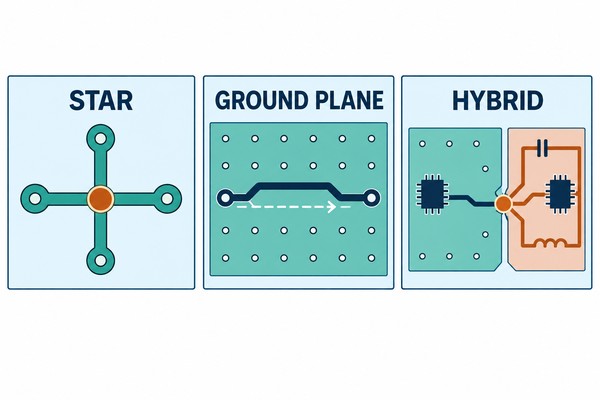
| Board condition | Starting topology | What to verify |
|---|---|---|
| One compact low-frequency load beside a sensitive reference | Star or Kelvin return | Measure reference movement during the worst load step. |
| Clocks, fast buses, RF traces, or rapid converter interfaces | Continuous ground plane | Keep an adjacent return path beneath the complete signal route. |
| Fast local interfaces beside a noisy power section | Hybrid | Keep fast returns on the plane and control where the power return joins it. |
| Loads spread across a large board | Plane or region-based power return | Calculate voltage differences using the actual routing length and current. |
| Several boards, cables, shields, or conductive mounts | System-level grounding plan | Trace every connection that can create a parallel return path. |
A layout should be judged by return-current behavior rather than visual symmetry. A neat radial pattern can create a large high-frequency loop, while careful placement over a solid plane can keep a noisy load current away from a measurement circuit.
Where Should the Star Ground Point Be Placed?
Place the star point where the selected branch currents return to their shared source without crossing another branch’s reference first. That point is often near a bulk capacitor, regulator return, supply connector, or measurement shunt, not at the geometric center of the PCB.
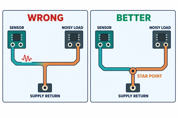
- Mark the sources and loads. Include connectors, regulators, bulk capacitors, switching stages, sensors, converters, and external cables.
- Draw outgoing and return current together. Check steady load, the worst load step, and the fastest transition because the paths may differ.
- Locate the protected reference. Identify the exact point where the sensor, amplifier, ADC reference, or feedback network measures voltage.
- Join the branches after their local reference points. The noisy current should reach the shared source without using the sensitive branch’s copper.
A net tie or zero-ohm resistor can make the chosen junction visible in the schematic and testable on the board. It cannot correct long branches or poor placement. Choose the electrical location first, then use the component or copper feature to enforce it.
How Should Analog, Digital, Power, and Chassis Grounds Meet?
Connect ground regions according to the currents they carry and the reference required by signals that cross between them. The names AGND, DGND, PGND, and chassis ground describe roles; they do not automatically require separate copper planes.
- Analog return: keep load and switching current away from low-level inputs, references, and feedback nodes.
- Digital return: give clocks and interfaces a short path beside their signal traces, even when average current is small.
- Power return: contain converter hot loops, motor current, and gate-drive current near their sources and local capacitors.
- Chassis, shield, and protective earth: route ESD, common-mode, shield, and safety current at the connector or enclosure boundary without sending it through a sensitive reference.
For a mixed-signal IC, follow the device data sheet and reference layout before splitting ground. AGND and DGND pins may describe internal circuit functions rather than a requirement for two board planes. The relevant questions are where the pin currents flow and what reference the crossing signals use.
Also trace paths outside the PCB. A cable shield, metal standoff, programming lead, or oscilloscope earth connection can bypass the intended junction. A board-level star is valid only if the assembled system preserves it.
What Layout Mistakes Make Star Grounding Fail?
Star grounding fails when the copper, components, or external connections create a different current path from the one shown on the schematic. These mistakes are the first places to look when the expected noise reduction does not appear:
- The junction is beyond the sensitive reference. The noisy current crosses the measurement reference before reaching the star. Move the junction or change placement.
- The branches are too long. A branch with acceptable DC resistance can still have excessive inductance. Keep fast returns on a plane.
- A signal crosses a split or narrow ground neck. The return detours around the gap. Reroute the signal or restore continuous ground beneath it.
- A second connection bypasses the star. Noise changes when a cable, enclosure, debugger, or instrument is attached. Trace current through the complete test setup.
- Decoupling current travels to a remote junction. The IC supply loop becomes larger than necessary. Close each high-frequency decoupling loop locally.
- A bead or zero-ohm link replaces analysis. The fitted part adds impedance but does not define the current path. Select it only after the target current and allowed voltage difference are known.
Change one path at a time during troubleshooting. Switch the suspected load while monitoring the protected reference, then repeat with the enclosure and external cables connected. The difference separates shared-copper error from a secondary path or radiated-coupling problem.
How Can You Review and Test a Star Ground Design?
A star-ground design is ready when the current-path drawing, physical junction, and measured result agree with one defined acceptance limit. Six checks provide that evidence:
- Draw the critical loops. Mark the source, outgoing path, load, return, and local decoupling loop for each noisy, fast, or sensitive circuit.
- Name the coupling. Record the aggressor current, shared path, victim reference, operating condition, and maximum acceptable error.
- Compare the drawing with the PCB. Check branch length, plane continuity, layer changes, connectors, shields, mounts, and the exact junction feature.
- Estimate the low-frequency error. Calculate shared resistance and voltage drop at maximum load and compare the result with the allowed reference shift.
- Measure the load event. Compare idle and worst-load conditions with a short-ground-spring probe or an appropriate differential probe. Save the waveform that occurs at the same time as the disturbing event.
- Repeat the test on the assembled system. Add the enclosure, shields, cables, debugger, and representative external equipment so hidden return paths are included.
The result should lead to one decision. Keep the star if the protected reference stays within its limit and fast local returns remain continuous. Use a plane or hybrid if fast or distributed currents need a nearby reference. Change the architecture if the current paths or acceptance limit are still unclear.
FAQs About Star Grounding
Q1: Should each star-ground branch use a separate schematic net name?
A1: Use separate net names when they help the CAD tools enforce the intended connection. Join them with a documented net tie or approved junction footprint, then confirm that the PCB netlist and copper contain no unintended second connection.
Q2: How wide should a star-ground branch be?
A2: Size it from current, allowable voltage drop, temperature rise, and transient behavior. There is no universal width. A high-current branch may need wide copper, while a sensing branch may need a separate Kelvin path that carries almost no load current.
Q3: Can a ground pour surround star-ground branches?
A3: Yes, but the pour must not create a parallel connection between branches. Use clearances or a controlled net-tie strategy, then inspect the final Gerber data and connectivity report rather than relying on the schematic alone.
Q4: Can several regulators share one star point?
A4: They can when their return currents meet at a low-impedance source node without modulating another regulator’s reference. If one converter has large switching or load-step current, give it a local hot loop and check whether a higher-level junction is needed.
Q5: How should star-ground noise be measured with an oscilloscope?
A5: Measure between the protected reference and its source reference during the suspected load event. Use a short ground spring or a suitable differential probe; a long probe ground lead can create a loop and show noise that is not present at the circuit node.
Conclusion: Choose the Grounding Topology from the Current Loops
Choose a star only for a specific shared-impedance problem that has short branches, a clear victim reference, and one practical convergence point. Choose a continuous plane when fast or distributed currents need nearby returns. Use a hybrid when those two needs exist on the same board.
The next design review should produce two items: an annotated drawing of the critical current loops and a measurement plan for the worst load event. If both are specific, the topology choice can be checked. If either remains vague, deciding between star grounding and a ground plane is premature.