A laser diode driver board converts a power supply and control command into accurately regulated diode current. A reliable board must do more than turn the laser on: it must limit current, control startup and shutdown, suppress electrical transients, manage heat, and provide testable interfaces. This guide connects those operating requirements to circuit design, PCB layout, prototyping, fabrication, assembly, inspection, and quotation preparation.
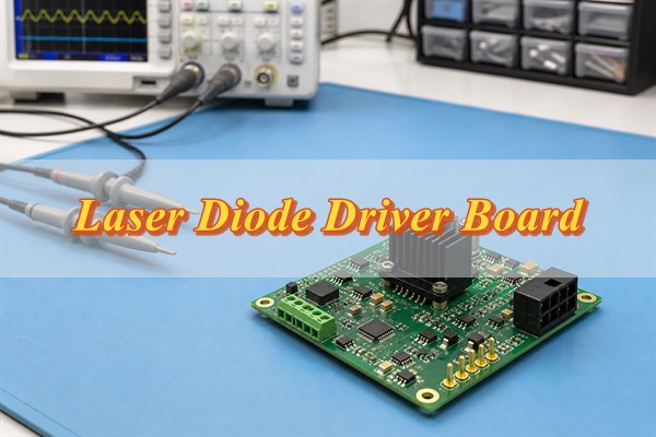
What Is a Laser Diode Driver Board and What Does It Do?
The board regulates laser-diode current and provides protection. It receives DC power and an enable or modulation command, then regulates the diode current within the limits defined by the application. Depending on the system, it may also monitor optical power, diode voltage, temperature, interlock status, or fault conditions.
The board normally includes a control stage, a current-sense element, a power stage, local energy storage, connectors, and protection circuitry. It may be a small embedded PCB inside an instrument or a larger assembly that interfaces with a separate laser head and temperature controller. The wavelength printed on a laser diode does not determine the driver by itself; the electrical and thermal operating envelope does.
How Does a Laser Diode Driver Circuit Board Work?
The circuit board converts a control command into regulated laser-diode current. A feedback loop measures the actual output, compares it with the target value, and adjusts the power stage until the error is reduced. This closed-loop action keeps the current or optical output within the operating range defined for the laser and application.
In constant-current operation, a sense resistor produces a voltage proportional to diode current. The controller compares this feedback voltage with the command reference, then drives a transistor, linear stage, or switching stage to correct the difference. The sense path, reference accuracy, power-stage response, and loop compensation determine regulation stability and transient behavior.
In constant-power operation, the laser package’s monitor photodiode provides feedback related to optical output. The controller adjusts diode current to maintain the commanded optical level. This method requires the correct photodiode polarity, a defined calibration range, stable compensation, and limits that prevent the control loop from increasing current beyond the diode’s safe boundary.
Protection functions operate around the main feedback loop. Soft-start controls the initial current rise; a hardware current clamp limits an excessive command; enable and shutdown logic define safe sequencing; and open-load, reverse-voltage, or interlock protection addresses abnormal conditions. These functions must be evaluated during startup, normal modulation, shutdown, and connector faults—not only under steady-state operation.
Which Laser Diode Driver Board Is Suitable for CW, Pulsed, or Modulated Operation?
Select the board from the required current waveform. Continuous-wave operation emphasizes low noise, drift, compliance voltage, and thermal stability. Pulsed operation adds peak current, pulse width, repetition rate, rise and fall time, duty cycle, energy storage, and overshoot limits. Analog modulation requires small-signal bandwidth and linearity, while TTL control requires defined logic thresholds and predictable enable timing.
Before selecting or designing the board, document normal current, absolute maximum current, forward-voltage range across temperature, grounded-anode or grounded-cathode configuration, modulation source, allowed optical response, and the maximum acceptable transient. A board described only as “high power” or “fast” is not sufficiently specified.
| Operating Requirement | Verify in the Driver Specification | PCB and PCBA Design Focus |
| CW output | Continuous current range, compliance voltage, current noise, drift, and worst-case dissipation | Low-noise sensing and references, continuous heat removal, and adequate copper and connector current capacity |
| Pulsed or QCW output | Peak current, pulse width, repetition rate, duty cycle, rise and fall time, and permitted overshoot | Minimum high-di/dt loop area, local pulse-energy storage, controlled switching returns, and low-inductance measurement access |
| Analog modulation | Input range, transfer function, bandwidth, linearity, bias point, and output-current limits | Stable control and return paths, separation from switching nodes, and connectors and test access suitable for the required bandwidth |
| Digital enable or gating | Logic thresholds, propagation delay, minimum on/off time, default state, and interlock behavior | Defined logic reference, input protection, noise immunity, and safe power-up and power-down sequencing |
Where Are Laser Diode Driver Boards Used in Optical and Laser Systems?
Laser diode driver boards are selected from the optical function and its required current waveform. The application determines whether the PCB must prioritize low noise, pulse integrity, synchronization, thermal stability, compact integration, or repeatable production testing.
- Fiber-optic communication: The driver supplies a controlled bias current and, when required, a modulation current to an optical transmitter. Define the average and modulation current, compliance voltage, modulation bandwidth, connector or package interface, allowed noise, and temperature range. PCB review should focus on the signal return path, power-supply noise, impedance-controlled interfaces where required, and heat removal from the laser and driver stage.
- LiDAR and time-of-flight sensing: The board generates repeatable current pulses used to illuminate a scene before the receiver measures return timing. Specify peak current, pulse width, repetition rate, duty cycle, rise and fall time, permitted overshoot, laser connection, and trigger timing. The PCB requires a compact high-di/dt loop, local pulse-energy storage, controlled switching return paths, and measurement access that does not add excessive inductance.
- Machine-vision illumination: The driver synchronizes a laser line, spot, or structured-light source with a camera or motion event. Provide the trigger voltage, trigger polarity, delay, exposure window, pulse current, duty cycle, and maximum junction or case temperature. Manufacturing review should confirm connector polarity, logic-input protection, repetitive thermal load, and a production test that verifies trigger-to-output timing.
- Spectroscopy and gas sensing: The board controls laser current while the instrument measures absorption or another wavelength-dependent response. Define the current scan or modulation waveform, bandwidth, noise limit, temperature-control interface, monitor-photodiode connection, and calibration points. Layout should separate quiet sensing and reference nodes from switching current, while the test plan should verify drift and waveform accuracy under the specified thermal conditions.
- Interferometry and precision metrology: The driver supports a stable optical source for displacement, vibration, dimensional, or phase-sensitive measurement. Submit current-noise, drift, modulation, grounding, shielding, and warm-up requirements. PCB and PCBA review should protect low-level feedback paths from shared impedance and EMI, and production testing should use defined settling time and measurement bandwidth.
- Medical and laboratory instruments: The driver provides controlled laser current inside diagnostic, analytical, therapeutic, or research equipment. The product owner must define the laser limits, interlock behavior, fault response, temperature monitoring, calibration responsibilities, and system-level safety requirements. The PCBA quotation should state which electrical protections and functional tests are included; optical alignment, laser classification, and finished-device compliance must not be assumed.
- Barcode scanning, printing, and marking: The board repeatedly switches or modulates the laser according to scan, print, or marking commands. Define repetition rate, modulation depth, on/off timing, expected operating hours, connector life, and thermal duty. Manufacturing priorities include repeatable component placement, robust connectors, controlled heat transfer, and an end-of-line test covering output timing and current limits.
- Industrial alignment and measurement: The driver operates a laser used for positioning, leveling, dimensional inspection, or process monitoring. Specify the input-voltage range, current setting, enable interface, cable length, ambient range, enclosure cooling, ESD exposure, and service procedure. The PCB design should provide protected external interfaces, mechanically supported connectors, accessible test points, and traceable configuration control for replacement assemblies.
For quotation, convert the application into measurable electrical, timing, thermal, mechanical, and test limits. This allows the PCB/PCBA manufacturer to review the actual current paths, stackup, component footprints, assembly risks, connectors, inspection coverage, and fixture requirements instead of pricing from an application name alone.
What Causes a Laser Diode Driver Board to Fail?
Uncontrolled current and stored energy cause the highest risks. Other causes include unstable feedback, heat, ESD, and incomplete interfaces. A laser diode can be damaged by a short transient even when the average current appears acceptable, so a bench supply setting alone is not a complete protection strategy.
- Startup overshoot: The reference, enable signal, and supply rails can become valid in the wrong order, briefly commanding more current than the steady-state setting. A prototype may appear stable after startup while the first microseconds contain the damaging event. Capture output current and voltage from power application through the end of soft-start, including repeated cold and warm starts.
- Loop instability: Compensation that ignores the power stage, diode model, cable, output capacitance, and PCB parasitics can produce oscillation or ringing. Symptoms include current ripple, inconsistent pulse shape, unexpected heating, or a waveform that changes when the cable or probe is moved. Evaluate stability with the intended load, connection length, operating points, and measurement method.
- Open-load energy: If the laser is disconnected while energy remains in an inductor, capacitor, or cable, the output node can rise or ring beyond its intended range. Reconnection can then deliver a stored-energy pulse to the diode. Open-load behavior should be observed during enable, steady operation, shutdown, and connector interruption using a protected test setup.
- Reverse electrical stress: Supply sequencing, cable inductance, charged capacitors, or an undefined discharge path can apply reverse voltage across the laser diode. This fault may occur during shutdown or cable removal rather than normal operation. Measure both diode polarities during power-up, power-down, fault clearing, and any permitted connection sequence.
- Thermal drift and overstress: Power semiconductors, current-sense resistors, references, connectors, and copper paths change temperature during operation. Their electrical change can shift the regulated current or reduce component margin even when the board still functions. Test the defined current and duty cycle until temperature stabilizes, then compare current accuracy and component temperatures with the approved limits.
- Assembly and component errors: Reversed components, incorrect resistor values, unapproved substitutions, insufficient thermal-pad solder, contamination, or damaged connectors can change the current path or feedback ratio. These faults may pass a basic power-on check. Inspection should combine revision and BOM verification with polarity checks, workmanship inspection, resistance checks, and functional testing at controlled current levels.
- ESD and connector transients: Handling, mating, or a cable connected between different ground potentials can inject a fast transient into the diode or control interface. Damage may be immediate or appear later as unstable output. Review the complete handling and connection path—from receiving and assembly through test, installation, and service—rather than treating the bench as the only ESD-controlled point.
- Misleading measurements: Long oscilloscope probe grounds, excessive probe capacitance, an unsuitable dummy load, or insufficient instrument bandwidth can create or hide ringing. Record the load model, probe, connection geometry, bandwidth limit, and test point used for acceptance. Production and engineering results are comparable only when the measurement setup is controlled.
How Should Current Regulation and Laser Diode Protection Be Designed?
Design current regulation and protection from one documented operating envelope. The circuit must control normal current accurately while remaining within the approved diode and component limits during startup, modulation, shutdown, open load, short circuit, connector interruption, and control faults.
- Define the safe operating envelope: Record the normal and absolute-maximum diode current, forward-voltage range across temperature, permitted reverse voltage, CW or pulse limits, duty cycle, modulation range, monitor-photodiode limits, and thermal conditions. These values become design limits; they must not be inferred from the driver rating alone.
- Select the regulation method: Choose constant-current or constant-power control and define how the command reference is generated. For constant current, establish the sense-resistor value, measurement range, accuracy, power rating, and Kelvin connection. For constant power, also define monitor-photodiode polarity, current range, calibration, and a separate maximum laser-current boundary.
- Design the feedback loop: Select the amplifier, power stage, compensation network, output capacitance, and operating bandwidth as one loop. Include the laser model, cable, connector, PCB parasitics, and operating-point range in the stability review. A loop that is stable with a resistor on the bench may behave differently with the final laser connection.
- Add an independent hardware current limit: Set a clamp that prevents the command path or firmware from requesting current beyond the approved boundary. Define threshold tolerance, response time, reset behavior, and what happens if the sense signal is missing or implausible. The limit circuit must be reviewed across component tolerance and temperature.
- Control startup and shutdown: Coordinate supply rails, reference generation, enable logic, soft-start, output discharge, and interlock status. The laser current should remain disabled until required rails and control signals are valid, then rise according to a defined ramp. Shutdown must remove stored energy without applying a reverse or reconnect pulse.
- Protect abnormal output conditions: Define the response to open load, short circuit, reverse connection, cable interruption, and connector mating. Depending on the circuit, protection can include voltage clamps, reverse-current paths, controlled discharge, output shorting while disabled, fault latching, or a requirement that connections be made only when de-energized.
- Separate hardware and firmware responsibilities: Use hardware for faults that can damage the diode faster than software can detect and respond. Firmware can supervise temperature and interlocks, manage sequencing, record faults, and require an operator reset, but its timing and failure modes must be documented if it participates in a protective action.
- Verify the complete fault matrix: Test minimum, nominal, and maximum input voltage; cold and hot startup; normal modulation; commanded shutdown; open load; short circuit; interrupted connection; and loss of control or feedback signals. Record current and voltage at the diode interface with a specified load and probe method, then compare every transient with the approved limits.
The released design package should state the protection thresholds, tolerances, timing requirements, reset behavior, test points, loads, instruments, and acceptance limits. This gives prototype and production teams one repeatable basis for functional testing instead of relying on a visual inspection or a steady-state current reading.
Which PCB Materials and Stackups Are Suitable for Laser Diode Driver Boards?
Use multilayer FR-4 when it meets the verified current, temperature-rise, signal-integrity, and assembly requirements. Move to high-Tg FR-4, an insulated metal substrate, metallized ceramic, or a low-loss hybrid only when the design has a specific limitation that standard FR-4 cannot meet. The limitation should be demonstrated by thermal analysis, electrical calculation, prototype measurement, assembly exposure, or a documented reliability requirement.
Release the stackup before final routing. The stackup should define each layer’s function, approved core and prepreg family, finished thickness, copper weight, dielectric spacing, reference planes, via structure, and any controlled-impedance requirement. For high-current paths, verify copper width, allowable temperature rise, via current sharing, connector capacity, and the complete path to the return. For heat-producing components, identify how heat moves from the component pad through copper and vias to the chassis or heatsink.
Material upgrades must solve the identified constraint without creating a new fabrication or assembly risk. High Tg does not by itself provide high thermal conductivity; an IMS may restrict routing and isolation options; ceramic changes mechanical and assembly requirements; and low-loss material should be limited to nets that need its dielectric performance. The quotation package should therefore include the proposed stackup, critical current paths, thermal interface, impedance table when applicable, and acceptable material alternatives.
| Construction Option | Use When | Verify Before Release |
| Standard or multilayer FR-4 | The control, regulation, routing density, electrical loss, and measured temperature rise remain within the design limits | Approved laminate, finished thickness, copper weight, dielectric spacing, via current, plane continuity, and board-to-chassis thermal path |
| High-Tg FR-4 | Assembly exposure or laminate reliability requires greater thermal robustness; high Tg alone is not evidence of better heat spreading | Tg test method, decomposition temperature, Z-axis expansion, delamination resistance, applicable temperature rating, and thermal conductivity as separate properties |
| Insulated metal substrate | Heat must conduct through an electrically isolating dielectric into a metal base and the required circuit structure is compatible with the selected IMS system | Dielectric thermal impedance and isolation, copper and base thicknesses, supported layer structure, creepage and clearance, and mechanical contact to the final heatsink |
| Metallized ceramic substrate | Power density, electrical isolation, thermal conductivity, or coefficient-of-expansion requirements justify DBC, AMB, or another qualified ceramic process | Ceramic type, copper and ceramic thicknesses, conductor spacing, metallization process, assembly method, mechanical stress, reliability plan, and cost |
| Low-loss or hybrid laminate | Identified high-frequency paths require controlled dielectric loss or phase behavior; a fast edge alone does not justify changing the whole board material | Dk and Df at the relevant frequency, copper profile, impedance structure, hybrid-material transitions, fabrication controls, and material availability |
How Should a Laser Diode Driver PCB Layout Reduce Overshoot, Noise, and EMI?
Lay out the board in current-flow order, starting with the fastest and highest-current loop. Each routing decision should reduce loop area, shared return impedance, unwanted coupling, or measurement uncertainty.
- Place the pulsed power loop first: Put the local energy-storage capacitor, switching device, laser connector, and return close together. Route the outgoing and return paths as a compact pair instead of sending pulse current through general power or ground routing.
- Connect local energy storage directly: Place the pulse or high-frequency bypass capacitor at the power-stage terminals it supports. Use short, wide connections and sufficient vias so transient current does not arrive through a long supply path.
- Limit the switching-node area: Use only the copper required for current capacity, voltage spacing, and heat spreading. Keep this node away from the current-sense pair, reference, modulation input, interlock, and connector signals.
- Route the current-sense pair as a Kelvin connection: Take both traces directly from the sense-resistor terminals, route them together, and connect them only to the feedback amplifier input. Do not share these traces or vias with load current.
- Preserve the return path: Provide a continuous reference plane beneath fast control and modulation signals. Avoid plane splits, slots, antipads, and connector voids that force return current around a longer path.
- Separate quiet and noisy circuits: Keep the reference, feedback amplifier, and low-level control circuitry away from the switch node and gate-drive loop. Join power and signal returns only at the points defined by the circuit architecture.
- Include the laser connection in the loop review: Check connector pin order, cable length, polarity, shielding, and return conductors. A compact PCB loop can still ring when the external connection adds inductance or an undefined return path.
- Add controlled measurement access: Provide signal-and-ground test points for current, output voltage, enable, and fault signals. Keep probe loops short and document the intended probe or fixture so engineering and production results are comparable.
Before release, mark the startup, CW, pulse, modulation, fault, and discharge current paths on the PCB. Confirm that each path has a defined source, return, protection element, and measurement point.
How Should Thermal Management Be Designed for a Laser Diode Driver Board?
Design a complete thermal path from every heat-generating component to the surrounding air, chassis, or heatsink. Base the design on worst-case electrical loss and operating conditions rather than copper area alone.
- Calculate the heat at each source: Estimate conduction and switching loss in the power device, controller loss, and sense-resistor dissipation. Use maximum current, voltage drop, switching frequency, duty cycle, input voltage, and component tolerance for the intended operating mode.
- Define the maximum operating temperature: Record the highest ambient and enclosure temperatures, airflow condition, operating duration, and allowable component junction or case temperature. Apply design margin instead of using the absolute maximum rating as the normal target.
- Build the package-to-board thermal path: Connect exposed pads and power terminals to adequate copper with solder coverage appropriate to the package. Use thermal vias to transfer heat into internal or opposite-side copper when one surface cannot provide sufficient spreading area.
- Size copper and thermal vias for the actual load: Review copper thickness, spreading area, via diameter, via count, plating, layer connection, and solder-wicking risk together. A large top-layer pour is not sufficient when heat cannot move through the package joint or into the rest of the board.
- Protect temperature-sensitive circuitry: Keep the current-sense resistor, reference, feedback amplifier, and temperature-monitoring components away from hot power devices and concentrated airflow exhaust. Avoid shared copper paths that transfer both load current and heat into precision circuitry.
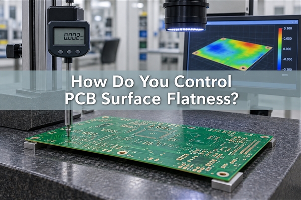
- Coordinate the PCB with the enclosure: Define whether heat leaves through natural convection, forced air, a chassis contact, or a dedicated heatsink. Specify interface-material thickness, contact area, mounting pressure, fastener location, insulation, and flatness when the board transfers heat mechanically.
- Verify the assembled board thermally: Test the prototype at worst-case current, duty cycle, ambient condition, and enclosure configuration. Measure the power device, sense resistor, nearby reference circuitry, connectors, and board hot spots after temperatures stabilize, then compare the results with the design limits.
Release the board only after the thermal test identifies the operating condition, measurement locations, stabilization criterion, acceptance limits, and any required derating.
How Is a Laser Diode Driver Board Prototyped and Validated?
Validate the prototype in controlled stages before connecting the production laser diode. The sequence should expose assembly errors, unsafe output states, unstable regulation, transient stress, and thermal limits without placing the laser at unnecessary risk.
- Confirm the prototype identity: Match the PCB revision, assembly drawing, BOM, firmware, jumper settings, and test procedure. Record any rework or substituted component before applying power.
- Inspect the assembled board: Check component polarity, laser-output connector orientation, solder joints, exposed-pad soldering, contamination, shorts, opens, and unintended resistance between power rails and ground.
- Power the board in a safe state: Use a current-limited laboratory supply with the driver disabled and the command set to zero. Verify rail voltages, reference voltages, quiescent current, enable logic, and output voltage before activating the power stage.
- Connect a representative dummy load: Use a protected load or diode emulator rated for the required current, pulse energy, and transient conditions. Document its forward-voltage behavior and connection inductance so results can be compared between tests.
- Increase output in controlled steps: Begin below the intended operating current, verify regulation accuracy and current-limit behavior, and then raise the command through defined checkpoints. Stop immediately if the waveform, supply current, or component temperature exceeds its test limit.
- Measure dynamic behavior correctly: Capture startup, shutdown, enable transitions, modulation edges, overshoot, ringing, and settling time with a low-inductance probing method. Test the actual connector and cable arrangement because they form part of the output loop.
- Exercise every protection state: Verify open-load, short-circuit, interlock, undervoltage, overtemperature, command-loss, and emergency-shutdown responses that apply to the design. Record the peak current or voltage, shutdown delay, latch behavior, and recovery method.
- Complete thermal and endurance checks: Operate at the worst-case verified current, duty cycle, ambient condition, and enclosure configuration until temperatures stabilize. Repeat critical electrical measurements after warm-up to identify thermal drift.
- Approve the revision from recorded evidence: Release the schematic, PCB data, BOM, firmware, test limits, results, and corrective actions as one controlled package. Record the test setup and revision status so production uses the validated configuration.
How Is a Laser Diode Driver Board Manufactured and Assembled?
Manufacturing should convert one approved design revision into a traceable bare PCB and assembled driver board. The production route must protect high-current paths, precision feedback circuitry, thermal connections, component identity, and laser-output polarity from data review through final release.
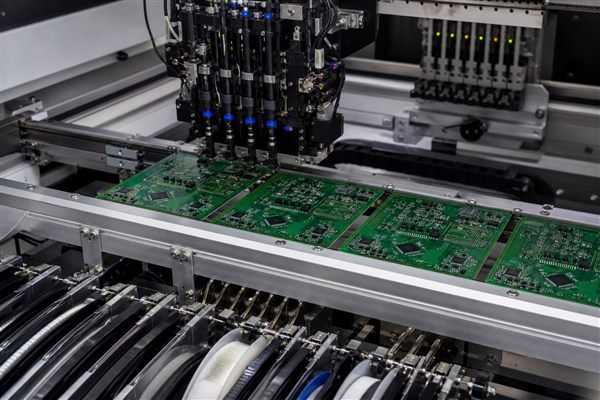
- Release one controlled data package: Confirm the Gerber or ODB++ data, drill files, stackup, fabrication drawing, impedance notes, BOM, centroid data, assembly drawings, polarity markings, firmware requirements, and test specification all identify the same revision.
- Complete fabrication and assembly DFM: Review copper balance, annular rings, drill-to-copper spacing, solder-mask clearances, thermal vias, fine-pitch pads, stencil access, connector mechanics, panelization, tooling, fiducials, and test-point access. Resolve conflicts before material is issued.
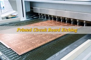
- Fabricate the bare PCB: Process the specified laminate and copper construction through imaging, etching, drilling, plating, solder mask, legend, surface finish, profiling, and final cleaning. Maintain the approved stackup and finished copper requirements for power and return paths.
- Verify the bare boards: Perform electrical continuity and isolation testing against the released netlist. Check finished thickness, hole size, copper-related dimensions, solder-mask registration, surface finish, outline, and controlled-impedance coupons when the drawing requires them.
- Control components and substitutions: Verify manufacturer part numbers, ratings, package types, moisture sensitivity, polarity, date or lot requirements, and storage condition. Do not substitute the controller, power device, sense resistor, reference, protection parts, or laser connector without documented engineering approval.
- Print solder paste consistently: Use a stencil aperture design suited to fine-pitch components, exposed thermal pads, and the required solder volume. Inspect paste coverage and alignment before placement to reduce opens, bridges, voiding, and component float.
- Place and reflow SMT components: Load the verified program and feeders, confirm orientation of polarized and laser-interface parts, and run a profile compatible with the PCB finish and component limits. Control heating and cooling so thermal-pad joints form without damaging temperature-sensitive parts.
- Install connectors and through-hole parts: Use the specified hand-soldering, selective-soldering, or press-fit process. Support mechanically loaded connectors, control solder fill and heat exposure, and verify that the laser-output polarity remains unmistakable after assembly.
- Clean, inspect, and identify the assembly: Remove residues when the process specification requires cleaning, then perform the defined workmanship inspection and any necessary hidden-joint verification. Mark the PCB revision, assembly revision, lot or serial identity, and rework status so every released board can be traced to its materials and process records.
How Should a Laser Diode Driver Board Be Inspected and Tested?
Inspection and testing must verify assembly quality, regulated output, protection behavior, and traceable acceptance results. No single method is sufficient: optical inspection finds workmanship defects, while powered tests confirm current control and fault response.
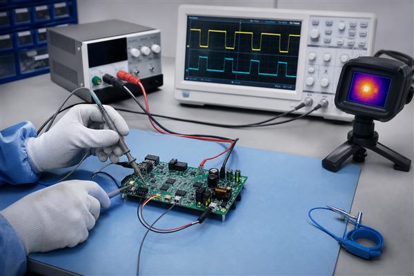
- Verify materials and traceability: Match critical component manufacturer part numbers, ratings, polarity, approved substitutions, PCB revision, assembly revision, and lot information to the production record. Quarantine any unapproved or unidentified deviation before testing.
- Inspect soldering and placement: Use visual inspection and AOI to check missing, shifted, reversed, tombstoned, bridged, or poorly soldered components. Use X-ray when bottom-terminated packages, exposed thermal pads, or hidden joints cannot be judged from the surface.
- Perform unpowered electrical checks: Measure resistance between supply rails and ground, confirm fuse or protection-path continuity, and check for unintended shorts at the laser output. Verify the connector pinout and disabled-state path before applying power.
- Check controlled power-up: Start with a current-limited supply and a specified dummy load. Confirm quiescent current, internal rails, reference voltage, enable logic, interlock state, fault indication, and output behavior while the driver remains disabled.
- Measure regulation performance: Test the commanded output at the required low, nominal, and high operating points. Record current accuracy, stability, ripple or noise where specified, compliance behavior, and channel-to-channel consistency for multi-channel boards.
- Verify dynamic operation: Measure startup, shutdown, enable transitions, modulation response, pulse amplitude, rise and fall behavior, overshoot, ringing, and settling using the approved load, cable, fixture, bandwidth, and probe connection.
- Test protection functions: Exercise the applicable open-load, short-circuit, reverse-polarity, interlock, undervoltage, overtemperature, and emergency-shutdown conditions. Confirm the trip threshold, peak stress, response time, latch state, and permitted recovery sequence.
- Confirm thermal performance: Operate at the specified current, duty cycle, ambient condition, and enclosure or airflow arrangement until the defined stabilization point. Measure power devices, sense resistors, connectors, reference circuitry, and identified PCB hot spots against their acceptance limits.
- Record and control test results: Tie the fixture, software, instrument identification, calibration status, limits, measurements, failures, rework, and retest result to the board lot or serial number. Define whether testing is 100 percent or sample-based and state the sampling rule in the quality plan.
- Define optical and system-level scope separately: Optical-power calibration, beam alignment, laser classification, and finished-system safety verification require the laser, optics, enclosure, and agreed safety procedure. Include these tasks explicitly in the quotation and acceptance specification when the PCBA supplier is expected to support them.
What Files and Specifications Are Required for a Laser Diode Driver Board Quote?
One revision must define the board, assembly, and evidence. Gerber or ODB++ files alone may price a bare PCB, but they do not define component sourcing, assembly workmanship, firmware loading, transient testing, or optical-system responsibilities.
- Fabrication data: Gerber or ODB++, NC drill files, stackup, fabrication drawing, dimensions, tolerances, finish, copper weights, and impedance notes.
- Assembly data: BOM with manufacturer part numbers, centroid file, assembly drawings, polarity notes, approved alternatives, and do-not-fit positions.
- Electrical requirements: input range, current range, compliance voltage, operating mode, modulation limits, polarity, connector pinout, and protection thresholds.
- Test requirements: load model, setup, firmware, instruments or fixture interface, test points, limits, report format, and sample retention.
- Commercial inputs: prototype and production quantities, delivery destination, packaging, traceability, and target schedule.
Send synchronized files with a revision index and identify which document controls when values conflict. This reduces quotation assumptions and gives the PCB/PCBA team enough information to return DFM questions before material procurement.
Why Choose EBest Circuit for Laser Diode Driver Board Manufacturing?
Choose EBest Circuit when the project needs coordinated PCB fabrication, component assembly, inspection, and documented test requirements under one approved manufacturing scope. The customer retains control of the product design and acceptance criteria, while the manufacturing package defines exactly what the supplier must build and verify.
- Coordinate bare-board and assembly reviews: EBest Circuit can review the supplied stackup, fabrication data, BOM, placement files, assembly drawings, polarity notes, and test requirements together. This helps expose conflicts between PCB construction, component footprints, thermal pads, connectors, and test access before production starts.
- Support prototype-to-production continuity: Keep the PCB revision, BOM, approved substitutions, assembly instructions, and inspection criteria aligned as quantities increase. Documented changes reduce the risk that a successful prototype is rebuilt with an uncontrolled material or process difference.
- Protect critical electrical and thermal features: Identify high-current copper, Kelvin-sense connections, switching nodes, controlled returns, thermal vias, exposed pads, and laser-output polarity as controlled features. These requirements can then be carried into DFM, process planning, inspection, and test documentation.
- Define inspection around actual risks: Specify visual inspection, AOI, X-ray, bare-board electrical test, powered functional checks, or fixture-based testing according to the board construction and acceptance plan. The quotation should state which checks are included, their coverage, and the required records.
- Prepare an actionable manufacturing request: For a laser diode driver board quotation, provide the stackup, finished copper, operating current, duty cycle, thermal constraints, critical components, connector pinout, test points, load model, fixture interface, quantities, and acceptance limits.
- Keep responsibility boundaries explicit: State whether firmware loading, functional fixtures, optical-power calibration, beam alignment, laser classification, regulatory certification, and final-system validation are customer-supplied, supplier-supported, or separately quoted. Clear ownership prevents missing work from being discovered after assembly.
FAQs About Laser Diode Driver Boards
Q1: How close should the driver board be to the laser diode?
A1: Keep the high-current connection as short as practical. Remote placement adds cable resistance and inductance, so define cable length, connector type, return path, shielding, and the load used for transient validation.
Q2: Which connector features reduce polarity and service errors?
A2: Use keyed and clearly identified connections. Pin sequencing, locking, touch protection, current rating, mating cycles, strain relief, and a documented de-energized service procedure should match the product risk.
Q3: Can conformal coating be applied to a laser driver PCBA?
A3: Yes, when coating is specified selectively. Keep coating away from connectors, test contacts, adjustment points, optical surfaces, and heat-transfer interfaces unless those parts and the validation plan explicitly permit it.
Q4: How should unassembled boards and components be handled for ESD control?
A4: Define an ESD-controlled handling and packaging plan. Cover receiving, storage, kitting, assembly, test, rework, and shipment, with moisture-sensitive components managed according to their approved handling requirements.
Q5: When should isolation be considered between control and power domains?
A5: Consider isolation when ground potential or fault energy cannot be shared safely. The decision should follow the system architecture, interface voltage, bandwidth, creepage and clearance needs, and the applicable product-safety assessment.
Q6: What should an approved component-substitution record contain?
A6: Record the exact part, reason, review, and affected limits. Include manufacturer part numbers, critical electrical and thermal differences, footprint compatibility, approval authority, applicable revisions, and any required retest.
Q7: How can test points be added without disturbing a fast pulse?
A7: Design the measurement interface with the circuit. Use compact signal-and-ground access, minimize added stubs and loop area, and document the specified probe or fixture so production measurements remain comparable.
Q8: When should burn-in or environmental screening be specified?
A8: Add screening only when the product risk and acceptance plan justify it. Define sample size, temperature, load, duration, monitored variables, failure limits, and disposition before quotation because screening changes equipment time and traceability.
Q9: What packaging protects assembled boards during shipment?
A9: Match packaging to ESD, moisture, shock, and connector risks. Specify protective bags, trays or partitions, desiccant and humidity indication where required, connector caps, labeling, and lot-level traceability.
Q10: Who should control the golden sample and production fixture?
A10: Assign ownership and revision control before repeat orders. The quotation or quality agreement should identify storage, calibration, maintenance, software version, acceptance limits, change approval, and replacement responsibility.
Conclusion
Carry one operating envelope through every production stage. Current regulation, protection, stackup, layout, thermal design, prototype validation, fabrication, assembly, and production testing must remain connected under revision control. This reduces quotation assumptions and prevents a manufacturing handoff from hiding unresolved electrical or optical risks.
If you are sourcing PCB fabrication and PCBA support for a laser diode driver project, send your design files, operating requirements, quantities, and test scope to sales@bestpcbs.com for an engineering review and quotation.