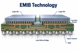
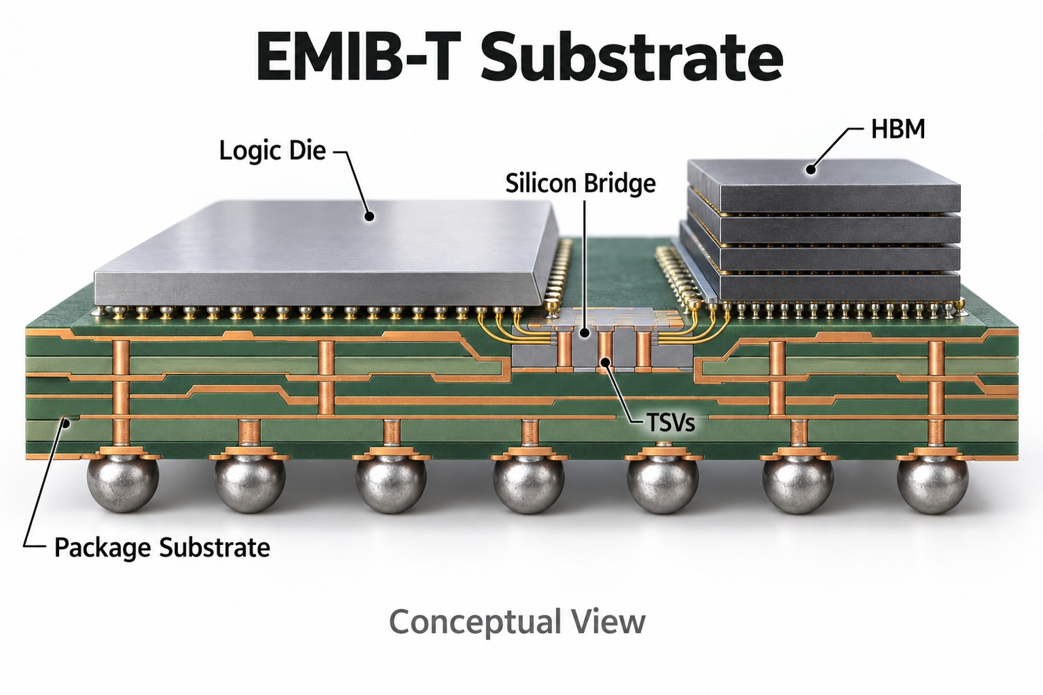
An EMIB-T substrate is a package substrate containing embedded silicon bridges with through-silicon vias (TSVs). The bridges provide dense connections between adjacent chips; their TSVs add a vertical power-delivery route through the silicon. This architecture supports high-bandwidth memory (HBM) and multi-chip computing packages without requiring a full-area silicon interposer. It is a semiconductor packaging structure, not a conventional system PCB. Its manufacturing challenge is integrating small silicon bridges into a much larger substrate while maintaining alignment, electrical continuity and mechanical reliability.
Key Takeaways
- An EMIB-T substrate uses localized silicon bridges embedded inside the package substrate rather than placing the entire multi-die system over one large silicon interposer.
- The defining development from conventional EMIB to EMIB-T is the addition of through-silicon vias (TSVs) in the bridge, enabling vertical connections and more direct power delivery.
- EMIB-T combines fine-pitch lateral die-to-die routing with vertical electrical paths, which is increasingly important for high-power AI accelerators and HBM-based packages.
- Intel has positioned EMIB-T for large AI and HPC packages involving HBM4/HBM4e, UCIe chiplet links, and packages extending well beyond a single reticle.
- EMIB-T and CoWoS-L both use localized silicon for high-density connections, but their package architectures, interposer structures, routing approaches, and assembly flows differ.
- As package dimensions and power rise, warpage, thermal behavior, power integrity, bridge alignment, TSV reliability, and known-good-die management become increasingly important.
What Is an EMIB-T Substrate?
An EMIB-T substrate integrates TSV-equipped silicon bridges into a semiconductor package substrate. EMIB means Embedded Multi-die Interconnect Bridge; EMIB-T is the TSV-enabled evolution of that technology.
Intel EMIB packaging concentrates fine interconnects where neighboring chip edges need them. The surrounding substrate carries broader package routing and mechanical support. This avoids treating every connection as though it needs the same fine-pitch silicon routing.
At EBest Circuit, our work is downstream of this packaging stage. We support system-level boards and PCB assembly, not fabrication of the embedded bridges or EMIB-T substrates.
How Does EMIB-T Work?
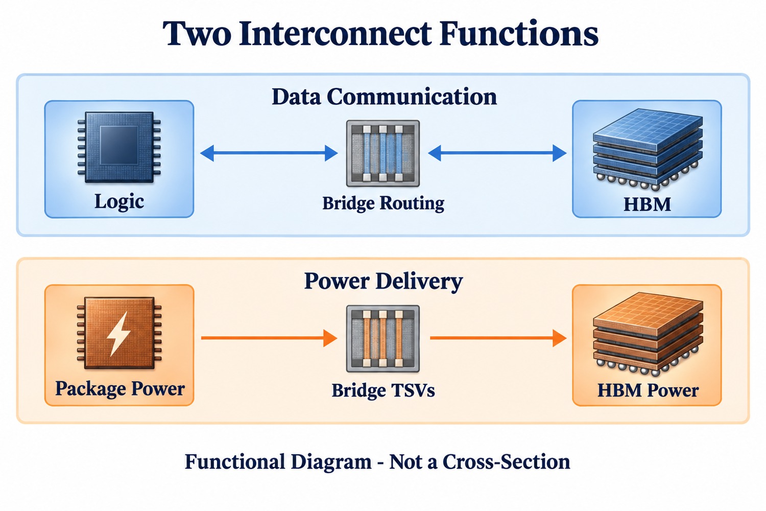
EMIB-T combines short chip-to-chip signal paths with a power route that passes vertically through the bridge. The two functions share an integration region but are not interchangeable electrical nets.
- Data: one die connects through fine-pitch joints to bridge wiring, which reaches the neighboring die.
- Power: package conductors connect through bridge TSVs toward the die power connections.
- System interface: the rest of the package routing connects the assembled device to its external terminals.
The functional diagram separates these paths. It does not represent a production cross-section or a specific pin assignment.
What Is Inside an EMIB-T Package Substrate?
The substrate combines organic dielectric and copper routing with embedded silicon bridges and their vertical connections. The logic dies and HBM sit above this structure; external package connections sit below it.
| Element | Function |
| Organic substrate structure | Mechanical support and package-level routing |
| ABF build-up dielectric and copper | Insulation between conductive routing layers in ABF-based implementations |
| Embedded silicon bridge | Localized high-density interconnect between chip edges |
| Bridge TSVs | Electrical connections through the silicon thickness |
| Fine-pitch bumps | Connections between die pads and bridge-side routing |
| Bonding and dielectric materials | Attachment, insulation and mechanical integration |
| External BGA connections, where specified | Connection from the completed package to the system PCB |
Ajinomoto Build-up Film provides electrical insulation for high-performance package substrates. It should not be confused with the glass-reinforced core that a particular substrate may also contain. Our ABF substrate materials and supply guide explains the wider material and sourcing context. An actual stackup still requires the package supplier’s approved material set.
EMIB vs EMIB-T: Key Differences
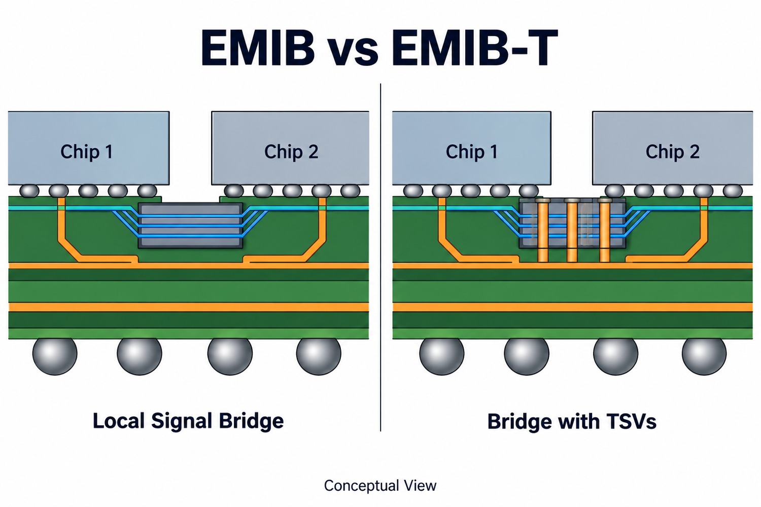
The defining difference is that EMIB-T adds through-silicon connections to the embedded bridge. Conventional EMIB already provides lateral die-to-die interconnects; it does not need bridge TSVs to perform that role.
| Feature | Conventional EMIB | EMIB-T |
| Local silicon bridge | Yes | Yes |
| Bridge TSVs | Not part of the basic architecture | Added to enable vertical connections |
| Bridge-region power access | Supplied through surrounding package routing | Additional direct path through the bridge |
| Integration requirements | Bridge placement and fine-pitch die connections | Those requirements plus TSV and backside connection integration |
Why Does EMIB-T Add TSVs to the Silicon Bridge?
TSVs provide a more direct power route through a region that would otherwise require routing around the bridge. Intel identifies vertical power delivery with low DC and AC noise as a driver for EMIB-T, particularly for HBM.
Intel’s AI and HPC platform brief also describes bridge-integrated MIM capacitors and reduced-impedance vertical power delivery. TSVs provide a conductive path; capacitors provide local charge storage. Neither removes the need to analyze the complete power-distribution network.
Resistance contributes to DC voltage drop, while inductance affects transient voltage when current changes. Short bridge signal routes still require suitable bump geometry, reference paths and decoupling. Electrical benefit therefore depends on the complete package design, not TSV presence alone.
What Is the EMIB-T Process Flow?
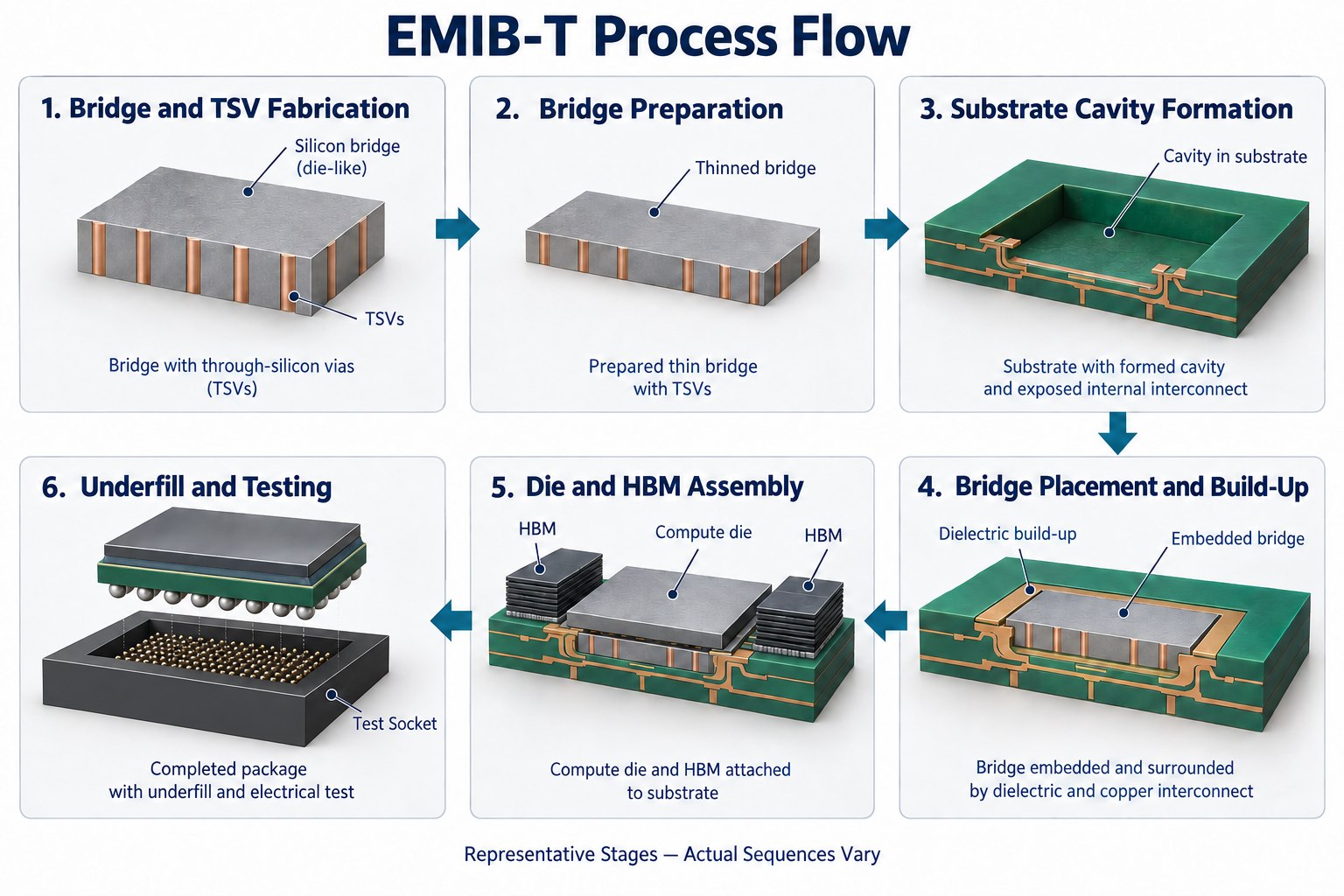
The EMIB-T process flow combines TSV-equipped bridge preparation, embedding, substrate build-up and multi-die assembly. The stages below summarize integration tasks, rather than a fixed Intel manufacturing recipe.
- Prepare the silicon bridge: form fine routing and TSV connections, then prepare the bridge for integration. TSV formation, thinning and backside processing follow the selected bridge process.
- Prepare substrate cavities: create the local spaces and underlying connection structures required by the package layout.
- Place and bond the bridges: control lateral registration, seating height and attachment quality.
- Build dielectric and copper layers: integrate the bridge with surrounding substrate routing and connection pads.
- Assemble logic dies and HBM: connect the die interfaces to the bridge and package substrate using the specified assembly flow.
- Reinforce and test: complete applicable underfill or bonding operations, electrical checks and reliability qualification.
Intel’s EMIB product brief describes cavity embedding, attachment and dielectric/metal build-up. EMIB-T adds vertical bridge integration; exact TSV processing order and acceptance limits depend on the qualified implementation.
Why Is EMIB-T Substrate Manufacturing Difficult?
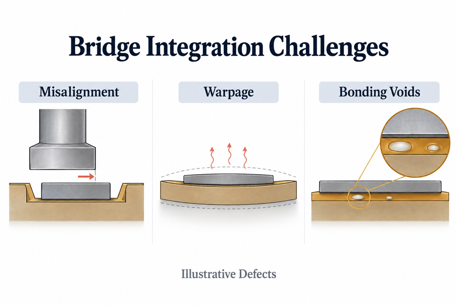
Manufacturing must align a small, rigid silicon insert with multilayer substrate wiring and die contacts through repeated processing steps. The EMIB process flow already requires this registration; EMIB-T adds the bridge’s vertical connections. Placement accuracy at one temperature does not prove alignment after bonding or subsequent thermal cycles.
- Lateral registration: bridge pads must align with the next interconnect level.
- Height control: bridge and substrate surfaces must support consistent connections rather than uneven contact.
- Thermomechanical compatibility: different expansion behavior can produce local stress and displacement.
- Bonding integrity: attachment materials must bond without defects that undermine the structure.
- TSV reliability: evaluate copper continuity and interface stress through the specified thermal-cycling and electrical tests.
- Thermal design: co-design the die layout, thermal interface material and cooling hardware to manage local heat concentration.
- Known-good dies: screen expensive die inputs and use staged electrical checks to limit the cost of late assembly failures.
What Causes EMIB-T Yield Challenges?
Misregistration, nonuniform height and bonding defects can make otherwise usable bridge and substrate components fail after integration. More interfaces also create more opportunities for a defect to interrupt an electrical path.
A September 23, 2026 TrendForce News report, citing supply-chain sources, put EMIB substrate yield at approximately 45%. Its reported targets were 50% in Q4 2026 and 60% in Q1 2027. These are reported substrate-stage figures and future targets, not Intel-published production data or a verified yield for every EMIB-T package.
The September 2026 supply-chain report specifically discussed thermal-expansion mismatch, bridge positioning and bubbles in non-conductive film beneath bridge TSV connections. Those are reported production challenges, not a published defect breakdown across all suppliers.
A useful yield discussion must identify the tested population. Bridge-wafer yield, integrated-substrate yield and final electrical package yield have different denominators. A quoted percentage without its process stage, product complexity and test criteria cannot reliably predict delivered device availability.
EMIB vs CoWoS: What are Differences?
EMIB embeds local silicon bridges in the package substrate; TSMC describes CoWoS as a family of interposer-based technologies. CoWoS-S uses a continuous silicon interposer, whereas CoWoS-L combines an RDL interposer with local silicon interconnects.
| Architecture | High-density interconnect structure |
| EMIB-T | Local TSV-equipped silicon bridges embedded in the package substrate |
| CoWoS-S | Silicon interposer spanning the integrated die arrangement |
| CoWoS-L | RDL-based interposer incorporating local silicon interconnects |
Local bridges reduce the silicon area devoted to interconnection, but add integration demands at each bridge location. A larger silicon interposer supports routing across a wider area; its manufacturing approach is different. Neither description proves that one complete package is always cheaper or has better yield.
For a closer structural comparison, our CoWoS-L explanation distinguishes local silicon interconnects from the surrounding RDL. CoWoS-L is not an all-silicon interposer, and it is not simply another name for EMIB-T.
How Does EMIB-T Support HBM4, HBM4e and UCIe?
EMIB-T supports dense memory and chiplet interfaces by combining short lateral silicon routes with vertical power access through the bridge. AI accelerators and HPC processors need both: more data connections alone do not solve the power demands of the connected dies.
- HBM4/HBM4e: wide logic-to-memory interfaces need dense routing close to the compute die. Bridge TSVs add power paths through that crowded region.
- UCIe: short chiplet links need controlled interconnect geometry and return paths, alongside the power network.
- Large packages: placement and routing must be evaluated together with thermal and mechanical behavior.
In its ECTC 2026 technology update, Intel reported these development results:
- 25 μm first-level interconnect bump pitch.
- 120 × 120 mm package dimensions.
- More than nine reticle areas of compute and memory silicon in one package.
- Signal and power co-optimization supporting 12 Gb/s HBM4e and 64 Gb/s UCIe transmission.
These are technology-development results, not universal specifications for every production package. Separately, Synopsys’ EMIB-T design-flow discussion describes large-design demands including footprints of 120 × 180 mm. That design context should not be combined with Intel’s demonstration dimensions into a single qualified manufacturing range.
Where Is EMIB-T Used in AI and HPC Packaging?
EMIB-T is designed mainly for large AI and HPC packages that integrate multiple compute dies, HBM stacks, and high-speed chiplet interfaces.
Typical applications include:
- AI training accelerators;
- AI inference processors;
- HPC accelerators;
- multi-die GPU or XPU packages;
- chiplet-based CPUs;
- UCIe-based heterogeneous processors;
- multi-HBM compute modules;
- data-center processors.
The package has to move large volumes of data between dies, feed high current to compute silicon, connect several HBM stacks, and control thermal and mechanical stress at the same time.
EMIB-T is particularly relevant where localized high-density silicon routing is needed but using one continuous silicon interposer across the whole package is not the preferred architecture.
Is an EMIB-T Substrate the Same as a PCB?
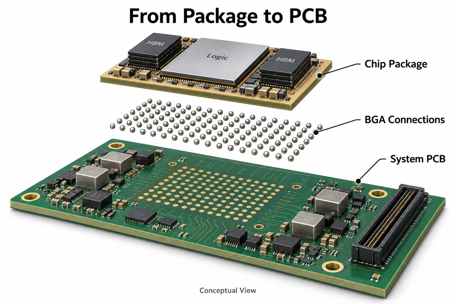
No. The EMIB-T substrate is part of the semiconductor package; the system PCB connects that completed package to the rest of the electronic system.
A TSV passes through silicon. A package-substrate microvia passes through a dielectric layer. A PCB via connects copper layers in a board. They differ in materials, dimensions and manufacturing processes, even though all provide electrical connections between levels.
For a BGA-mounted device, the board land pattern comes from the external ball map and package drawing—not from the pitch of the bridge’s internal microbumps. Using an internal packaging dimension as a PCB footprint dimension would address the wrong interface.
FAQ About EMIB-T Substrates
Is EMIB-T the same as EMIB-M?
No. Intel’s technology brief uses EMIB-M for bridge-integrated metal-insulator-metal capacitors and EMIB-T for the TSV-enabled solution. Later descriptions of EMIB-T also discuss MIM capacitors. TSVs and capacitors perform different functions, so the names should not be treated as interchangeable material grades.
Does EMIB-T require a glass-core substrate?
No. Public Intel descriptions include organic-substrate implementations. EMIB-T identifies the embedded-bridge technology, not a universal core material. A proposed glass-core implementation would require its own approved stackup and reliability evidence; it should not be assumed from the EMIB-T name.
Is EMIB-T the same as Foveros?
No. EMIB-T provides local bridge connections between neighboring dies, while Foveros technologies support other integration arrangements, including vertical die stacking. Intel describes combining the technologies in EMIB 3.5D. A combined package does not make their interconnect structures identical.
Can an existing package move to EMIB-T without redesign?
Not automatically. Die interfaces, bump assignments, power paths and mechanical constraints need to match the chosen packaging flow. Synopsys’ reference-flow announcement includes early bump and TSV planning and multiphysics analysis, illustrating why a technology migration is an engineering project rather than a material substitution.
Can PCB-level X-ray inspection certify the internal silicon bridge?
No. Inspecting board-level solder joints does not qualify buried package interconnects. Package acceptance requires the package supplier’s electrical and reliability evidence. PCB assembly inspection evaluates the board-level work and cannot replace semiconductor-package qualification.
What Does EMIB-T Mean for PCB and PCBA Projects?
For downstream manufacturing, the practical requirement is a released package specification and a board design matched to it. The packaging architecture alone does not set PCB layer count, laminate grade or assembly temperature.
- Footprint and routing: confirm the package drawing, ball map and approved land pattern before PCB design review.
- Power and thermal requirements: use device-level current and cooling specifications to review the board power network and mechanical clearances.
- Assembly plan: check the supplied component’s handling, moisture sensitivity and mounting instructions, together with the agreed inspection and functional-test scope.
At EBest Circuit, we support PCB fabrication, component sourcing and PCBA projects, with suitability confirmed against the actual design. Send the processor package specification, PCB files, BOM, quantities and test requirements to sales@bestpcbs.com for a project-specific review.