An I/O connector is the physical connection that carries signals, data, power, or ground between a PCB and an external cable, device, or system.
A workable choice must satisfy the connector type, PCB mounting, electrical and mechanical limits, environment, mating compatibility, and PCB integration. A part that fits the panel can still fail if its pinout, footprint, cable clearance, or retention does not match the design.
What Is an I/O Connector?
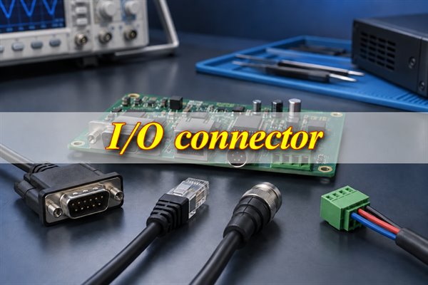
An I/O connector is the physical mating point for signals, data, power, or ground crossing a product boundary. To specify one correctly, separate the connector itself from the port users see and the interface the electronics implement.
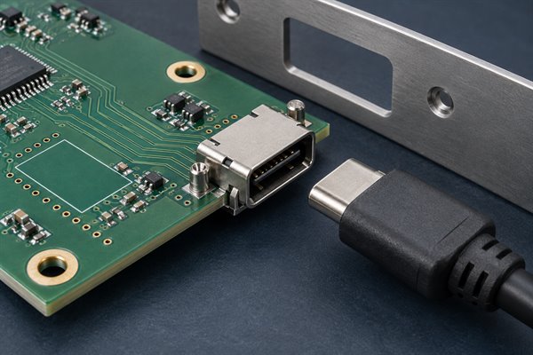
A connector is not the same as a port or an interface. The connector is the physical mating hardware. The port is the accessible connection point on the product. The interface includes the electrical and logical behavior behind that port, such as protocol, voltage levels, timing, pin assignments, grounding, and power roles. For example, a USB-C receptacle does not reveal which USB generation, data rate, power-delivery role, or Alternate Mode the product supports. Selection therefore starts with the implemented interface, then narrows to a compatible physical connector. Only parts that meet both layers are acceptable; a match on shape alone creates a compatibility risk.
How Does an I/O Connector Work?
A mated I/O connection must preserve three things at once: the signal path, the power and ground path, and the mechanical or shield connection. These paths explain most electrical limits and field failures.
- Signal and data path: Contacts carry analog, digital, clock, control, or differential signals. Contact geometry, pair assignment, adjacent returns, and PCB breakout affect noise and data integrity.
- Power and ground path: Power contacts deliver current while ground contacts complete the return path. Contact resistance, loaded-contact count, copper area, cable size, and ambient temperature determine voltage drop and heat.
- Retention and shielding: Latches, screws, shell stakes, and panel hardware carry mating and cable loads. A shield or conductive shell can control EMI and ESD only when its connection to chassis or the chosen reference is short and intentional.
Every connector adds resistance, inductance, capacitance, and geometric discontinuities. Verify channel performance for high-speed links and temperature rise for loaded power contacts in the intended mated assembly; continuity alone does not reveal either limit.
What Are the Main Types of I/O Connectors?
Choose the connector family by the design constraint that leaves the fewest viable alternatives. Screen space, environment, speed, field wiring, and mating life before comparing individual parts.
| Design Need | Options to Consider | Reject When |
| Limited PCB or panel space | Mini I/O, compact rectangular, low-profile, right-angle, or edge-mount designs | The mated plug, latch, overmold, or cable bend exceeds the available volume |
| Water, dust, vibration, or shock | Rugged circular or industrial rectangular connectors with sealing and positive locking | The stated IP or vibration rating does not apply to the fully mated cable assembly |
| High-speed data | Protocol-qualified modular, high-speed pluggable, shielded mini, or differential-pair connectors | Loss, impedance, return-path, cable, or cage data is missing for the target speed |
| Field wiring and maintenance | Pluggable terminal, field-terminable circular, or keyed removable connectors | Wire range, tool access, touch protection, or service labeling is inadequate |
| Frequent mating | High-cycle contacts with positive alignment and mechanical support independent of solder joints | The specified mating life is below the expected service or test-fixture cycle count |
| Dense mixed signal and power | Rectangular multi-position or mixed-contact systems with defined keying | Pin allocation leaves inadequate ground, creepage, current margin, or mis-mating protection |
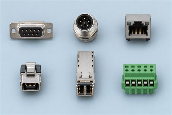
Family names only create a shortlist. Rectangular, mini, and industrial mini connectors can solve similar space problems without sharing a mating interface, so verify the exact series, keying, contact system, and approved mating part.
Where Are I/O Connectors Commonly Used?
Application labels do not choose the connector; the local failure risks do. Compare the electrical load, exposure, cable movement, service access, and data requirement at the connection point.
- Industrial automation: Prioritize positive locking, vibration resistance, serviceable field termination, and an environmental rating that applies in the mated state.
- Servers and networking: Prioritize bandwidth, controlled loss, shielding, port density, cage or module compatibility, and the thermal effect on nearby airflow.
- Robotics and machine vision: Prioritize compact geometry, cable movement, strain relief, vibration resistance, and fast replacement without disturbing adjacent wiring.
- Test and medical equipment: Prioritize mating life, mis-mating prevention, cleanability, touch safety, and replaceable wear components where the application requires them.
- Embedded and computing products: Balance standardized compatibility with connector height, board area, cable exit, user access, and enclosure clearance.
How Are I/O Connectors Mounted and Connected?
Mounting style decides where the connector sits, how the PCB is assembled, and where cable forces go. Compare the six common PCB options against board-edge geometry, routing space, tooling, and required mechanical support.
- SMT: Saves space and suits automated placement, but signal leads should not carry repeated cable force. Use shell tabs, hold-downs, posts, or enclosure support where needed.
- Through-hole: Provides stronger board retention for larger connectors and frequent mating. Check access to both board sides and the required soldering process.
- Press-fit: Suits dense backplanes and high-pin-count interfaces without soldering every contact. Hole diameter, plating, board thickness, insertion force, and tooling are process-critical.
- Right-angle: Places the mating face at the board edge. It saves enclosure height but makes the PCB datum, panel cutout, latch access, and breakout geometry critical.
- Vertical: Supports top-entry mating. Confirm connector height, cable bend, hand clearance, and whether insertion force will flex the PCB.
- Edge or straddle mount: Creates a low-profile board-edge interface. Board thickness, copper geometry, edge tolerance, and connector seating must match the manufacturer’s drawing.
Panel- and cable-mount parts still set the internal harness path, overmold clearance, bend radius, shield termination, and service space around the PCB receptacle.
Which Specifications Matter When Choosing an I/O Connector?
Specifications are useful only when they describe the exact mated and installed configuration. Use the checks below to reject parts that cannot meet the real electrical, mechanical, environmental, or supply condition.
| Specification | Selection Check | Reject When |
| Contact count and pitch | Allocate signals, returns, power, shield, reserved pins, and keying before choosing density | Routing, creepage, test access, or pin allocation cannot be completed cleanly |
| Current | Use loaded-contact derating, temperature rise, contact resistance, cable gauge, and PCB copper | The required current is supported only by a single-contact headline rating |
| Voltage | Check working voltage, transients, clearance, creepage, pollution level, and insulation system | The rating does not cover the actual contact spacing or environment |
| Data rate and impedance | Confirm the protocol, pair geometry, channel loss, return path, cable, and footprint | Performance is claimed only from the connector face or generic bandwidth |
| Mounting and orientation | Fit the complete mated assembly, cable exit, board edge, panel, and assembly process | The receptacle fits but the plug, latch, tool, or cable does not |
| Mating cycles | Include installation, service, qualification, and production-test cycles | Expected use approaches the rating without a replaceable wear strategy |
| IP and environment | Verify sealing state, dust, moisture, vibration, shock, chemicals, and locking method | The rating excludes the selected cable, unmated state, or installation method |
| Temperature | Combine ambient temperature, self-heating, nearby heat sources, and material limits | The connector reaches its limit before the product’s worst-case condition |
| Lifecycle and supply | Check active status, authorized sources, accessories, tooling, lead time, and replacement strategy | The mating ecosystem or required tooling cannot be supported through product life |
Do not approve a connector from a headline rating. Loaded contacts, ambient temperature, cable size, PCB copper, the full channel, and the specified mated or sealed state determine usable performance.
How Do You Choose the Right I/O Connector for Your Application?
Choose the connector by eliminating unsuitable options in a fixed order. Start with what crosses the interface, then screen electrical limits, the mated envelope, mechanical support, environment, and finally the exact mating pair and supply path.
- Specify what must cross the connector. List signals, differential pairs, power rails, currents, returns, grounds, shields, and reserves. Eliminate families that cannot provide the required allocation without unsafe pin sharing or poor return placement.
- Lock the electrical limits. Set voltage, loaded current, allowable drop, protocol, data rate, impedance, isolation, and protection requirements. Eliminate parts whose ratings apply only under easier conditions than the product will see.
- Fit the complete mated assembly. Model the receptacle, plug, latch, overmold, backshell, cable bend, panel, board edge, and service access. Eliminate any option that fits as a bare receptacle but collides when mated.
- Match mounting to the mechanical load. Choose SMT, through-hole, press-fit, vertical, right-angle, or edge mounting based on assembly and force transfer. Eliminate designs that make signal contacts or small solder pads carry cable load.
- Qualify the environment and service pattern. Check sealing, temperature, vibration, shock, chemicals, mating cycles, cleaning, and maintenance. Eliminate options without evidence for the exact installed and mated state.
- Freeze the exact mating pair and PCB implementation. Confirm part numbers, keying, contacts, accessories, pinout, footprint, board datum, lifecycle status, and supply route. Treat any alternate as a design change until all of these items match.
What Should You Consider for High-Speed or Harsh-Environment I/O Connections?
High-speed and harsh-environment requirements fail in different ways and should be screened separately. High-speed selection depends on channel continuity; harsh-environment selection depends on sealing, materials, retention, and installation evidence.
- High-speed path: Verify impedance, return-path continuity, insertion and return loss, crosstalk, pair mapping, cable performance, shielding, and the PCB breakout at the required data rate.
- Harsh environment: Verify the actual mated-state IP or sealing claim, operating temperature, vibration, shock, chemical exposure, corrosion risk, cable retention, and locking method.
Request evidence for the exact connector, cable, accessory, panel, and mounting configuration. For the PCB channel beyond the connector, use the BestPCBS high-speed PCB design guide.
What Should You Check When an I/O Connector Is Mounted on a PCB?
A PCB-mounted connector should be reviewed as one mechanical and electrical interface, not as an isolated footprint. Freeze the part and drawing revision, then check the schematic, land pattern, board edge, enclosure, protection, routing, and assembly access together.
- Footprint accuracy: Match pads, plated holes, support posts, board thickness, paste apertures, and keep-outs to the exact current drawing. Do not reuse a footprint from a similar shell.
- Pin numbering and orientation: Compare the schematic with both the PCB view and mating view. A mirrored pin field can swap power, polarity, or differential pairs even when the footprint looks symmetrical.
- Board-edge and panel datum: Dimension the mating face from controlled PCB and enclosure datums. Include cutout tolerance, gasket compression, screw position, latch travel, plug overmold, and cable bend.
- Anchor tabs and support: Size shell stakes, hold-downs, posts, screws, or brackets for insertion, extraction, vibration, and side load. Do not rely on fine-pitch leads to restrain the connector.
- Solder-joint support: Review thermal balance, paste volume, hole fill, coplanarity, solder wicking, and board flex. Large shell tabs and small signal pins may need different assembly controls.
- Protection placement: Put ESD, surge, termination, or common-mode parts close enough to the entry point to prevent an unprotected trace from carrying the disturbance across the board.
- High-speed breakout: Preserve pair spacing, reference planes, return vias, impedance, polarity, and skew through pads and vias. Avoid plane splits, long stubs, and abrupt geometry changes.
- Shield grounding: Specify whether the shell connects to chassis, circuit ground, or both through a controlled network. Use a short, low-inductance path consistent with the product’s EMC and ESD architecture.
- Assembly and inspection access: Reserve space for placement nozzles, selective soldering or press-fit tooling, cleaning, AOI or X-ray where applicable, rework, fasteners, cable insertion, and latch release.
Trace the complete path from the cable to protected logic. The BestPCBS interface board guide covers the wider entry-path review.
What Common I/O Connector Problems Should You Avoid?
A connector risk is actionable only when the error, consequence, and verification check are all known. The pairs below show what should stop production release.
- Wrong footprint causes an unassemblable board: Pins, posts, or shell tabs miss their lands or holes. Overlay the current manufacturer pattern on the PCB footprint before release.
- A mirrored pinout misroutes power or signals: The board may power the wrong contact or reverse a differential pair. Cross-check PCB view, mating view, cable drawing, and test fixture.
- Weak shell support cracks solder or lifts pads: Cable force reaches fine leads and pads. Verify the load path through anchors, panel hardware, and enclosure support.
- An incorrect board-edge datum prevents mating: The plug hits the panel, misses the opening, or cannot latch. Inspect a tolerance-stack drawing and a fully mated mechanical model.
- Insufficient current margin creates heat and voltage drop: Adjacent loaded contacts run hotter than the headline rating suggests. Review derating and measure the complete power path when risk requires it.
- A poor return path causes data errors or excess emissions: Plane gaps, missing return vias, or long stubs disturb the channel. Review the breakout and reference transition with the intended cable.
- An incorrect shield connection weakens ESD or EMI control: A long shell trace adds inductance or injects disturbance into circuit ground. Verify the chassis and ground strategy at the entry point.
- An incompatible mate damages contacts or prevents latching: Similar appearance hides different keys or contact systems. Approve the exact manufacturer mating pair and accessories.
- Poor inspection access lets assembly defects escape: Solder joints, press-fit pins, or shell tabs cannot be evaluated. Specify AOI, visual, X-ray, electrical, or mechanical checks before production.
What Should You Verify Before Finalizing an I/O Connector?
Before release, confirm that the exact connector can be purchased, assembled, mated, inspected, and supported without reopening the design. Hold production if any item below remains unverified.
- Exact part number: Receptacle, contacts, keys, seals, shell options, accessories, and drawing revision are frozen.
- Mating part: The approved plug, cable, backshell, latch, and keying have been checked as a complete pair.
- Pinout: Signal direction, power, ground, shield, polarity, reserves, and no-connects match the schematic and cable drawing.
- Footprint: Pads, holes, posts, board thickness, keep-outs, paste, and support features match the exact drawing.
- Board-edge position: The mating datum, panel cutout, fasteners, gasket, latch, and cable clearances pass the tolerance review.
- Assembly method: Packaging, placement, soldering or press-fit tooling, cleaning, handling, and rework are defined.
- Inspection method: The plan identifies how solder joints, pin seating, orientation, continuity, retention, and required functional performance will be checked.
- Lifecycle: Supply status, authorized sources, accessories, tooling, expected availability, and qualified-alternate policy are documented.
FAQs About I/O Connectors
Substitution, grounding, protection, wear, and qualification can still change the final connector decision. Confirm each answer against the exact part drawings and product requirements.
Q1. What is the difference between an I/O connector and a board-to-board connector?
A1. An I/O connector normally crosses the product boundary, while a board-to-board connector joins PCBs inside the assembly. The categories can overlap, but external I/O usually needs more attention to user access, cable load, ESD, shielding, panel alignment, and environmental exposure.
Q2. Is SMT or through-hole mounting better for frequent mating?
A2. Through-hole or separately anchored designs usually tolerate repeated external force more easily. SMT can still work when shell stakes, hold-downs, panel support, and the enclosure carry the load instead of the signal pads.
Q3. Should the connector shell connect to chassis ground?
A3. Often, but the correct connection depends on the EMC, ESD, safety, and grounding architecture. A conductive shell is usually most effective through a short, low-inductance path near the entry point. Do not route it through a long PCB trace by habit.
Q4. How do I confirm the correct mating connector?
A4. Use the manufacturer’s approved mating-part table and both product drawings. Match the series, contact system, keying, housing size, orientation, sealing parts, cable range, latch, and accessories. Contact count or appearance alone is not reliable.
Q5. Can I replace an I/O connector with a compatible part from another brand?
A5. Only after full qualification. A claimed equivalent must match the mating standard, pinout, footprint, board datum, keying, ratings, materials, cable system, environmental evidence, assembly process, and lifecycle needs. Similar dimensions do not prove interchangeability.
Q6. What is the most common PCB footprint mistake for an I/O connector?
A6. Mirroring the contact field by confusing the mating view with the PCB view is one of the most damaging errors. Support-post and shell-tab locations are also frequently missed. Overlay the exact current drawing and verify pin 1 from both sides.
Q7. Does an external I/O connector need ESD protection?
A7. Many user-accessible or cable-exposed interfaces need an ESD path, but the device and topology depend on the interface. When protection is required, place it near the connector and keep the discharge path short so the surge does not travel across unprotected circuitry.
Q8. Why can the usable current be lower than the connector’s advertised rating?
A8. The headline value may apply to one contact under a specified test condition. Multiple adjacent loaded contacts, higher ambient temperature, smaller cable conductors, limited PCB copper, or a closed enclosure can raise temperature and reduce usable current.
Q9. Should a production test fixture mate through the product’s I/O connector?
A9. Only when the connector’s mating life and test strategy allow it. Repeated test cycles can consume service life or contaminate contacts. A replaceable fixture-side cable, sacrificial adapter, or dedicated test interface may reduce wear.
Q10. Should the connector and cable assembly be qualified together?
A10. Yes, whenever cable construction affects current, signal integrity, sealing, strain relief, or EMC. Test the intended plug, cable, backshell, termination, and PCB receptacle as the actual channel rather than approving each item in isolation.
Conclusion
Select an I/O connector from the interface requirements and likely failure modes, then verify the complete mating pair on the PCB and in the enclosure. Electrical ratings, footprint, board-edge position, retention, protection, routing, assembly, inspection, and lifecycle must agree before production.
If you are sourcing an I/O connector for a PCB or PCBA project, send the exact part number or candidate series, mating-part requirements, quantity, target delivery date, and acceptable alternatives to sales@bestpcbs.com. EBest Circuit can review the component sourcing request with your PCB or PCBA files and return a quotation or identify details that still need confirmation.