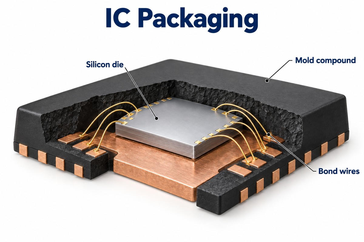
IC packaging turns a fragile semiconductor die into a component that can be handled, electrically connected and mounted in an electronic product. The package provides external terminals, protects the die and creates paths for heat to leave it. It is the chip’s physical enclosure and interconnect structure—not its shipping tray or moisture-barrier bag.
A molded QFN, a wire-bonded BGA and a flip-chip processor package achieve these tasks differently. Understanding what is inside each structure helps explain its electrical behavior, thermal requirements and limits during PCB assembly.
At EBest Circuit, we support the board-level stage through our PCB assembly services, including component sourcing, incoming inspection, assembly and project-defined testing. Our engineering support connects package selection with PCB fabrication and assembly requirements; semiconductor die packaging is a separate manufacturing process.
Key Takeaways
- IC packaging protects a semiconductor die, provides external electrical connections and creates heat-transfer paths. It is different from a shipping tray or moisture-barrier bag.
- Package names describe different structural features. BGA identifies the external ball array; flip chip identifies the internal die connection. A BGA is not necessarily flip chip.
- Wire bonding uses fine wires from a face-up die; flip chip uses bumps beneath a face-down die. Connection density, parasitics and mechanical requirements influence the choice.
- Common materials include copper leadframes, epoxy molding compounds and organic routing substrates. Not every package contains a multilayer substrate.
- Packaging combines die attachment, electrical interconnection, protection and testing. Multi-die structures add integration density but also complicate thermal management and test access.
- An exposed-pad QFN transfers heat into PCB copper through its die paddle and solder joint. The pad’s electrical assignment and board layout must follow the device documentation.
- Board assembly needs package-specific footprint, stencil and inspection decisions. SPI checks printed paste, AOI checks visible features, and X-ray examines hidden solder connections; electrical testing checks operation.
- Moisture handling and reflow limits are component-specific. Use the exact part’s moisture sensitivity label, package drawing and assembly instructions. EBest Circuit supports PCB fabrication and PCBA, not semiconductor die packaging.
What Is Inside an IC Package?
A typical molded IC package contains a semiconductor die, a die attachment layer, electrical interconnects, a leadframe or package substrate, and protective molding compound.
- Die: the piece of semiconductor containing the active circuit.
- Die attachment: an adhesive, solder or other qualified bonding material that secures the die to its support. The required electrical and thermal properties depend on the device.
- Internal interconnects: wires, bumps or other structures that connect die pads to the package routing.
- Support and routing: a metal leadframe or multilayer substrate carries connections toward the external terminals.
- Protection: molding compound, a lid or another enclosure protects vulnerable structures.
A leadframe package does not need the same internal routing stack as a substrate-based BGA. A package substrate, in turn, is not the motherboard: it redistributes fine die connections to the package’s external connections. Our explanation of IC substrates and how they differ from PCBs covers that distinction.
IC Packaging Types
IC packaging types can be grouped by external terminal format, internal connection method or integration architecture. These classifications overlap: “BGA” describes the external ball array, while “flip chip” describes how the die connects inside the package.
| Classification | Examples | What It Describes |
| External terminals | DIP, QFP, QFN, BGA | How the finished component connects to the board |
| Die connection | Wire bonding, flip chip | How die pads connect to package conductors |
| Integration architecture | Single-die package, SiP, stacked-die package | How multiple functions or dies are arranged |
For example, a QFN commonly uses a copper leadframe with bottom-side lands and may include an exposed thermal pad. A flip-chip BGA instead connects the die through bumps to a routing substrate, with a separate ball array underneath for board attachment. For footprint and assembly comparisons, see our IC package types guide.
Which IC Packaging Materials Are Used?
Common IC packaging materials include copper alloys for leadframes, epoxy molding compounds for encapsulation, organic laminates for substrates, and metals such as copper, gold or aluminum for bond wires.
| Material | Package Location | Primary Function |
| Copper alloy | Leadframe and die paddle | Electrical conduction and mechanical support |
| Filled epoxy molding compound | Molded body | Encapsulation and electrical insulation |
| Organic laminate and copper routing | Package substrate | Signal and power redistribution |
| Bond-wire metals | Die-to-terminal connections | Electrical interconnection |
| Underfill resin | Gap beneath a bumped die | Mechanical reinforcement of interconnects |
| Ceramic and metal lids | Selected cavity or hermetic packages | Structural support and environmental protection |
Epoxy molding compound is a common IC packaging plastic material, but it is an engineered composite rather than ordinary unfilled plastic. Resin chemistry and fillers affect flow, expansion, moisture behavior and reliability. Sumitomo Bakelite’s EME encapsulants, for example, are specifically developed for semiconductor packaging.
Materials must work as a system. A low-expansion encapsulant alone cannot eliminate stress if its adhesion, curing behavior or compatibility with the die and substrate is unsuitable. The package manufacturer qualifies the complete material combination, not just one favorable property.
How Do Wire Bonding and Flip Chip Differ?
Wire bonding connects a face-up die to package terminals with fine wires; flip chip connects a face-down die through bumps directly to matching pads on a substrate or other receiving structure.
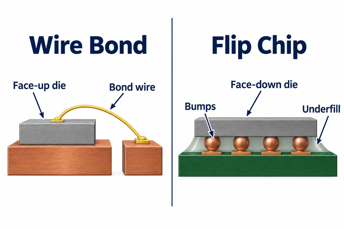
Wire bonding accommodates many established analog, power-management and logic packages. Its wire loops introduce electrical parasitics, and the bond-pad arrangement and loop geometry constrain the layout. Wire material and bonding settings must be compatible with the die metallization.
Flip chip supports connections across the die surface rather than only along an accessible perimeter. Its shorter interconnects can reduce inductance and support dense signal and power connections.
The trade-off is additional control of bump formation, alignment, substrate routing and mechanical stress. Underfill is used in many flip-chip structures to reinforce the connection region; the exact material and application sequence depend on the package. Neither method is universally better for every IC.
IC Packaging Process
The IC packaging process typically prepares and separates wafer dies, attaches each die, forms electrical connections, protects the assembly, and tests the finished devices. A molded wire-bonded leadframe package follows the example below.
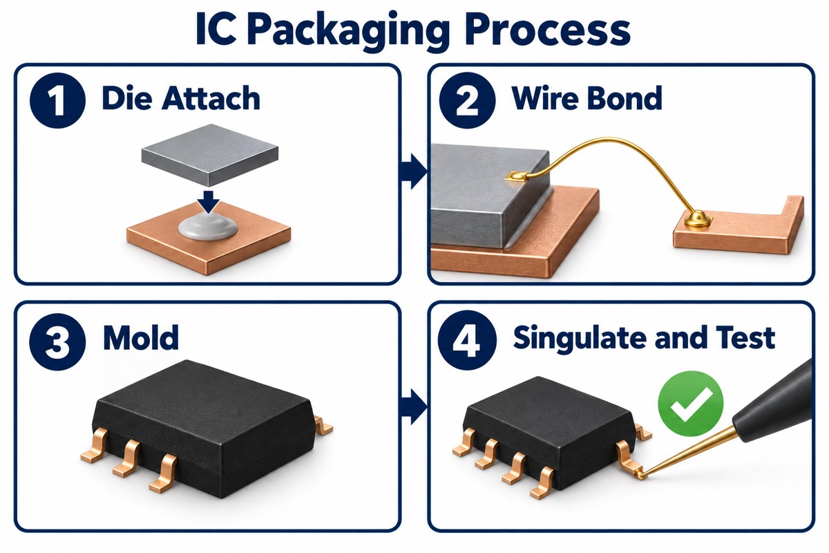
- Prepare the dies: wafer-level inspection and electrical probing identify die performance before packaging; wafer preparation and dicing separate individual dies.
- Attach the die: place it on the designated paddle or support using the qualified attachment process.
- Form interconnects: bond wires between die pads and separate leadframe terminals.
- Encapsulate: mold the body around the die and wires, then complete the required cure and finishing operations.
- Separate and finish: singulate individual packages; terminal finishing or lead forming applies where the package design requires it.
- Test and pack: electrically test, inspect, mark and prepare accepted devices for shipment.
The illustrations simplify these stages and are not tooling drawings. Flip-chip, cavity and wafer-level packages use different sequences; a ceramic cavity package, for instance, may require lid sealing rather than plastic molding. Process order is defined by the particular package flow.
Why Are Multiple Dies Combined in One Package?
Multiple dies are combined to integrate functions, shorten communication paths or place different semiconductor technologies in one component or module.
A system-in-package (SiP) may combine logic, memory, radio-frequency devices and passive components. It can use several interconnect and assembly technologies rather than a single universal construction.
- Side-by-side integration: dies occupy neighboring locations on a common routing structure.
- Stacked-die integration: dies sit above one another; their connections may use wires or other vertical interconnect structures.
- Interposer-based integration: an additional fine-routing structure connects dies before signals reach the package substrate.
These arrangements increase the importance of thermal interaction, interconnect yield and testing access. A failed die or connection can affect the completed assembly. Our CoWoS-S packaging article examines one interposer-based architecture in more detail.
How Does Heat Leave an IC Package?
Heat leaves an IC through paths into the PCB, the package surface and any attached cooling hardware. In an exposed-pad QFN, an important path runs from the die through its attachment and paddle, through solder, and into PCB copper.
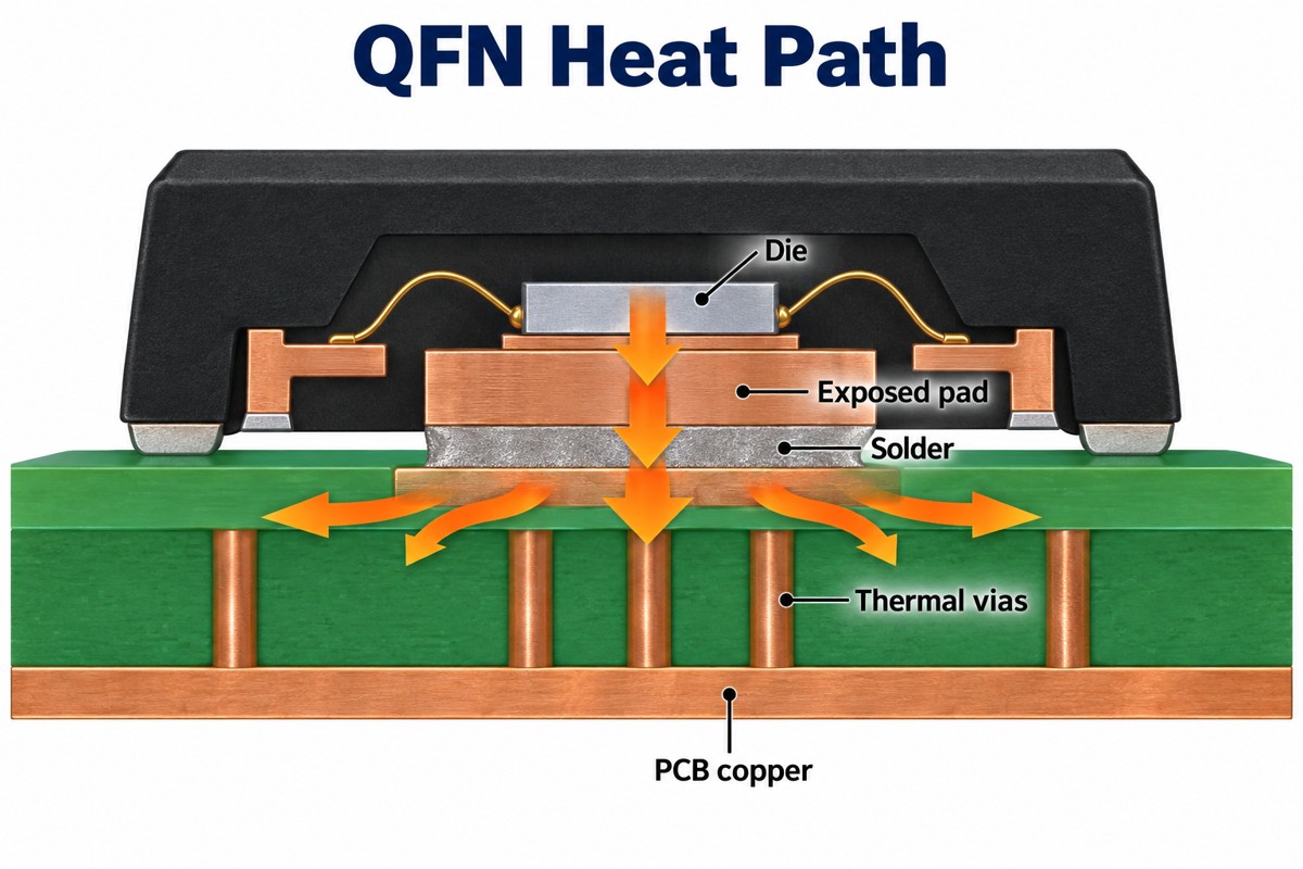
The exposed pad needs the land pattern, solder connection and copper arrangement specified for that component. Thermal vias can connect the top land to additional copper layers. Their dimensions, filling or tenting treatment and stencil layout must also account for solder loss into holes and assembly quality.
Not every exposed pad is an interchangeable ground connection. Its electrical assignment comes from the device datasheet. Likewise, a thermal resistance value is meaningful only with its stated board and test conditions; it is not a fixed prediction of temperature on every PCB.
For a lidded processor package, heat transfer through a thermal interface material and heat spreader may be central to the cooling design. That is a different assembly from the QFN example and should not inherit its thermal-pad rules.
How Are IC Packages Tested?
IC packages undergo electrical testing to confirm device operation, while inspection and reliability qualification address assembly defects and resistance to specified stresses.
- Electrical testing: checks functions and relevant parameters after assembly, using the device’s test program.
- Visual and dimensional inspection: checks body condition, markings, terminal geometry and other specified characteristics.
- Internal inspection: X-ray or acoustic methods may investigate hidden connections, voids or delamination, according to the inspection plan.
- Reliability qualification: evaluates defined stresses such as temperature cycling or humidity exposure on the applicable qualification samples.
These checks answer different questions. Passing an electrical test does not prove that a package has no internal structural defect, and a clear X-ray image does not establish full device functionality. Burn-in and system-level testing are product-dependent, not mandatory stages for every IC.
What Can Damage an IC Package During PCB Assembly?
Moisture exposure followed by reflow, excessive temperature, electrostatic discharge and mechanical stress can damage an IC package or its internal connections.
Absorbed moisture is especially important for moisture-sensitive surface-mount components: rapid heating can generate internal pressure and contribute to cracking or delamination. The moisture sensitivity level, permitted floor life and peak package-body temperature must be taken from the component’s label and applicable handling instructions.
- Before placement: confirm the exact ordering code, package drawing, moisture status and storage history.
- During reflow: use a validated profile compatible with the component, solder paste and board; oven settings alone do not show the component’s actual temperature.
- During handling and rework: control ESD, avoid excessive board bending, and follow the specified limits on heating and mechanical loading.
Baking is not a universal remedy to apply at an arbitrary temperature. Follow the approved recovery procedure when floor life or storage conditions have been exceeded.
What Should Be Checked Before Mounting an IC Package?
Check the exact package drawing, PCB land pattern, stencil apertures, orientation and inspection plan before releasing an IC for board assembly. A package-family name or pin count alone is not enough to approve the footprint.
- Footprint: compare terminal pitch, pad dimensions, exposed-pad geometry and pin-1 location with the manufacturer’s drawing. A mismatch can produce open joints or incorrect connections even when the body fits.
- Paste printing: evaluate stencil thickness and aperture geometry together. For a rectangular aperture, area ratio is L × W / [2t(L + W)], where t is stencil thickness. Reducing thickness increases this ratio but reduces theoretical paste volume; neither choice should be made from pitch alone.
- Exposed pads: review aperture segmentation and thermal-via treatment to limit excess paste and solder loss into open vias. Do not apply one void-percentage limit to every QFN or power device.
- Inspection: use SPI to evaluate paste height, area and volume before placement. After reflow, use AOI for accessible joints and orientation, and X-ray for hidden BGA or QFN connections. Follow with the agreed electrical or functional tests.
Our SMT stencil service supports the paste-printing stage. Send the package drawing with the PCB and assembly files so aperture and thickness choices can be reviewed together, rather than copied from a different component.
At EBest Circuit, our PCBA process includes SPI, AOI and X-ray inspection. The project’s component geometry and acceptance requirements determine the inspection plan; an X-ray image alone does not prove that a populated board functions correctly.
FAQ About IC Packaging
Is IC packaging the same as PCB assembly?
No. IC packaging builds the component around semiconductor dies. PCB assembly mounts packaged components and other parts onto a circuit board.
Does every IC package contain a substrate?
No. Many molded packages use a metal leadframe instead of a multilayer organic package substrate.
Are all BGA packages flip chip?
No. BGA describes the external solder-ball array. The die inside can use wire bonding, flip chip or another qualified interconnect arrangement.
Are plastic IC packages waterproof?
Ordinary molded plastic packages should not be treated as hermetic enclosures. Environmental suitability depends on the complete package qualification and the product’s protection measures.
Does a 3D package always use TSVs?
No. Dies can be stacked and connected with bond wires. Through-silicon vias are one possible vertical interconnect technology, not a requirement for every stacked-die package.
How Can EBest Circuit Support Your PCB Assembly?
A well-chosen IC package still needs a compatible footprint, soldering process and inspection plan. At EBest Circuit, we bring PCB fabrication, component sourcing and assembly support together so these requirements can be reviewed before your build.
Send your BOM with exact manufacturer part numbers, Gerber files, assembly drawings, quantities and test requirements to sales@bestpcbs.com. We can review your project’s PCB and assembly requirements, identify missing package information, and discuss the next steps for a quotation.