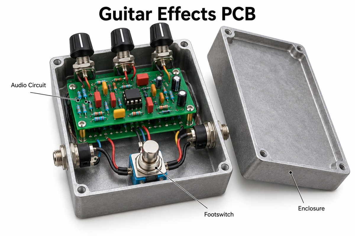
A guitar effects pcb is the printed circuit board inside a guitar pedal that connects its audio-processing components, power circuit and control interfaces. It may implement overdrive, fuzz, filtering, delay or another effect. A dependable board needs more than a correct schematic: input routing, return-current paths, supply filtering and enclosure fit determine whether the finished pedal is quiet, stable and practical to assemble.
At EBest Circuit, we support custom PCB fabrication and PCB assembly from customer-approved designs. For effects projects, we review footprints, polarity markings, control alignment and test access before manufacturing. Circuit ownership and permission to use a design remain separate from the fabrication process.
Key Takeaways
- A pedal PCB carries the audio circuit; a pedalboard holds complete pedals and is a different product.
- Place the input, gain or processing stages and output in signal-flow order, with noisy power and switching nodes kept away from sensitive inputs.
- A 9 V supply does not mean every op amp can handle every signal on that rail. Verify input common-mode range, output swing and biasing.
- Two-layer FR-4 is a practical starting point for many analog pedals; digital effects may need more routing and power-plane resources.
- Through-hole, SMT and mixed assemblies can all work. Component values, packages and circuit behavior matter more than assembly style alone.
- Verify the PCB in its real enclosure, then test DC conditions, audio response, bypass operation and noise.
What Does a Guitar Effects PCB Do?
The PCB connects components that change a guitar signal’s level, frequency response, waveform or timing, while distributing power and carrying control connections.
| Effect | Circuit function | Layout priority |
| Boost | Raises signal level | Input loading and output headroom |
| Overdrive or distortion | Amplifies and clips the waveform | Feedback-loop length and input/output separation |
| Fuzz | Uses nonlinear gain stages | Transistor bias and leakage-sensitive nodes |
| EQ or filter | Changes frequency response | RC values and control wiring |
| Delay or modulation | Processes a time-varying or delayed signal | Clock coupling, power filtering and mixed-signal returns |
A PCB sold as a bare board contains no assembled components unless explicitly stated. A kit may add parts, while a PCBA is a populated circuit board. None of these terms automatically includes an enclosure, firmware or final audio testing.
Guitar Pedal PCB Schematics
Guitar pedal PCB schematics define the electrical connections, component values, bias network and switching arrangement that the layout must preserve. They do not define the enclosure geometry or every manufacturing detail.
Before placing parts, confirm:
- Input and output impedance targets and the expected signal amplitude.
- Supply voltage, connector polarity and reverse-polarity protection.
- Op-amp or transistor pin assignments for the exact package.
- Ground, midrail reference and any negative supply as distinct nets.
- Potentiometer values, tapers and terminal numbering.
- Bypass switching and LED control connections.
For example, a non-inverting stage with a 100 kΩ feedback resistor and 10 kΩ resistor to a low-impedance reference has an ideal small-signal gain of 11 before frequency shaping or clipping is considered. This arithmetic helps check the schematic; it is not a complete overdrive design.
Guitar Effects PCB Layouts
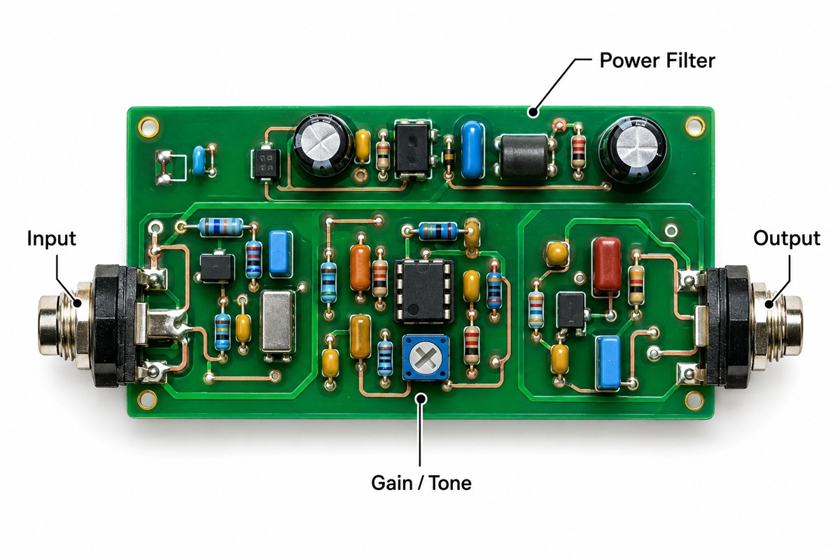
Good guitar effects PCB layouts follow the audio path from input to output and keep high-gain feedback, clock signals and switching currents away from the input. Guitar pedal PCB design begins with placement that makes the quiet path short before routing starts.
- Place the input buffer or first gain device close to the input connection.
- Keep op-amp feedback components beside the relevant pins.
- Separate the final high-level output from the low-level input to reduce unintended feedback.
- Place local decoupling close to each IC supply connection.
- Keep LED, relay and digital return currents out of sensitive analog reference paths.
A continuous ground reference is often easier to control than arbitrary ground splits. Do not route a sensitive signal across a gap in its return plane. Where multiple supply or signal domains exist, plan their current paths rather than relying on labels such as “analog ground” to solve coupling.
How Should a 9 V Pedal Supply Be Designed?
A 9 V pedal supply needs the correct connector polarity, protection, filtering and a bias reference compatible with the audio circuit. Many pedals use center-negative DC power, but the actual product specification must control the design.
For a single-supply analog circuit, a nominal 4.5 V reference may center the audio signal between ground and 9 V. That reference is not chassis ground. Its impedance and loading matter: shared bias movement can modulate multiple gain stages.
Check the exact amplifier variant. Texas Instruments lists a 7 V minimum total supply for the conventional TL072, while the TL072H has a different 4.5–40 V supply range. Similar names do not guarantee identical common-mode limits or output swing. A part operating on 9 V can still distort unintentionally if its inputs or outputs approach their limits.
A 100 nF ceramic capacitor near an IC supply is a common local-decoupling starting point, with bulk capacitance selected for the supply path. Confirm stability and transient behavior using the chosen device’s data sheet; do not copy capacitor values blindly.
Which PCB Construction Fits an Effects Pedal?
A two-layer FR-4 PCB is sufficient for many compact analog effects, while DSP pedals with dense digital routing may benefit from four or more layers. Layer count should follow routing, return-path and power-distribution needs.
| Design item | Example starting specification |
| Analog pedal construction | 2-layer FR-4 |
| Finished thickness | 1.6 mm, subject to mechanical fit |
| Copper | 1 oz nominal, subject to current and fabrication requirements |
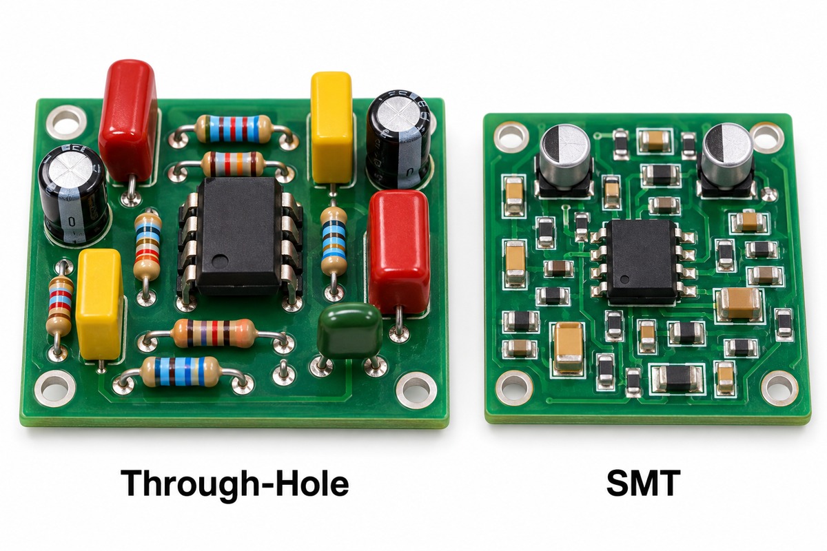
| Through-hole IC example | 8-pin DIP, typically 2.54 mm lead pitch |
| Surface-mount IC example | SOIC-8, typically 1.27 mm lead pitch |
| Audio connector | 6.35 mm jack type selected to match enclosure and footprint |
These are design examples, not a fixed recipe or a list of manufacturing limits. Check the exact component drawing. Different jack bodies, potentiometer heights and switch footprints can make two electrically identical boards mechanically incompatible.
Should You Use Through-Hole or SMT Assembly?
Through-hole parts are convenient for hand-built prototypes and modification; SMT reduces board area and supports automated placement. Mixed assembly often suits pedals that combine small audio electronics with large controls and connectors.
Neither method inherently produces a better tone. Compare the actual resistor tolerance, capacitor behavior, semiconductor characteristics and parasitics. A substitution that preserves a resistance value but changes a potentiometer taper or transistor pinout can still change the product.
For assembly release, specify manufacturer part numbers and approved alternatives. Mark electrolytic polarity, diode orientation and IC pin 1 clearly. Keep component bodies and solder joints away from mounting hardware and enclosure contact areas.
What Mechanical Checks Prevent Enclosure Problems?
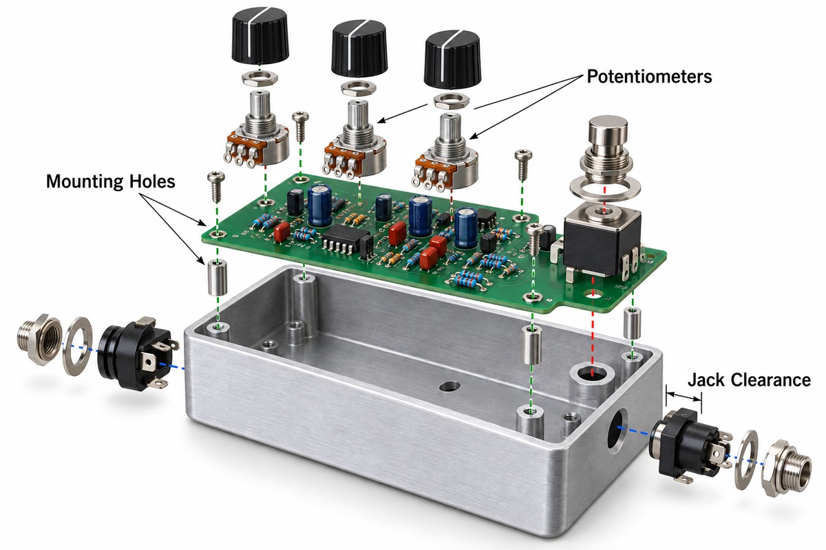
Check the assembled board, control shafts, jacks, footswitch and lid together in a mechanical model or physical fit trial. The bare PCB outline alone cannot prove that a pedal will close without interference.
- Match mounting-hole positions to the actual enclosure drawing.
- Check component height against the lid and base, including tolerances.
- Allow jack plugs, switch terminals and solder joints their full clearance.
- Verify potentiometer shaft length, body height and knob seating.
- Support heavy controls so repeated foot operation does not load small solder joints.
Plan insulation where the underside of the board can approach the metal enclosure. Connector shields and chassis connections should follow the grounding design, not accidental contact through a mounting screw.
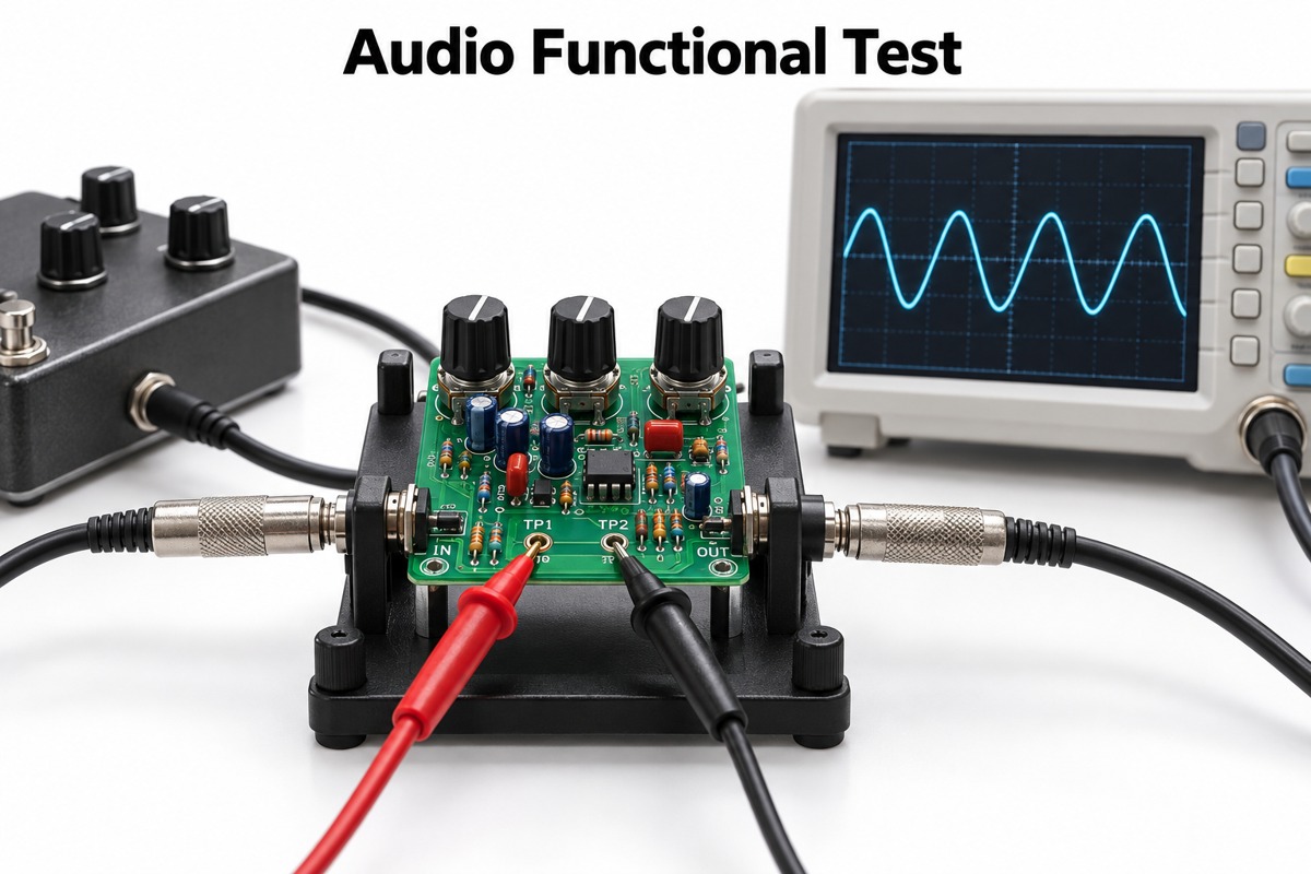
How Should a Guitar Effects PCB Be Tested?
Test supply current and DC bias first, then measure the audio path, controls, bypass and noise under defined input and output conditions. A continuity check alone cannot confirm an effects pedal’s sound or stability.
- Unpowered checks: inspect orientation, solder bridges, connector wiring and supply resistance.
- Current-limited power-up: compare current consumption and bias voltages with the design targets.
- Signal tracing: inject a known signal, such as a 1 kHz sine wave, and follow it through each stage.
- Functional sweep: verify gain, tone controls, clipping onset or delay behavior over the intended settings.
- Noise and switching: measure with a defined source termination, bandwidth and gain setting; check bypass pops and power-on behavior.
- Enclosed test: repeat the relevant checks in the final metal enclosure with the intended supply and cables.
Use a low input amplitude when measuring clean gain, then increase it deliberately to assess clipping. Record test levels and loading so the next batch can be compared with the approved reference unit. There is no universal pass/fail noise number for every pedal.
Why Does a Pedal PCB Hum, Oscillate or Pop?
Hum usually points toward supply or grounding coupling; oscillation often comes from unintended feedback or unstable stages; switching pops can result from DC differences and charge redistribution. Diagnose the symptom before changing parts.
| Symptom | First checks |
| Hum or buzz | Supply ripple, shield connection, loop area, input termination |
| High-pitched whine | Clock or charge-pump coupling into the audio path |
| Oscillation at high gain | Input/output proximity, feedback layout, capacitive loading |
| Pop during bypass | DC at switch contacts, coupling-capacitor charging, switching sequence |
| No audio | Power polarity, IC orientation, jack wiring, switch continuity |
Use an oscilloscope where needed: an oscillating stage may sound weak or harsh rather than produce an obvious audible whistle. Compare one section at a time with the schematic and reference board.
FAQ About Guitar Effects PCB
Can a DIY guitar pedal PCB become a production product?
Yes, after the circuit rights, mechanical fit, BOM, manufacturing data and acceptance tests are resolved. A successful hand-built prototype does not by itself establish repeatability across substituted parts and production batches.
Does a gold finish improve pedal tone?
A surface finish should be selected for solderability, storage and any contact requirement. A claim that a gold PCB finish inherently improves the audio tone is not a substitute for measured circuit performance.
Does every pedal need a four-layer board?
No. Many analog pedals work well on two layers. More layers can help dense DSP layouts and return-path planning, but they do not correct a poor schematic or unsuitable power circuit.
Can one PCB support several effect versions?
Yes, with controlled option parts, jumpers or alternate population. Each version needs an identified BOM and a matching test configuration. Unused branches and long routing stubs should be assessed rather than left accidentally connected.
Are commercial pedal layouts free to copy?
Not necessarily. Publicly visible schematics or layout files can carry license restrictions. Confirm permission for the circuit files, artwork, firmware, trademarks and intended commercial use before sending them for manufacture.
How Can EBest Circuit Support Custom Pedal Manufacturing?
We support fabrication, component sourcing and assembly of customer-approved effects boards, with inspection and functional testing defined for the project. Our PCB design guidance also helps resolve manufacturing and mechanical issues before the design is released.
For a new pedal or a production transfer, contact sales@bestpcbs.com. Tell us whether you need bare boards or populated assemblies, and what audio and control tests define an acceptable unit. We can review the manufacturing scope without treating a generic continuity test as a finished audio test.