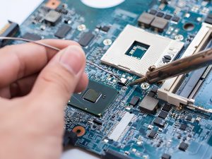
Wire bonding gold wire is a fine gold wire used to connect a chip, die, sensor, module, or substrate pad when standard soldering is not the best connection method. This blog mainly explains how wire bonding gold wire is used in high-reliability PCB and PCBA projects, what process, material, and surface finish requirements should be checked, and how EBest Circuit (Best Technology) supports engineering review, PCB fabrication, PCBA assembly, and testing.
EBest Circuit (Best Technology) supports high-reliability PCB and PCBA projects that involve wire bonding requirements, including PCB fabrication, surface finish review, DFM checking, PCBA assembly, component sourcing, testing, and production traceability. If your project needs a bondable PCB, ceramic substrate, RF module board, sensor board, or high-reliability assembly, you can send Gerber files, BOM, drawings, and requirements to sales@bestpcbs.com for engineering review.
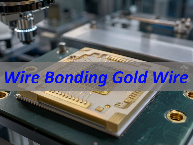
What Is Wire Bonding Gold Wire?
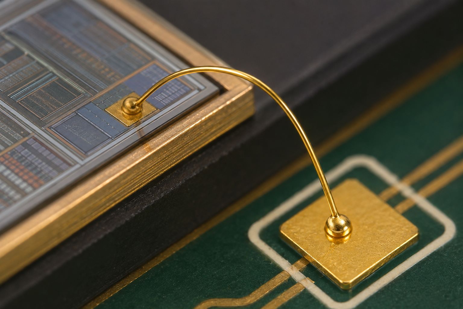
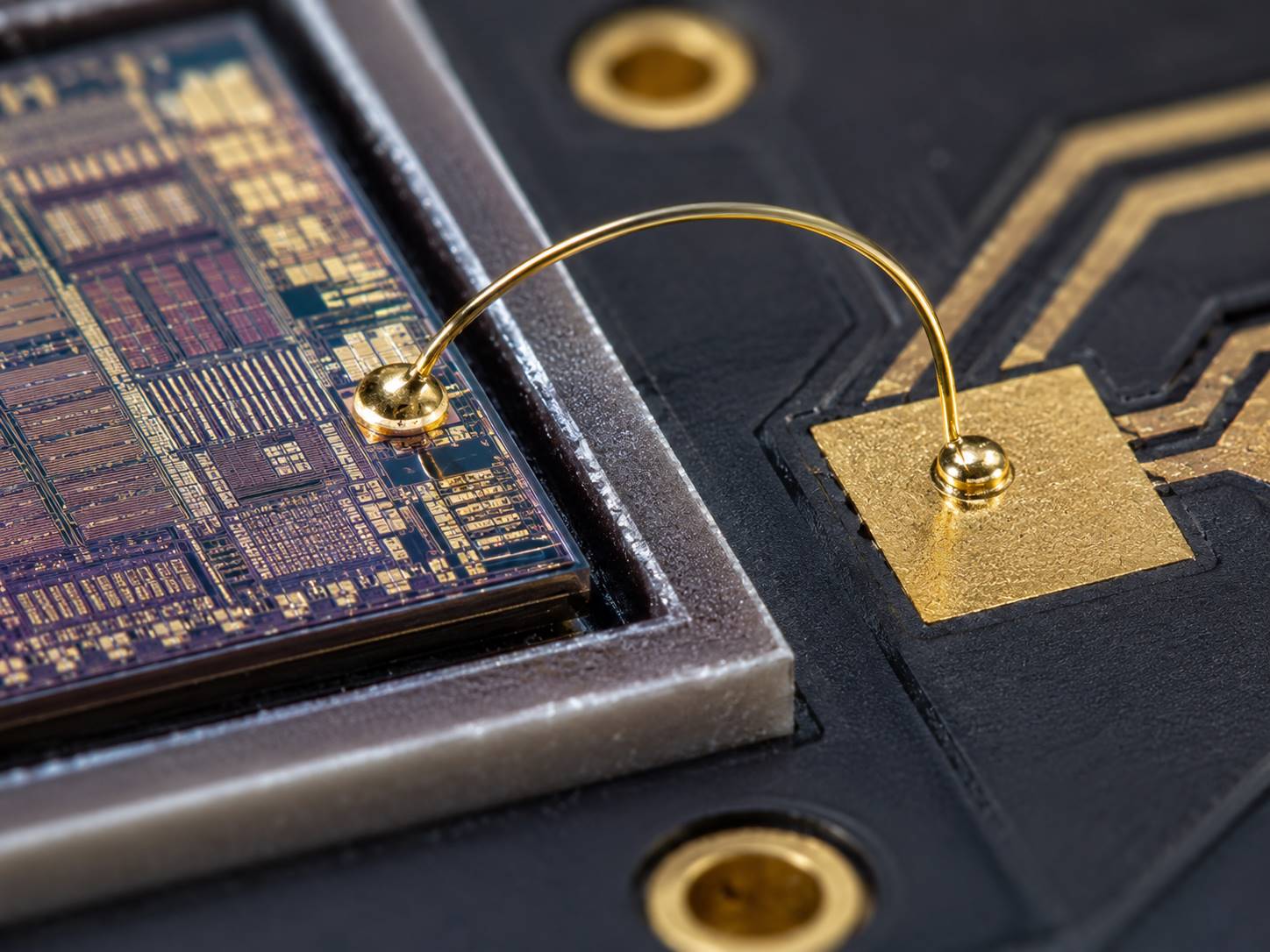
Wire bonding gold wire is a very thin gold wire used to make electrical connections between a small electronic device and a circuit pad. It is common when the design uses bare die, chip-on-board, hybrid circuits, sensors, RF modules, or special high-reliability packages.
In simple words:
- It works like a tiny bridge.
It connects the chip or die to the PCB, ceramic substrate, package, or module pad. - It is used where soldering is not suitable.
Some chips are too small, too delicate, or too specialized for normal SMT soldering. - It needs a bondable surface.
The PCB pad cannot be treated like a normal soldering pad only. The surface finish must be suitable for wire bonding. - It is part of the whole PCB/PCBA design.
Gold wire bonding is not just a material choice. It affects pad design, surface finish, substrate material, assembly process, and testing.
Common project types include:
- Bare die assembly
Used when a chip is mounted directly on a board or substrate. - Ceramic substrate modules
Used in high-heat, high-power, RF, sensor, and precision circuits. - RF and microwave modules
Used where short and stable electrical paths are important. - Medical and industrial electronics
Used when reliability, traceability, and long service life matter. - Automotive and aerospace electronics
Used in demanding environments where process stability is important.
For customers, the main point is this: if your project needs gold wire bonding, the PCB must be designed and manufactured for it from the beginning.
EBest Circuit (Best Technology) can review bonding pad design, PCB material, surface finish, stack-up, solder mask clearance, and assembly requirements before production. This helps reduce trial-and-error during prototype and batch production.
Why Is Gold Used in Wire Bonding for Electronics and IC Chips?
Gold is used because it is easy to bond, stable, conductive, and resistant to oxidation. For many high-reliability electronics, these properties make gold bonding wire a dependable choice.
Gold is selected for several clear reasons:
- Good electrical conductivity
Gold helps signals and current pass through fine connections with stable performance. - Strong oxidation resistance
Gold does not easily form an oxide layer, so the bonding surface stays more stable. - Good ductility
Gold wire can be shaped into loops and bonded without breaking easily. - Mature bonding process
Gold ball bonding is widely used and well understood in microelectronics manufacturing. - Reliable long-term performance
It is suitable for products that need stable operation over long service life.
Gold wire bonding is often used in:
- IC chips
- Sensor modules
- RF devices
- Hybrid circuits
- Ceramic substrates
- Optoelectronic modules
- Medical electronic modules
- Automotive sensors
- Aerospace electronics
- Industrial control modules
For PCB and PCBA buyers, the important question is not only “Why use gold?” The better question is:
Can the PCB pad, surface finish, and assembly process support stable gold wire bonding?
That is where manufacturing support becomes important. EBest Circuit (Best Technology) can help customers check whether the board material, pad finish, and production documents match the bonding requirement before the PCB is fabricated.
How Does the Gold Wire Bonding Process Work?
Gold wire bonding connects one pad to another using heat, pressure, ultrasonic energy, and a fine gold wire. The process sounds complex, but the basic idea is simple: press the gold wire onto a clean metal pad and create a stable metal-to-metal connection.
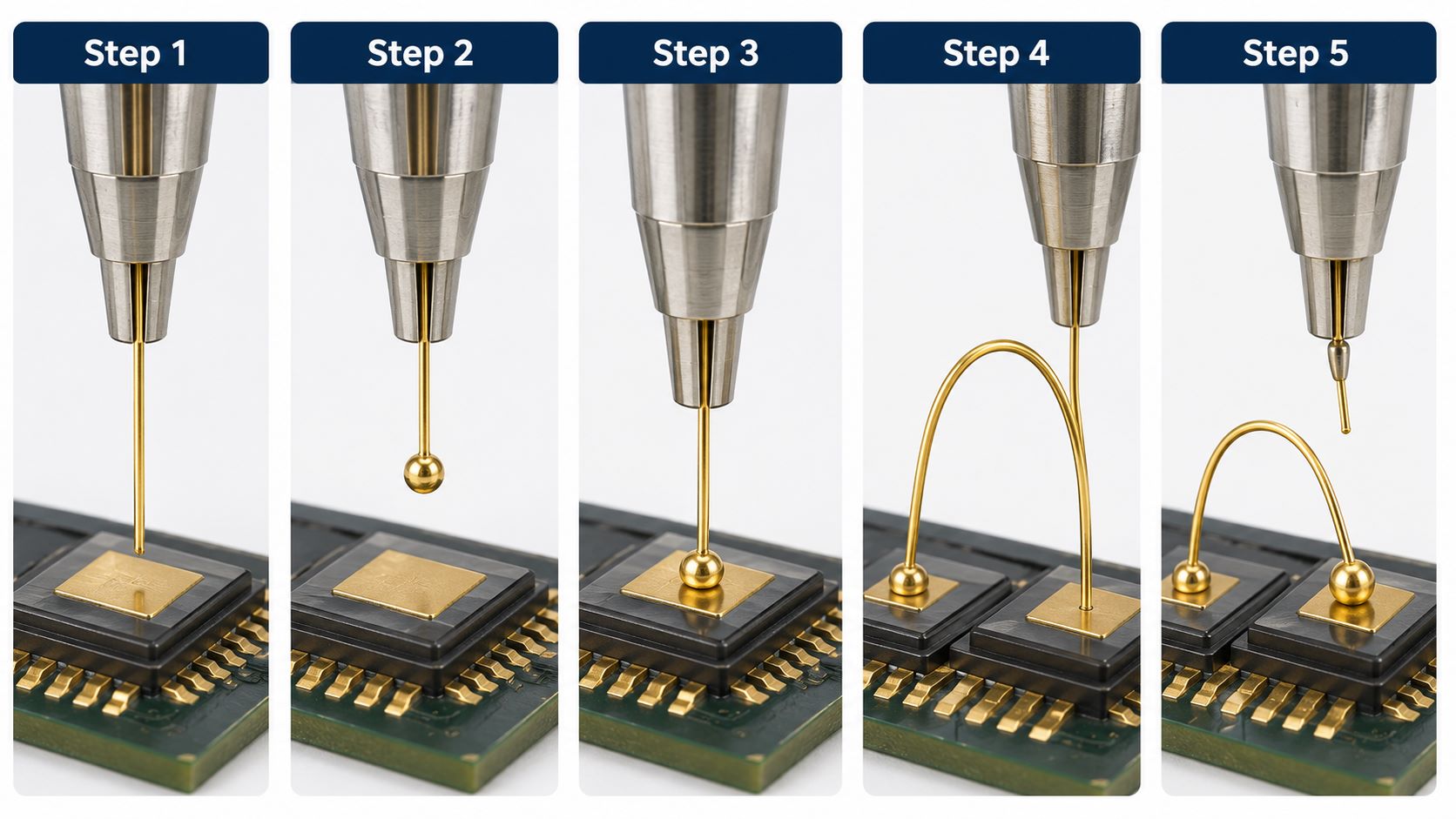
A typical gold ball wire bonding process works like this:
- Step 1: The gold wire is fed through a bonding tool.
The tool guides the wire to the correct pad position. - Step 2: A small gold ball is formed.
The end of the wire is melted into a tiny ball. - Step 3: The first bond is made.
The gold ball is pressed onto the chip pad or substrate pad. - Step 4: The wire loop is formed.
The machine moves to the second pad and creates a controlled wire loop. - Step 5: The second bond is made.
The wire is bonded to the second pad, then cut.
The quality of this process depends on a few practical factors:
- Pad surface must be clean.
- Pad finish must be bondable.
- Pad size must match the wire and tool.
- Substrate must stay stable during bonding.
- Wire loop height must have enough clearance.
- Bonding parameters must be controlled.
- Inspection and testing must confirm bond quality.
For a PCB project, these details should be confirmed before production. If the board is already made with the wrong finish or poor pad design, bonding problems may appear during assembly.
EBest Circuit (Best Technology) supports this stage through DFM review, fabrication drawing review, surface finish checking, PCB manufacturing, PCBA assembly, and testing coordination. For high-reliability projects, MES traceability can also help track materials, production status, and quality records.
Gold Ball Wire Bonding vs Gold Wedge Wire Bonding: What Is the Difference?
Gold ball wire bonding and gold wedge wire bonding are two common bonding methods. The main difference is the tool shape, bond shape, loop style, and application.
| Item | Gold Ball Wire Bonding | Gold Wedge Wire Bonding |
|---|---|---|
| Tool | Capillary | Wedge tool |
| First bond | Ball-shaped | Wedge-shaped |
| Speed | Usually faster | Usually slower |
| Direction | More flexible | More directional |
| Loop profile | Medium or higher loop | Lower loop possible |
| Common use | IC packaging, chips, sensors | RF, power modules, special layouts |
Gold ball wire bonding is common in IC packaging and microelectronics because it is fast, mature, and flexible. It works well when many fine connections are needed.
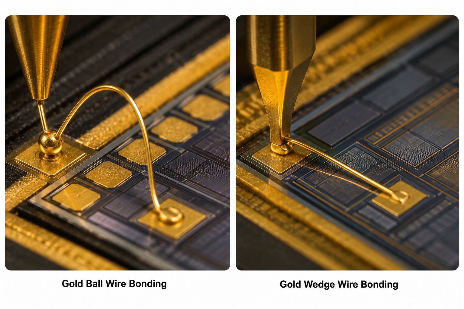
Gold wedge wire bonding is often used when the design needs a lower wire loop or more controlled wire direction. It can be useful in RF modules, power devices, and compact circuits.
For PCB design, the bonding method affects:
- Pad size
- Pad spacing
- Pad orientation
- Wire loop height
- Clearance around the bonding area
- Surface finish requirement
- Inspection method
A simple rule:
Ball bonding is often chosen for speed and flexibility. Wedge bonding is often chosen for low-profile or special layout control.
EBest Circuit (Best Technology) can help customers review the PCB layout based on the expected bonding method. This includes checking pad opening, solder mask clearance, material stability, and whether the board structure is suitable for the assembly process.
What Temperature and Surface Finish Are Needed for Gold Wire Bonding?
Gold wire bonding needs the right temperature and the right pad surface. The exact process window depends on the bonding machine, wire size, pad material, substrate, and reliability requirement.
For customers, the most important point is this:
A normal solderable PCB surface is not always suitable for gold wire bonding.
Surface finish must be selected carefully.
Common surface finishes related to wire bonding include:
| Surface Finish | Key Point |
|---|---|
| Electrolytic soft gold | Common for bondable gold pads |
| ENEPIG | Often suitable for soldering and wire bonding |
| ENIG | Must be reviewed carefully |
| Nickel gold | Can work when thickness and process are controlled |
| Thick gold plating | Used when stronger bondable gold layer is needed |
When choosing the surface finish, check these items:
- Gold thickness
The gold layer must be suitable for bonding, not only for corrosion protection. - Gold hardness
Soft gold is often preferred for bonding because it forms a better bond. - Nickel layer quality
Nickel can act as a barrier layer, but poor plating may affect reliability. - Pad cleanliness
Contamination can weaken the bond. - Solder mask clearance
The bonding tool needs enough open space around the pad. - Storage and packaging
Bonding surfaces should be protected from scratches, oxidation, and contamination.
Different PCB materials also behave differently during bonding:
- FR4 PCB
Suitable for many standard electronic products. For bonding projects, heat resistance and dimensional stability should be checked. - High-Tg FR4 PCB
Better for projects with higher thermal stress or stricter assembly requirements. - Ceramic PCB
Suitable for high heat, high power, sensor, RF, and precision applications. - Metal core PCB
Used for thermal management in LED, power, and high-current products. - RF PCB
Used when signal behavior and controlled dielectric performance matter. - Rigid-flex PCB
Used when the product needs a compact structure and flexible connection.
EBest Circuit (Best Technology) can manufacture and assemble multiple board types, including FR4 PCB, high-Tg PCB, ceramic PCB, aluminum PCB, copper substrate PCB, RF PCB, rigid-flex PCB, and multilayer PCB. For wire bonding-related projects, our team can review surface finish, pad design, material choice, and assembly notes before production.
How Do Gold, Aluminum, and Copper Wire Bonding Compare?
Gold, aluminum, and copper can all be used for wire bonding. Each material has its place. The right choice depends on the pad material, product requirement, current load, cost target, and reliability level.
| Material | Main Strength | Typical Consideration |
|---|---|---|
| Gold | Stable and easy to bond | Higher material cost |
| Aluminum | Cost-effective for many power uses | Oxidation control matters |
| Copper | Good conductivity and lower cost | Process control is stricter |
Gold wire bonding is often selected when reliability, corrosion resistance, and process stability are important.
Best-fit applications include:
- IC chips
- Sensors
- RF modules
- Medical electronics
- Aerospace electronics
- Ceramic substrate modules
- High-reliability assemblies
Aluminum wire bonding is common in power devices and some wedge bonding applications.
Best-fit applications include:
- Power modules
- Automotive power electronics
- High-current devices
- Some semiconductor packages
Copper wire bonding is used when conductivity and cost control are important, especially in high-volume semiconductor packaging.
Best-fit applications include:
- Consumer IC packages
- High-volume electronics
- Cost-sensitive semiconductor products
The decision should not be based only on wire price. A good material choice should consider:
- Bond pad material
- Surface finish
- Operating temperature
- Current requirement
- Product life cycle
- Vibration or shock
- Thermal cycling
- Inspection method
- Batch quantity
- Reliability test standard
For PCB and PCBA projects, the bonding wire must match the board finish and assembly process. EBest Circuit (Best Technology) can support early engineering review so the PCB is manufactured with the correct pad finish, material structure, and process notes.
How to Choose Gold Bonding Wire by Diameter, Resistance, and Cost?
Choosing gold bonding wire is mainly about three things: wire size, electrical performance, and project cost. The goal is not to choose the thinnest or cheapest wire. The goal is to choose a wire that works reliably with the PCB, pad, chip, and assembly process.
When reviewing gold bonding wire, focus on these points:
- Wire diameter
Thin wire is useful for small pads and fine-pitch designs. Thicker wire can carry more current and provide stronger mechanical performance. - Pad size
The pad must be large enough for the selected wire and bonding tool. - Current requirement
Higher current may need larger wire, shorter loop length, or better heat dissipation. - Wire length
Longer wires may increase resistance and inductance. - Loop height
Lower loops help save space. Controlled loop shape is important in RF and compact modules. - Resistance
Fine wire still has measurable resistance. This matters in precision circuits and power-related designs. - Inductance
In RF designs, bond wire length and loop shape can affect signal performance. - Cost
Gold wire cost is influenced by gold price, wire diameter, purity, supplier, and usage volume.
A practical selection path:
- Confirm the chip or die pad material.
- Confirm the PCB or substrate pad finish.
- Define current and signal requirements.
- Choose suitable wire diameter.
- Check pad size and spacing.
- Review loop height and clearance.
- Confirm bonding process and inspection method.
- Validate with sample production before batch orders.
For buyers, this means one thing:
Do not only ask for a PCB quote. Tell the manufacturer that the board is for gold wire bonding.
This allows the engineering team to check the right details from the beginning.
EBest Circuit (Best Technology) can support customers from prototype to production with:
- PCB fabrication
- PCBA assembly
- DFM review
- Surface finish review
- Material selection
- Component sourcing
- AOI, X-ray, electrical testing, and functional testing support
- ISO 13485 quality management for medical-related projects
- MES-based production traceability
- Engineering support for high-reliability applications
This is especially useful for medical, industrial control, automotive electronics, communication equipment, aerospace, RF, sensor, LED, and power electronics projects.
FAQs About Wire Bonding Gold Wire
1. What is wire bonding gold wire used for?
It is used to connect chips, dies, sensors, modules, or substrates to circuit pads. It is common in IC packages, ceramic substrates, RF modules, sensor boards, and high-reliability electronic assemblies.
2. Is gold wire bonding the same as soldering?
No. Soldering uses solder to attach packaged components to PCB pads. Gold wire bonding uses fine wire to connect a chip or die directly to a pad.
3. Does every PCB support gold wire bonding?
No. The PCB must have suitable pad design, surface finish, cleanliness, material stability, and bonding area clearance.
4. What surface finish is usually used for gold wire bonding?
Electrolytic soft gold and ENEPIG are commonly considered. ENIG may need special review because standard ENIG is not always suitable for wire bonding.
5. Can FR4 PCB be used for gold wire bonding?
Yes, in some projects. The key is to check temperature, flatness, pad finish, and reliability requirements. For higher thermal or precision requirements, ceramic PCB or other special materials may be better.
6. Why is ceramic PCB often mentioned with gold wire bonding?
Ceramic PCB has good thermal conductivity, dimensional stability, and high-temperature resistance. That makes it suitable for sensors, power modules, RF devices, LED modules, and hybrid circuits.
7. What is 1 mil gold bond wire?
1 mil gold bond wire has a diameter of about 0.001 inch, or around 25.4 microns. It is a common size in microelectronics, but the final size depends on pad design, current, and reliability needs.
8. Is gold wire better than copper wire?
Gold is easier to bond and more resistant to oxidation. Copper has good conductivity and lower material cost, but it needs stricter process control. The better choice depends on the project.
9. What files should I send for a project involving gold wire bonding?
Send Gerber files, fabrication drawing, stack-up, BOM, assembly drawing, bonding diagram, pad requirements, surface finish notes, and testing requirements.
10. Can EBest Circuit (Best Technology) support PCB and PCBA projects involving wire bonding requirements?
Yes. EBest Circuit (Best Technology) can support PCB fabrication, PCBA assembly, DFM review, material selection, surface finish review, testing coordination, and production traceability for high-reliability PCB and PCBA projects.
11. What board types can EBest Circuit (Best Technology) support?
We support FR4 PCB, high-Tg PCB, ceramic PCB, aluminum PCB, copper substrate PCB, RF PCB, rigid-flex PCB, multilayer PCB, heavy copper PCB, and related PCBA assembly projects.
12. How can I get an engineering review?
You can send your Gerber files, BOM, drawings, and project requirements to sales@bestpcbs.com. Our team will review the PCB design, material, surface finish, assembly needs, and quotation details.
Need support for a wire bonding-related PCB or PCBA project?
Send your files to sales@bestpcbs.com. EBest Circuit (Best Technology) can help review manufacturability, surface finish, assembly process, testing needs, and production feasibility before you move forward.