GND earth is a common phrase in electronics discussions, but it can create confusion when a PCB project moves from schematic review to manufacturing. Some teams use it to mean signal ground. Some use it to mean chassis ground, protective earth, shield ground, or a connection point between the board and metal enclosure.
For PCB and PCBA projects, the important question is practical: how should the approved ground notes be built, soldered, inspected, and tested without changing the customer’s circuit intent? EBest Circuit (Best Technology) supports PCB fabrication, component sourcing, PCBA assembly, grounding-related DFM review, inspection, and testing coordination. If your project includes GND earth notes, shield pads, mounting holes, connector shells, enclosure contact, or assembly requirements, please send your Gerber files, stackup, BOM, drawings, and notes to sales@bestpcbs.com for engineering review before production.
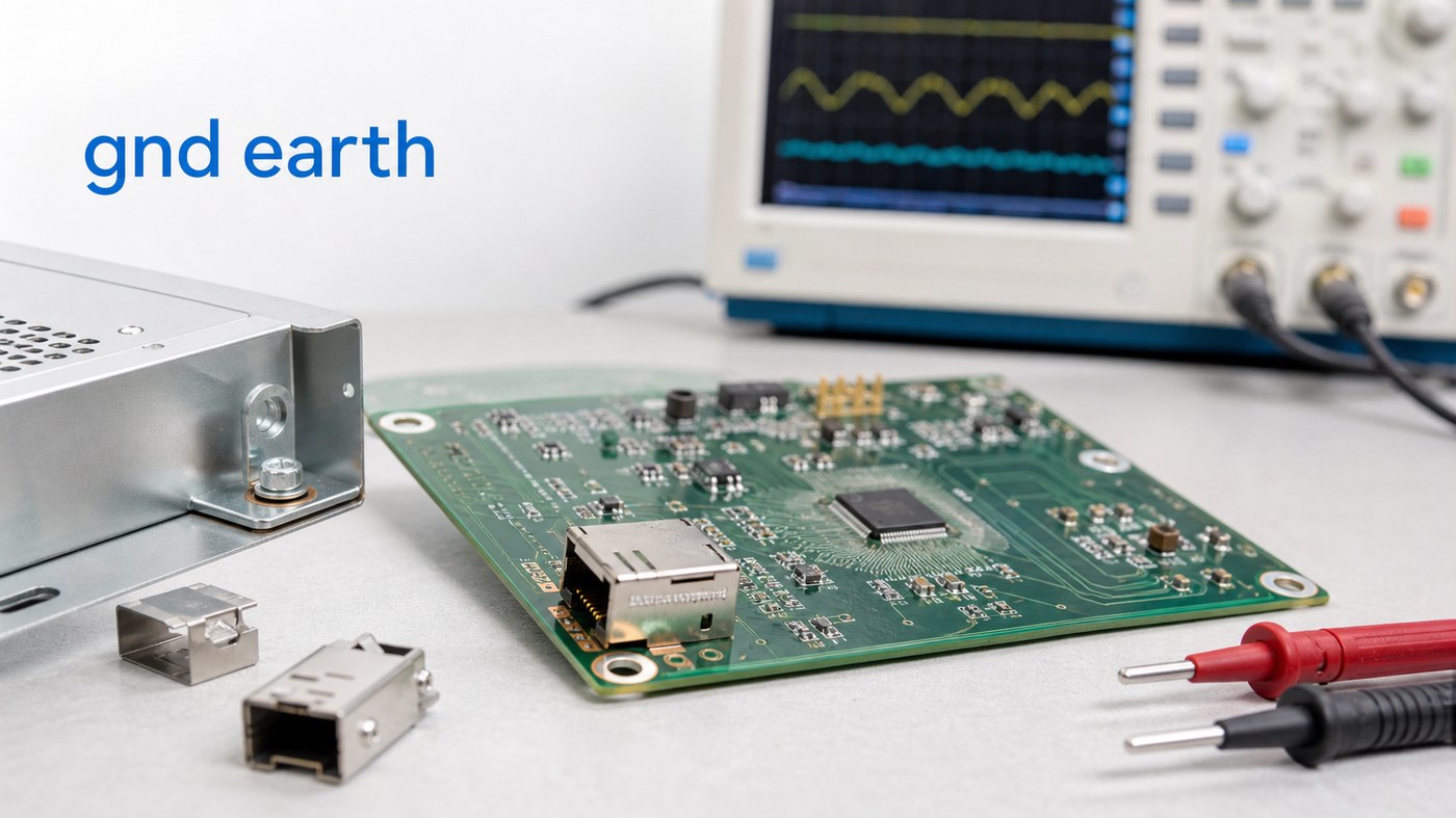
GND Earth Meaning in PCB and PCBA Projects
In many PCB files, GND earth is not a single universal net name. It is often a shorthand used by customers to describe how the board ground should relate to earth, chassis, cable shield, enclosure, or equipment safety ground.
The term may appear in several places:
- schematic net names such as GND, EARTH, PE, CHASSIS, or SHIELD
- PCB layout notes around mounting holes and connector shells
- mechanical drawings for enclosure contact
- assembly notes for screws, terminals, brackets, or shield cans
- test requirements for continuity or isolation checks
The PCB manufacturer should not decide the grounding scheme for the customer. The customer controls the electrical design. The manufacturer’s role is to keep the approved net names, copper areas, solder mask openings, plated holes, connector pads, and inspection notes consistent during fabrication and assembly.
GND vs Earth vs Chassis Ground
GND, earth, and chassis ground can be connected in some products and separated in others. The right choice depends on the customer’s circuit design, safety requirement, enclosure, cable system, and compliance target.
| Term | Common Meaning |
|---|---|
| GND | Board reference ground or return path |
| Earth | Protective earth or building/equipment earth |
| Chassis ground | Metal enclosure or frame reference |
| Shield ground | Cable shield or connector shell reference |
A low-voltage sensor board may only need a normal PCB ground net. An industrial controller may also need chassis contact. A product connected to long cables may need shield grounding near the connector. A mains-powered device may include protective earth requirements that must be defined by the customer’s safety design.
For manufacturing, ambiguity is the risk. If a drawing says “connect to earth” but the Gerber file shows an isolated mounting hole, production should stop for clarification before the board is built.
PCB Ground Planes and Return Paths
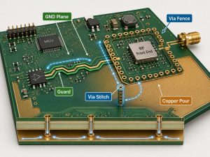
A PCB ground plane gives signals and power circuits a stable return path. Poor grounding is not only a schematic issue. It can show up as noisy measurements, unstable communication, EMI problems, poor RF performance, or inconsistent test results.
During manufacturing review, ground-related files should make these points clear:
- which layers contain ground planes
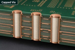
- which mounting holes are plated or isolated
- which connector shell pads connect to ground or shield
- whether copper is exposed for chassis contact
- whether solder mask openings are intentional
- whether impedance-controlled traces have the correct reference layer
For high-speed, RF, or communication boards, the ground reference affects signal behavior. When the board uses an RF PCB structure or controlled impedance routing, stackup, dielectric thickness, copper thickness, solder mask, and reference plane continuity should be checked before production.
Connector Shield Ground and PCB Ground Pads
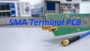
Connectors are one of the most common places where GND earth questions become manufacturing details. USB, Ethernet, CAN, RF, and industrial connectors may include a metal shell, shield pins, mounting tabs, or enclosure contact.
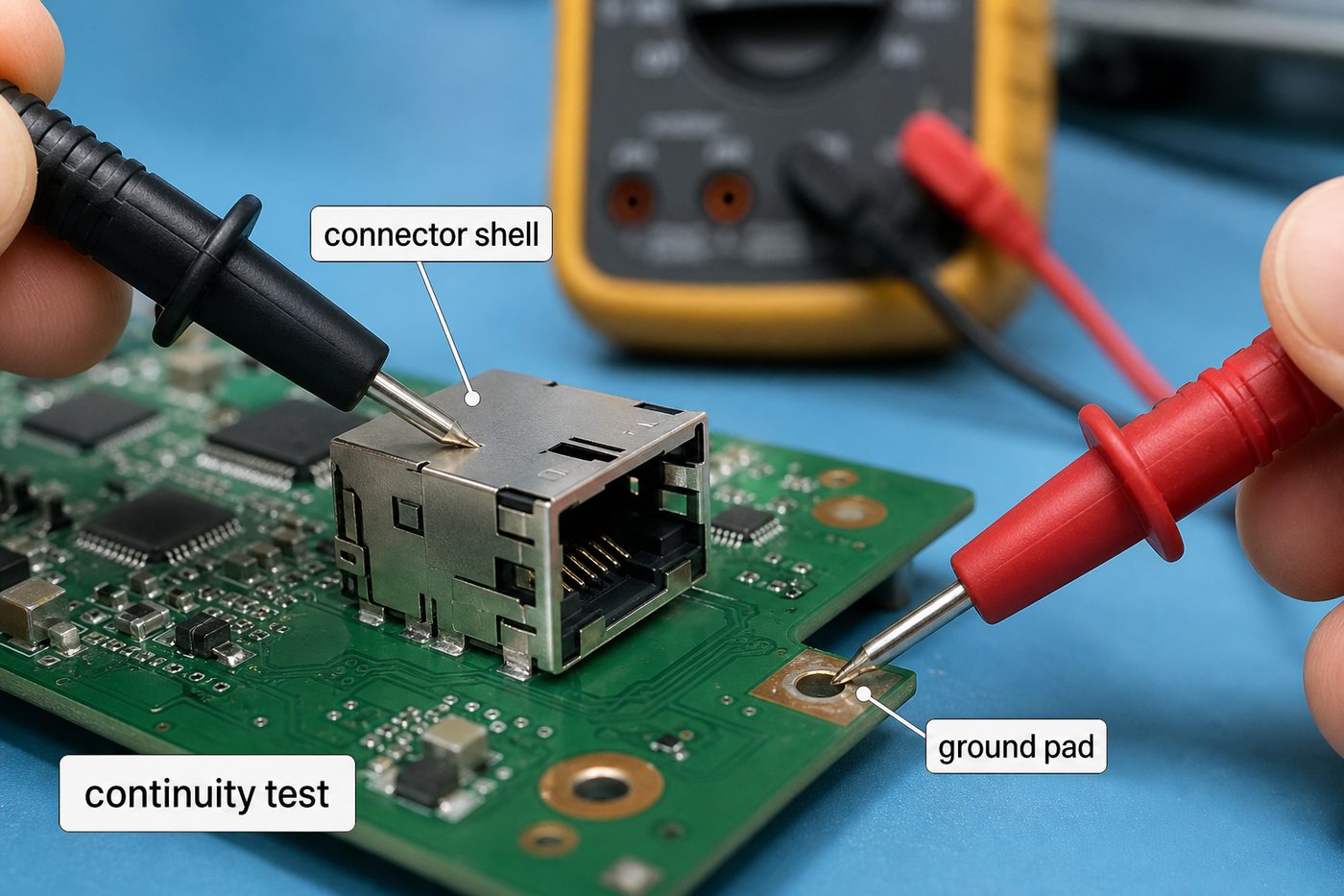
Important connector-area checks include:
- connector shell pad size and location
- solder mask opening around shield pads
- through-hole tab plating and annular ring
- clearance between shield pads and nearby copper
- mechanical support during plugging and unplugging
- continuity or isolation test requirements
Some connector shells are tied directly to board ground. Some connect through a controlled network. Some remain isolated from signal ground. The PCB supplier should not change that relationship. However, the supplier should check whether the footprint, plating, soldering method, and inspection notes are clear enough for production.
When a connector requires plug-in strength or manual soldering, the assembly plan may also involve through-hole assembly support in addition to SMT.
Mounting Hole Earth and Chassis Contact
Mounting holes are another common source of grounding mistakes. A mounting hole can be connected to GND, connected to chassis ground, connected through a component network, or completely isolated. The drawing and PCB files must show which condition applies.
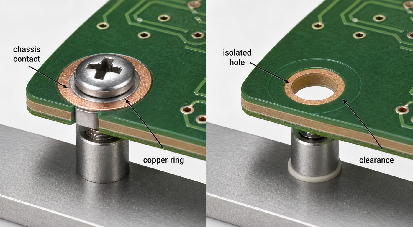
For mounting-hole grounding, EBest Circuit checks practical details such as:
- plated or non-plated hole requirement
- annular ring and copper exposure
- solder mask opening around the screw area
- clearance to other copper nets
- washer or screw contact area
- board thickness and mechanical tolerance
- panelization and tooling-hole influence
If the product relies on enclosure contact, the board surface should support stable mechanical and electrical contact. If the hole is intended to stay isolated, copper clearance and solder mask should help prevent accidental contact during assembly.
When GND Earth Affects EMI, ESD, and Safety
GND earth decisions often become important when the product has cables, shielding, metal housing, high-speed interfaces, high current, or external power. These products may need more careful grounding review before production.
Common project situations include:
- shielded cable termination near a connector
- metal enclosure contact through screws or brackets
- ESD discharge path from connector shell to chassis
- EMI shielding can soldered to PCB ground pads
- separation between noisy power ground and sensitive signal ground
- earth-related notes for equipment or enclosure assembly
If the board uses shielding cans or board-level shielding structures, the related topics of PCB EMI shield and EMI shield PCB manufacturing become relevant. The same grounding decision can affect pad design, soldering quality, mask opening, inspection, and enclosure assembly.
GND Earth Notes in Gerber, Drawing, and Assembly Files
Grounding instructions should not live only in one file. If the schematic, Gerber, drawing, BOM, and assembly notes do not agree, the supplier may need an engineering question before production starts.
Useful production files include:
- Gerber or ODB++ files
- PCB fabrication drawing
- stackup drawing
- BOM and approved component list
- CPL or pick-and-place file
- connector datasheets
- mechanical drawing or enclosure notes
- test requirements for continuity, isolation, or function
A short note such as “earth pad must contact enclosure” is helpful, but it should match the actual copper, solder mask opening, mounting hardware, and assembly method. Clear notes reduce back-and-forth and help keep prototype PCB assembly moving without avoidable questions.
GND Earth Manufacturing Case Study
A European industrial electronics customer needed a small-batch control board used inside a metal enclosure. The PCB included connector shield pads, mounting holes near the enclosure wall, and a customer note requiring selected points to maintain chassis contact after assembly.
Project requirements:
- Application: industrial control module
- Build stage: prototype validation before small-batch production
- PCB type: multilayer FR4 PCB with PCBA assembly
- Connector area: shield pads and metal shell contact
- Mechanical area: selected mounting holes for enclosure contact
- Inspection: visual inspection, soldering inspection, and continuity checks
- Packing: single-unit protection for assembled boards
Main challenge:
The customer’s concern was not only whether the board could be fabricated. The real risk was that connector shield pads, mounting holes, solder mask openings, and final assembly notes could be interpreted separately. One unclear grounding note could create rework after the board was already assembled into the enclosure.
EBest Circuit solution:
- Reviewed the Gerber files, drawing, BOM, and assembly notes together.
- Checked whether mounting-hole copper exposure matched the enclosure-contact requirement.
- Confirmed connector shell pad solderability before SMT and hand soldering.
- Kept grounding-related inspection notes visible during PCBA production.
- Arranged continuity checks for the customer-defined contact points.
Result:
The customer received assembled boards with the grounding notes, connector shell soldering, enclosure-contact areas, and inspection requirements controlled in one workflow. For this kind of project, the value is practical: the grounding details are checked before the board reaches the customer’s enclosure test bench.
What EBest Circuit Checks Before PCB and PCBA Production
EBest Circuit is suitable for GND earth PCB and PCBA projects when the customer needs manufacturing review, assembly coordination, and inspection support rather than only bare board fabrication.
Before production, the team can review:
- Gerber, ODB++, drawing, BOM, and assembly file consistency
- ground plane and reference layer requirements
- mounting-hole plating, mask opening, and chassis-contact notes
- connector shell pads and shield terminal soldering
- controlled impedance notes when signal return path matters
- SMT, through-hole, and manual soldering requirements
- continuity, isolation, functional testing, or inspection notes
- packing requirements for assembled boards
EBest Circuit has worked in PCB and PCBA manufacturing since 2006 and supports PCB fabrication, component sourcing, SMT assembly, testing coordination, and small-batch production. For grounding-sensitive boards, the useful support is not a generic checklist. It is keeping the customer’s approved grounding notes visible from file review to final delivery.
FAQs About GND Earth
1. Is GND earth the same as PCB ground?
Not always. PCB ground usually means the board reference ground. GND earth may refer to earth, chassis, shield, or a defined connection between the PCB and enclosure.
2. Should PCB GND connect to earth ground?
That decision belongs to the customer’s electrical and safety design. The PCB manufacturer should follow the approved schematic, drawing, and assembly notes rather than changing the grounding scheme.
3. What should I mark in the PCB files for GND earth?
Mark the net name, mounting-hole requirement, connector shell grounding, copper exposure, solder mask opening, chassis contact, and any continuity or isolation test requirement.
4. Can mounting holes be connected to GND earth?
Yes, if the design requires it. They may also be isolated. The fabrication drawing should clearly define plated holes, copper rings, mask openings, and chassis-contact areas.
5. Why does GND earth matter in PCBA assembly?
Because grounding may depend on soldered connector shells, shield pads, screws, brackets, enclosure contact, and final testing. If these details are unclear, the assembled product may fail inspection or enclosure validation.
All in all, a gnd earth requirement should be treated as a production detail, not only a schematic label. If your PCB or PCBA project includes ground pads, shield terminals, mounting-hole contact, enclosure grounding, or continuity-test requirements, please send your Gerber files, stackup, BOM, drawings, and assembly notes to sales@bestpcbs.com. EBest Circuit can help review the manufacturing path before your boards move into production.