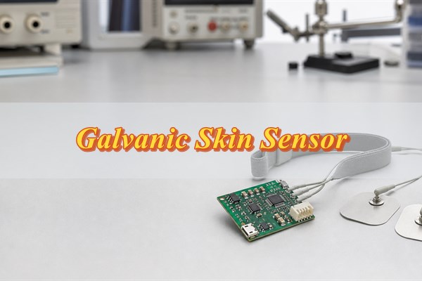
A galvanic skin sensor, often called a GSR sensor, measures electrodermal activity (EDA): changes in skin conductance produced through a two-electrode measurement path. It can track changes associated with sympathetic arousal, but it cannot identify a specific emotion by itself. Reliable data requires controlled electrode contact, adequate analog-front-end range, low PCB leakage, artifact detection and a repeatable validation method.
What Electrical Quantity Does a Galvanic Skin Sensor Measure?
Electrically, the sensor converts the skin-electrode resistance into conductance, the reciprocal quantity used for EDA measurement. The two electrodes, controlled excitation, analog front end and ADC form one measurement chain; sweat-gland activity changes the conductive path through the outer skin.
The conversion is:
G = 1 / R
where G is conductance in siemens and R is resistance in ohms. EDA is commonly reported in microsiemens (µS). If the circuit uses a known voltage, current can be converted to conductance. If it uses a known current, the measured voltage provides resistance and then conductance. In both cases, the electrodes and skin form a time-varying electrochemical interface rather than an ideal resistor.
EDA is most useful when conductance changes can be synchronized with a defined event or another measured channel. Typical uses include psychophysiology research, workload studies, usability testing and wearable sensing; EDA is an arousal-related input, not a stand-alone emotion label or diagnosis.
How Does a Galvanic Skin Sensor Measure Electrodermal Activity?
The sensor applies a controlled excitation, measures the skin-electrode response and converts that response into a conductance time series. Most EDA systems use an exosomatic method: the instrument supplies a small constant voltage or constant current instead of relying only on naturally occurring skin potential.
| Signal-Chain Stage | Engineering Task | Primary Failure Risk |
| Electrodes | Create repeatable skin contact | Pressure change, drying gel, motion or polarization |
| Excitation | Set a known voltage or current | Excessive stimulus, drift or loss of linear range |
| Analog front end | Convert and condition a high-impedance signal | Input bias, leakage, saturation and power noise |
| Low-pass filter | Limit out-of-band noise and aliasing | Removing real phasic content or retaining motion artifacts |
| ADC and firmware | Digitize, timestamp and quality-check samples | Insufficient range, resolution, synchronization or metadata |
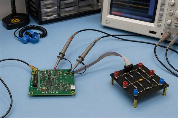
A constant-voltage design can measure current with a transimpedance stage or infer conductance from a divider. A constant-current design measures the voltage developed across the skin path. The chosen topology must keep the full expected impedance range inside the AFE and ADC limits. The Analog Devices AD5940 EDA example uses a resistor-capacitor test board to model skin, body, electrode and contact impedance and identifies a typical model range of approximately 20 kΩ to 10 MΩ. That range is a useful design stimulus for a bench fixture, not a universal human acceptance limit.
Which Electrodes and Body Locations Produce Usable EDA Data?
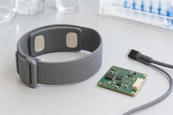
Electrode material, area, spacing, pressure and body location must be controlled together because each changes the skin-electrode interface. Laboratory systems often use Ag/AgCl gel electrodes on the palm or fingers, where eccrine sweat-gland density is high. Wearables commonly use dry metal electrodes on the ventral wrist because that position is practical, although it can be less sensitive and more dependent on strap pressure.
- Ag/AgCl gel electrodes: Often provide stable, low-noise laboratory contact, but gel can dry and shelf life must be managed.
- Dry metal electrodes: Support reusable wearables, but contact impedance changes more with motion, pressure, skin hair and fit.
- Electrode area: Affects current density and interface impedance; changing area between prototypes invalidates direct comparisons.
- Placement: Palms and fingers can provide strong responses but constrain activity; wrist placement improves wearability and increases artifact-control demands.
- Preparation: A protocol should define cleaning, settling time, strap force or adhesive method and replacement interval.
How Should Engineers Design the Analog Front End?
The analog front end must cover the expected skin and contact impedance without allowing bias current, PCB leakage, offset or interference to dominate the measurement. Start with the measurement range and excitation limit, then calculate the output at both conductance extremes. Select the topology, gain and reference voltage only after confirming headroom across supply, tolerance and temperature.
For constant-voltage excitation, calculate Imax = Vexc / Rmin and Imin = Vexc / Rmax, then size the sense element and gain so both currents remain measurable. For constant-current excitation, verify that Vmax = Iexc × Rmax stays within the compliance voltage and ADC range.
- Input bias and leakage: Choose amplifiers, switches and protection parts whose leakage remains small relative to the minimum measured current across temperature.
- Output headroom: Check dry-contact, open-electrode and highly conductive conditions so the amplifier and ADC do not silently clip.
- Reference stability: Excitation and ADC reference noise can appear as conductance change; use ratiometric measurement where the topology permits.
- Protection capacitance: ESD devices protect the user interface but add leakage and capacitance. Qualify the exact part in the intended range rather than copying a generic protection circuit.
- Range switching: If multiple feedback resistors are used, include switch leakage, charge injection and settling time in the error budget.
A published low-resource wearable design used an AFE followed by a fourth-order low-pass filter and designed its signal path for 0–1 Hz. That implementation is evidence that EDA is a slow signal; it is not a requirement that every product use the same filter order or cutoff. Define the passband from the intended tonic and phasic features, then verify the response with injected waveforms.
Which Sampling, Filtering and ADC Choices Preserve the EDA Signal?
Derive the sampling rate from the required passband, analog anti-alias filter and synchronization requirement. The Nyquist rate is only the mathematical lower bound: sample above twice the highest passed frequency with enough margin for the real filter transition, then verify that the ADC range preserves both dry-contact and high-conductance conditions without clipping.
Use the following decision chain to turn the required EDA features into measurable filter, ADC and data-quality requirements:
- Define the signal band: Specify the slow tonic trend and fastest phasic feature that the study or product must preserve; this becomes the input requirement for filtering and sampling.
- Set the analog cutoff: Choose the anti-alias filter from the highest wanted frequency and its real transition band, then verify attenuation before frequencies can fold into the EDA band.
- Calculate the sampling rate: Start above twice the highest passed frequency, add margin for the non-ideal filter transition and confirm that timing supports event alignment.
- Size the ADC range: Convert the dry-contact and high-conductance endpoints into expected AFE voltages so neither endpoint clips or disappears below the usable code range.
- Verify effective resolution: Include reference noise, amplifier noise, quantization, gain tolerance and digital filtering; nominal ADC bits alone do not prove that the smallest required conductance change is measurable.
- Preserve diagnostic evidence: Synchronize EDA with motion, temperature and event markers, and retain raw or minimally processed samples plus range and saturation status for artifact review.
Averaging can reduce random noise but can also smear a short phasic conductance response or hide a step caused by electrode motion. Document cutoff, order, phase behavior, edge handling and every removed segment so reviewers can reproduce the processing. A smooth plot is not proof of valid source data; compare filtered output with raw samples and synchronized artifact channels.
What Causes False Peaks, Drift and Saturation in Galvanic Skin Data?
False EDA events most often come from the electrode interface, motion, environment, range limits or power interference rather than the autonomic response being studied. A systematic review of EDA collection identifies motion, temperature variation and electrical noise as important confounders. Ambulatory measurement adds variable strap pressure, skin hydration and changing environmental conditions.
| Observed Pattern | Possible Cause | Next Check |
| Near-zero or flat signal | Open electrode, dry contact or broken lead | Measure contact continuity and test with a known resistor |
| Sudden step during movement | Pressure change or electrode slip | Compare accelerometer and strap/contact data |
| Slow baseline drift | Temperature, hydration, electrode polarization or leakage | Repeat with controlled environment and simulated impedance |
| Clipped high reading | AFE or ADC saturation, excessive sweating or conductive bridge | Inspect raw code, range state and electrode spacing |
| Periodic ripple | Power-line, switching regulator or digital coupling | Measure the spectrum and probe supplies/returns |
Compare each event with a protocol-specific baseline and synchronized artifact channels rather than applying one universal threshold. Any model that labels stress, emotion or pain must define its population, inputs, exclusions and validation method.
How Should a Galvanic Skin Sensor PCB Be Laid Out?
Protect high-impedance electrode and feedback nodes from leakage, return-current coupling, switching edges and contaminated surfaces. The exact stack-up and layout depend on topology, but the PCB review should trace every sensitive node from connector to AFE and every return path back to its source.
- Short sensitive paths: Place the AFE close to the electrode connector and keep high-impedance traces away from clocks, antennas, DC/DC switch nodes and high-current LED or motor paths.
- Defined returns: A four-layer board can simplify continuous reference planes, but layer count does not correct a broken return path. Separate noisy load currents by placement and routing, then connect analog and digital domains according to the converter and AFE reference architecture.
- Guarding: A driven or quiet guard can reduce surface leakage around a very high-impedance node, but only if its voltage, stability, clearance and test access are engineered for the circuit.
- Power filtering: Isolate AFE supply noise with a suitable regulator, local decoupling and controlled current loops. Verify startup and radio-transmit disturbances.
- Connector protection: Put ESD and current-limiting elements at the entry point while qualifying their leakage across temperature and humidity.
- Testability: Add accessible points for excitation, reference, AFE output, ground and digital timing without turning the sensitive node into a large contamination antenna.
Which PCBA Materials and Assembly Controls Protect High-Impedance Nodes?
Flux residue, moisture, fingerprints and unsuitable protective materials can create leakage paths comparable to the signal being measured. High-impedance performance must therefore be specified as an assembled-board requirement, not inferred from the bare PCB alone.
- Cleaning process: Define flux type, cleaning chemistry, rinse, drying and ionic-contamination acceptance appropriate to the assembly.
- Solder mask and spacing: Review mask dams, exposed copper, connector pads and creepage paths around the electrode input. Do not assume solder mask is a perfect insulator.
- Conformal coating: Select coating for the intended humidity and biocompatibility boundary, while keeping connectors, electrodes and test contacts properly masked.
- Protection components: Control approved manufacturer part numbers because substitution can change leakage and capacitance even when package and voltage rating match.
- Handling: Use gloves and controlled packaging for cleaned high-impedance assemblies; visual cleanliness does not prove electrical cleanliness.
- Environmental verification: Repeat leakage and zero-input tests at relevant temperature and humidity rather than qualifying only at room conditions.
Manufacturing documentation should identify sensitive nets, no-touch areas, cleaning requirements, coating keep-outs and functional-test limits. Release the assembly drawing, coating drawing and test specification under revision control so the supplier can trace each requirement to the approved build.
How Can Engineers Validate a Galvanic Skin Sensor Without a Human Subject?
Use a traceable resistor-capacitor network or impedance simulator to validate range, linearity, bandwidth and fault response before any human-subject work. This separates electronic performance from biological variability and allows repeatable regression testing.
- Zero and open input: Confirm the reported state, recovery behavior and absence of unsafe or undefined output.
- Resistance sweep: Apply known values spanning the intended range, including endpoints and range-switch boundaries.
- Dynamic step: Switch between known impedances and measure settling, overshoot and digital filter delay.
- Parallel capacitance: Add representative capacitance to model electrode and cable effects, then verify stability.
- Interference injection: Operate radios, displays, chargers and switching supplies while monitoring error and spectrum.
- Leakage stress: Repeat at temperature and humidity corners and after the specified assembly cleaning process.
- Fault tests: Exercise lead-off, shorted electrodes, reversed accessories, ESD protection behavior and ADC clipping.
- Golden-unit regression: Store raw results, fixture identification, firmware version and pass/fail limits for future builds.
Which Safety and Compliance Boundaries Apply to Skin-Contact Devices?
The applicable safety path follows intended use, claims, contact duration, power architecture and market classification; a research sensor and a medical device do not share the same release evidence. Begin by documenting whether the device only supports research or wellness observation, or whether it makes a diagnostic, monitoring or treatment claim.
For skin-contact materials, evaluate the finished electrode, gel, adhesive and exposed housing as one contact system under the intended contact type and duration. If the product enters a medical-device pathway, the biological evaluation plan may need to consider ISO 10993-1; a component data sheet alone is not finished-product evidence.
If the finished product is medical electrical equipment, IEC 60601-1 addresses general basic safety and essential performance, and collateral or particular standards may also apply. A bare-board functional pass is not system-level safety evidence. Battery charging while worn, USB connection, isolation, leakage current and accessory use require system-level review.
What Should Engineers and Buyers Include in an RFQ?
An RFQ should define the electrical range, electrode interface, PCB/PCBA build, firmware state and validation evidence instead of requesting only a board quantity. Incomplete inputs can produce a board that powers on but cannot meet leakage, noise or safety requirements.
- Design files: Gerber or ODB++, drill data, stack-up, schematic, BOM, centroid data and assembly drawings.
- Sensor interface: Electrode material, connector, cable, expected impedance range, excitation and contact configuration.
- Signal requirements: Bandwidth, sample rate, ADC range, resolution target, allowable drift, noise and settling time.
- PCB controls: Controlled sensitive nets, grounding approach, surface finish, cleanliness, coating and keep-out requirements.
- Programming: Firmware image, programming interface, configuration data, calibration constants and serialization needs.
- Functional test: Fixture circuit, resistance/capacitance points, pass limits, raw-data format and golden-unit procedure.
- Compliance context: Intended use, skin-contact duration, target markets and applicable safety or regulatory plan.
Require the supplier to return DFM findings, component-risk questions, test coverage and fixture responsibilities, together with every requirement that still needs engineering confirmation before the quotation is treated as final.
FAQs About Galvanic Skin Sensors
Q1: Should electrode contact quality be reported separately from EDA?
A1: Yes—contact quality should have its own status or confidence indicator. A lead-off flag, impedance check or stability score prevents downstream software from treating a detached or unstable electrode as physiological data.
Q2: Should the cable between the electrodes and PCB be shielded?
A2: Use shielding only after evaluating added capacitance, leakage and return-current effects. Compare noise and settling with the intended cable length, motion and connector rather than assuming that a shield always improves the signal.
Q3: How should calibration constants be stored?
A3: Version calibration constants by unit, hardware revision and firmware build. Protect them with a checksum or equivalent integrity check and retain the fixture ID and calibration date.
Q4: Which connector properties matter at the electrode input?
A4: Prioritize low leakage, cleanability, stable contact resistance and strain relief. Also verify touch safety, mating-cycle life and whether flux or coating can become trapped around the sensitive pins.
Q5: Can one analog front end multiplex several electrode pairs?
A5: Yes, but switch leakage, charge injection, crosstalk and settling become part of the error budget. Validate every channel and switching sequence across temperature and the full impedance range.
Q6: How should startup and electrode settling be handled?
A6: Define a settling interval and suppress interpretation until contact and AFE output meet stable criteria. Record any range changes or lead-off events that restart the interval.
Q7: Which telemetry helps diagnose field failures?
A7: Store raw ADC code, active range, saturation, lead-off status and timestamps. Motion, temperature, battery and charging state make intermittent contact and interference much easier to reproduce.
Q8: When does a new electrode accessory require revalidation?
A8: Revalidate after changes to material, area, spacing, gel, adhesive, cable or connector. These changes can alter impedance, polarization, motion sensitivity and the applicable skin-contact assessment.
Q9: How should engineers isolate a failed sensor board?
A9: Inject a known impedance and trace the result stage by stage. Compare excitation, AFE output, ADC code and firmware conversion against a passing unit to identify whether the fault is analog, conversion-related or computational.
Q10: How often should the production fixture be calibrated?
A10: Set the interval from component tolerance, drift history, usage and product risk. Include an out-of-tolerance response that identifies affected units and triggers containment or retest.
If you need PCB manufacturing or PCBA support, contact EBest Circuit at sales@bestpcbs.com and submit Gerber/ODB++, BOM, quantity, stack-up, assembly, programming and functional-test requirements so the engineering team can review manufacturability and test scope before quotation.