A fiber optic fpv drones PCB connects the flight controller, camera or video processor, optical transceiver, power regulation, sensors, and motor-control interfaces in a compact airborne electronics system. The fiber carries optical data, but the PCB still has to manage high-speed electrical signals, switching noise, heat, vibration, connector stress, and strict weight limits.
The design should therefore be treated as a coordinated set of signal, power, mechanical, and manufacturing decisions. This guide focuses on the PCB and PCBA engineering needed for lawful industrial, inspection, research, and communications applications. Exact data rates, environmental limits, interfaces, and acceptance tests must be defined for each project.
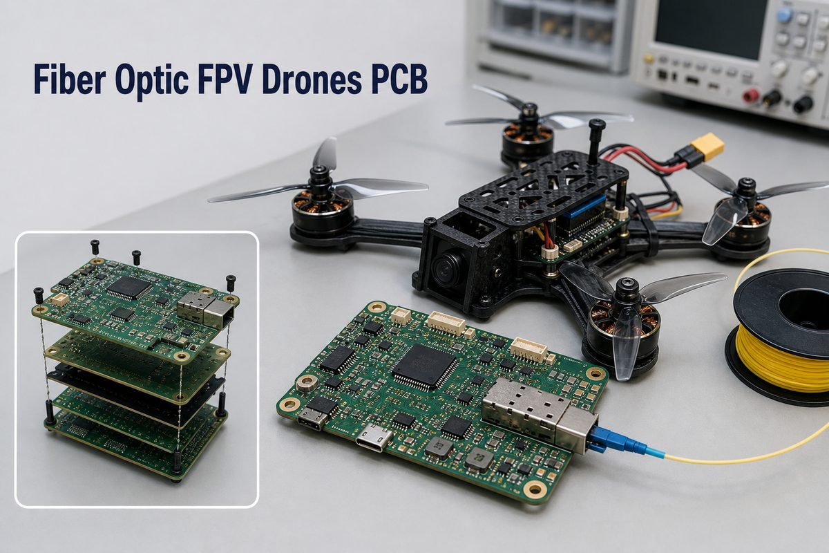
What Is a Fiber Optic FPV Drones PCB?
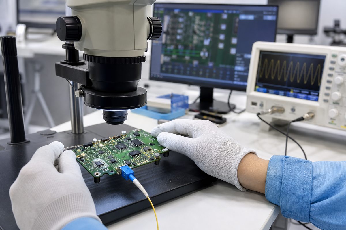
A fiber optic FPV drones PCB is the board-level platform that routes control and video data between the drone electronics and an optical communication module. It may be one integrated assembly or several boards connected as a flight-control stack, camera board, optical-interface board, power board, and electronic speed controller system.
The optical fiber does not carry electrical power to the aircraft. A battery and local regulators still power the processor, sensors, camera, transceiver, and other loads. The PCB must keep those rails stable while motors and switching converters create rapid current changes. It must also preserve the electrical channel between the processor or video interface and the optical transceiver.
How Does a Fiber Optic FPV Drone Work?
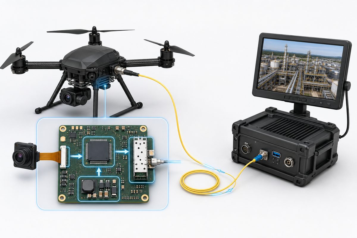
A fiber-linked FPV platform converts electrical control and video data into optical signals, sends them through a lightweight fiber, and converts them back at the opposite end. The exact phrase fiber optic fpv drone how it works often leads readers to the link itself, but reliable operation also depends on the electronics around that link.
- The camera and sensors create video and flight data.
- The flight controller processes commands and sensor inputs.
- An electrical interface passes selected data to an optical transceiver or conversion module.
- The transceiver converts electrical data to light for transmission through the fiber.
- The ground-side unit performs the reverse conversion for the display and controller.
This arrangement can remove the primary control/video path from a conventional radio link, but it does not make the complete aircraft immune to every disturbance or failure. Power noise, damaged connectors, excessive fiber bending, processor faults, sensor errors, and mechanical stress can still interrupt the system.
Which Circuit Boards and Functional Blocks Make Up the System?
The system normally combines flight control, video, optical communication, power conversion, sensing, and motor interfaces. These functions can share one board, but separating them may simplify noise control, thermal management, service, and mechanical placement.
| Board or Block | Main Function | PCB Design Focus |
| Flight controller | Processes sensor data and generates control outputs | Clean sensor power, stable clocks, short return paths, vibration-aware placement |
| Optical interface | Converts electrical data to and from optical signals | Differential routing, decoupling, connector retention, transceiver heat |
| Camera or video board | Captures and conditions the FPV image stream | High-speed interface integrity, low-noise power, compact interconnects |
| Power distribution and regulation | Feeds logic, camera, optical module, and peripheral rails | Current capacity, filtering, protection, thermal paths |
| ESC or motor interface | Drives or commands the motors | High-current loops, switching noise, MOSFET cooling, isolation from sensors |
For a broader system comparison, our guide to the types of circuit boards used in drones explains how flight-control, power, camera, sensor, and communication boards divide the work.
What Makes an FPV Drone PCB Board Different?
An fpv drone pcb board must operate under tighter weight, space, vibration, and power-noise constraints than many stationary electronics. In a fiber-linked design, the optical interface adds another high-speed data path and a mechanically sensitive connection near a moving platform.
- Mixed electrical environments: quiet sensors and high-speed data operate near motor switching and battery current.
- Mass and balance: board dimensions, copper weight, connectors, shields, and the fiber assembly affect mechanical integration.
- Limited cooling: airflow changes with enclosure, speed, board orientation, and nearby components.
- Continuous movement: vibration can fatigue solder joints, connectors, cables, and unsupported components.
- Service constraints: densely stacked boards need accessible test points and a clear replacement strategy.
These constraints should be set before schematic capture. Adding the optical module late can create blocked airflow, long data routes, poor connector access, or an unstable center of mass.
How Should an FPV Drone Controller PCB Handle the Optical Interface?
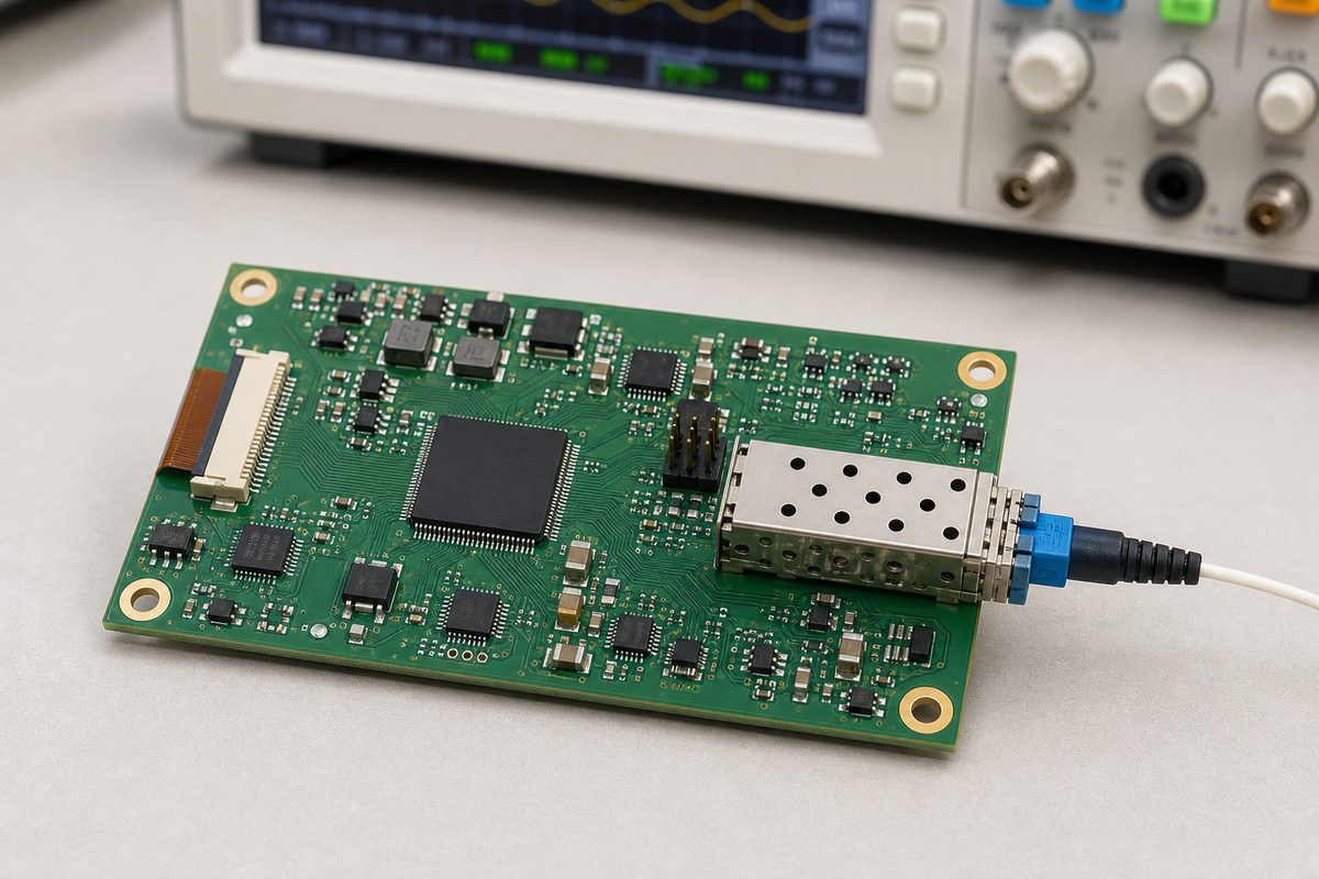
An fpv drone controller pcb should treat the optical transceiver as a high-speed electrical load with its own power, thermal, signal, and connector requirements. The fiber begins at the optical port; everything between the processor and that port is still an electrical PCB channel.
Start with the selected module datasheet and define its host interface, supply rails, peak current, reset behavior, clocking, connector, and thermal limits. Keep high-speed pairs short, maintain a continuous reference plane, and avoid stubs or unnecessary test pads. Place local decoupling close to supply pins and provide a low-inductance return path.
Connector orientation must be coordinated with the enclosure and fiber path. The optical connector or pigtail should not transfer repeated pull or twist directly into small solder joints. If the design uses a separate optical daughterboard, specify the board-to-board connector, retention method, mating cycle, and service access before layout.
How Should Power Domains Be Separated from Motor Noise?
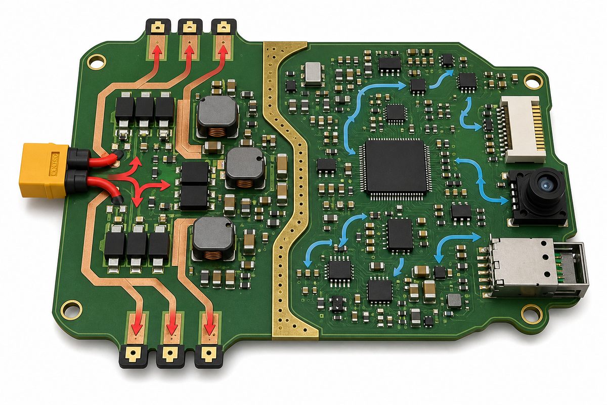
Power-domain planning should prevent motor and converter noise from disturbing the flight controller, camera, sensors, or optical interface. A single battery may feed every function, but that does not mean all loads should share the same unfiltered path.
- Keep high-current battery and motor loops physically compact.
- Separate sensitive regulators from switching nodes and hot power components.
- Use the regulator vendor’s recommended input, output, and compensation layout.
- Place high-frequency decoupling at the IC pins and bulk capacitance near load groups.
- Do not split a reference plane beneath a high-speed signal simply to create visual separation.
- Plan current return paths before routing signals between functional zones.
Power integrity should be checked during load transitions, not only at idle. The optical transceiver, processor, and camera may react differently to voltage droop or ripple. Test limits should come from the component datasheets and system specification rather than one generic ripple target.
How Should High-Speed Video and Control Data Be Routed?
High-speed routes should be designed as transmission lines whose geometry, return path, vias, and connector launches are controlled from the processor to the optical module. The required impedance and matching tolerance depend on the actual electrical interface and component datasheets.
Practical layout checks include:
- Define the stackup and target impedance with the PCB fabricator before final routing.
- Keep differential-pair geometry consistent and avoid abrupt neck-downs.
- Minimize stubs, layer changes, and unnecessary connector transitions.
- Add nearby return vias when a high-speed pair changes reference layers.
- Separate fast data from switching nodes, motor phases, and noisy clock sources.
- Reserve test access that does not create an unacceptable discontinuity.
Our high-speed digital PCB design guide covers stackup, return paths, differential routing, vias, crosstalk, and power integrity in more detail. When waveform margin matters, an eye diagram can be combined with TDR, channel measurements, and functional testing under defined conditions.
What Does the Fiber Optic FPV Drone Cable Change Mechanically?
The fiber optic fpv drone cable adds bend-radius, strain-relief, routing, connector, and spool-integration requirements that must be resolved with the PCB and enclosure. The board should not become the mechanical anchor for an unsupported fiber path.
Define the minimum bend radius, connector or pigtail geometry, retention method, exit angle, and allowable movement from the chosen fiber and module documentation. Keep the path away from sharp board edges, propulsive components, hot surfaces, and service fasteners. If a separate spool or dispensing assembly is used, its loads should be carried by the mechanical structure rather than small PCB pads.
Mechanical review should also cover assembly sequence. A connector that is electrically correct may be unusable if it cannot be mated after the boards are stacked. A short flexible interconnect or daughterboard may improve serviceability, but it adds connectors and possible signal discontinuities that require validation.
Which PCB Stackup and Materials Fit the Design?
The stackup should be chosen from routing density, electrical interface speed, power-current needs, board thickness, weight, and manufacturing tolerance. There is no universal layer count or laminate for every fiber-linked drone controller.
| Design Need | Possible PCB Direction | Decision Check |
| Compact controller with moderate routing density | Multilayer FR-4 | Reference planes, finished thickness, thermal margin, impedance feasibility |
| Fine-pitch processor or dense camera interface | HDI construction when justified | Escape routing, microvia structure, assembly yield, cost |
| Moving camera or constrained interconnect | Flexible or rigid-flex circuit | Bend zone, stiffener, dynamic-cycle requirement, connector reduction |
| Higher-current power section | Localized heavier copper or separate power board | Temperature rise, etching limits, weight, copper balance |
Controlled impedance requires agreement on dielectric thickness, copper thickness, trace geometry, and material properties. Our impedance control PCB guide explains how design targets connect to fabrication and test coupons.
How Should Vibration, Heat, and Environmental Exposure Be Managed?
Reliability starts with the actual mounting, airflow, duty cycle, temperature, humidity, and vibration profile. A coating or stronger material cannot compensate for unsupported connectors, poor thermal paths, or components placed in high-strain areas.
- Keep heavy components away from unsupported board edges where possible.
- Use mounting-hole and keep-out geometry that avoids local copper or laminate stress.
- Review connector retention and cable strain relief as part of the enclosure.
- Provide copper area and thermal vias for regulators, processors, and power devices when the package guidance requires them.
- Measure component temperatures in the real enclosure and operating airflow.
- Select conformal coating or sealing only after checking connectors, sensors, optical surfaces, rework, and service requirements.
Board cleanliness matters if a coating will be applied. Flux residue or moisture trapped beneath a coating can create reliability problems instead of preventing them.
Which DFM and PCBA Checks Matter Before Production?
DFM and PCBA review should connect the schematic, layout, component data, mechanical model, and test plan before the first build. The review is most useful when it identifies risks that can still be changed.
- Fabrication data: final Gerber or ODB++ data, drill files, stackup, controlled-impedance table, and board outline.
- Assembly data: BOM with manufacturer part numbers, centroid file, polarity notes, approved substitutes, and special handling instructions.
- Mechanical data: enclosure model, connector height, board stack spacing, mounting hardware, and fiber exit path.
- Process checks: fine-pitch escape, solder-mask clearances, thermal-pad design, panelization, fiducials, and test-point access.
- Supply checks: component lifecycle, optical-module availability, connector lead time, and traceable alternates.
If the design includes a dense image path, our camera PCB module guide provides related manufacturing and assembly considerations.
How Should the PCB Be Tested and Validated?
Validation should move from bare-board checks to assembled-board inspection and then to system testing under defined electrical and mechanical conditions. A board that powers on once has not yet demonstrated stable optical, control, sensor, and power performance.
| Test Stage | What It Checks | Typical Evidence |
| Bare PCB | Continuity, isolation, dimensions, holes, and controlled impedance when specified | Electrical test record, dimensional inspection, impedance report or coupon data |
| PCBA inspection | Placement, polarity, solder joints, bridges, voiding, and hidden connections | AOI, X-ray where appropriate, visual inspection, reflow records |
| Power-up | Rail sequence, current draw, ripple, reset, clocks, and thermal behavior | Measured waveforms, current log, thermal measurements |
| Interface validation | Camera, controller, sensor, and optical data paths | Functional logs, error counters, waveform or channel measurements |
| System validation | Operation in the intended enclosure, wiring, motion, and environment | Approved test procedure and pass/fail report |
FAQ About Fiber Optic FPV Drones PCB
- Does the optical fiber replace every communication circuit?
No. It can carry selected control and video data, but the system still needs processors, interfaces, sensors, local power, and possibly other links. The exact architecture depends on the product specification. - Does the PCB route optical signals as copper traces?
No. Copper traces carry electrical signals to the optical transceiver. The transceiver converts those signals to light, which then travels through the fiber. - Is a high-frequency laminate always required?
No. Material choice depends on the electrical interface, route length, loss budget, stackup, temperature, and fabrication tolerance. Multilayer FR-4 may be suitable for some designs, while others need a lower-loss construction. - Can the optical module share a regulator with the flight controller?
Only if the load transients, ripple, sequencing, noise, and thermal limits remain within every component’s requirements. Separate filtering or regulation may be safer, but the decision should be verified by measurement. - What files are needed for PCB manufacturing and assembly review?
Prepare fabrication data, drill files, stackup, impedance requirements, BOM, centroid file, assembly drawing, mechanical data, optical-module documentation, quantities, and the intended test plan.
How Can EBest Circuit Support Your Drone PCB Project?
A dependable fiber optic fpv drones PCB project needs the optical interface, flight-control electronics, power architecture, mechanics, and manufacturing data to agree before production. At EBest Circuit, we support PCB design review, PCB fabrication, component sourcing, PCBA assembly, impedance-related build requirements, and inspection for custom electronics projects.
Send your Gerber or ODB++ data, stackup, impedance table, BOM, centroid file, board dimensions, optical-module datasheet, quantities, mechanical constraints, and test requirements to sales@bestpcbs.com. We can review the manufacturing package and help prepare the board for prototype or production quotation.