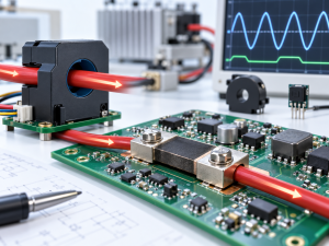
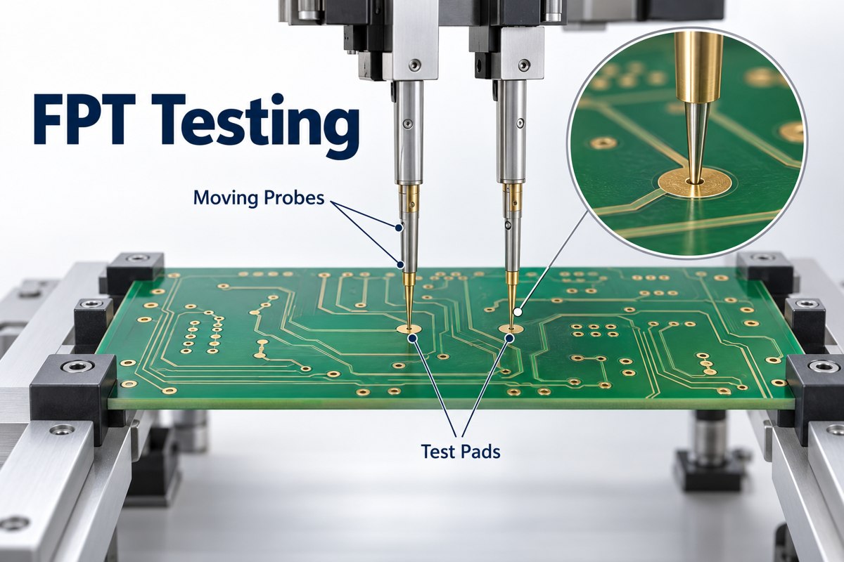
FPT Testing means flying probe testing in PCB manufacturing: software-controlled probes contact exposed conductors to measure electrical connections without a dedicated bed-of-nails test fixture. On a bare PCB, the main checks are continuity and isolation. On an assembled PCBA, suitably equipped systems can also measure components and detect selected assembly faults. The important distinction is what the test program actually covers, not simply whether a board has passed through a tester. FPT is useful for prototypes, frequent design revisions, and production where fixture investment is difficult to justify; it does not automatically replace powered functional testing.
Key Takeaways
- Bare-board FPT checks intended connections and separation between different nets; PCBA testing requires additional circuit and component information.
- A flying probe system avoids a dedicated bed-of-nails fixture, but still needs programming, alignment, board support, and reliable contact.
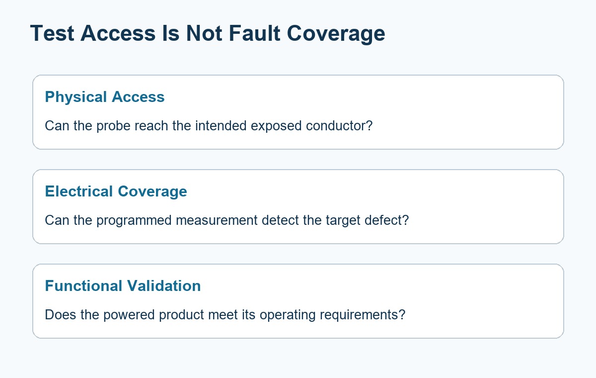
- Testing every board is not the same as detecting every possible fault. Ask which nets, components, and failure modes are covered.
- FPT versus ICT is a cost-and-throughput decision: compare setup cost, cycle time, design changes, and coverage for the actual product.
- Provide released design data and agreed electrical limits; keep inaccessible points and excluded tests visible in the test plan.
- At EBest Circuit, we offer bare-PCB flying probe testing and can coordinate PCB fabrication, assembly, and the inspection requirements of your project.
What Does FPT Testing Check on a PCB?
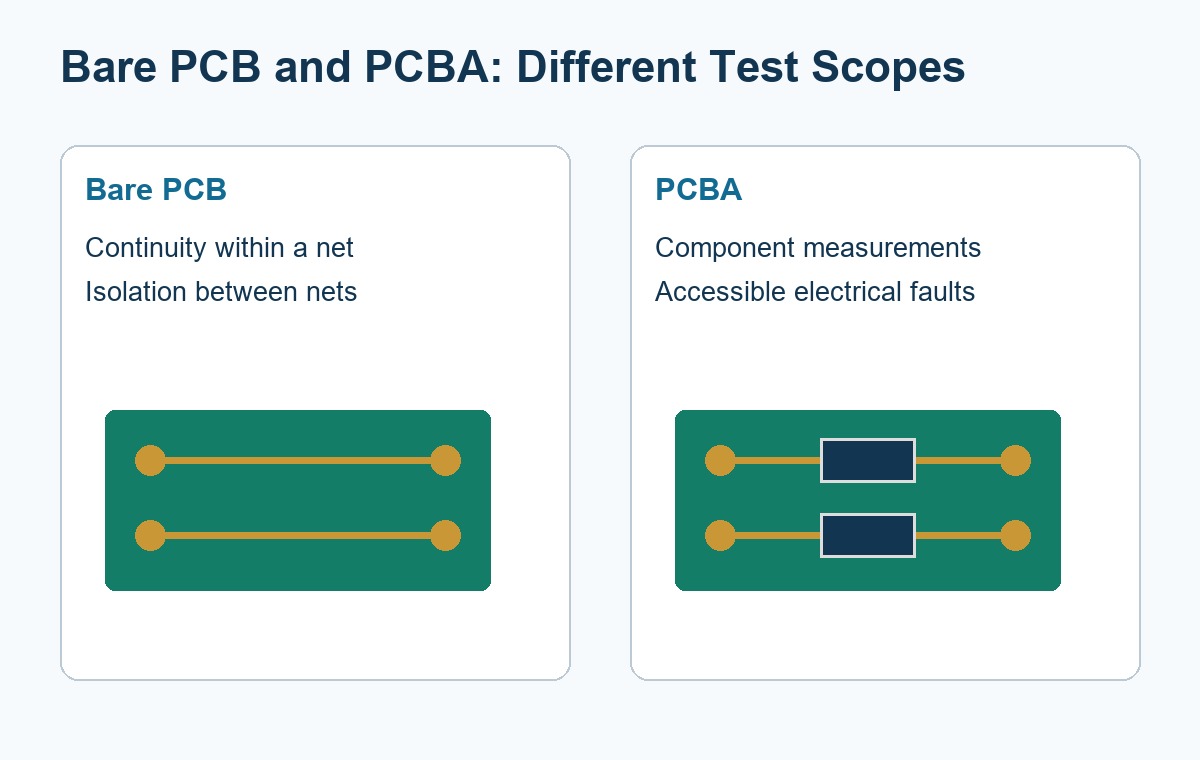
FPT checks whether conductors that should connect are connected and whether separate nets remain electrically isolated. A net is a group of points intended to share the same electrical connection.
| Test object | Main checks | Required reference |
| Bare PCB | Continuity, opens, shorts, isolation | Released netlist and board geometry |
| Assembled PCBA | Accessible connection faults and supported component measurements | CAD data, schematic, BOM, and validated test program |
| Powered product | Operating behavior, interfaces, and load response | Separate functional test specification |
At EBest Circuit, our PCB inspection capabilities include flying probe testing, universal electrical testing, AOI, and impedance testing. For a combined fabrication and PCB assembly order, we review the required checks at each stage rather than treating bare-board electrical acceptance as approval of the completed product.
Flying Probe Testing Explained: How Does It Work?
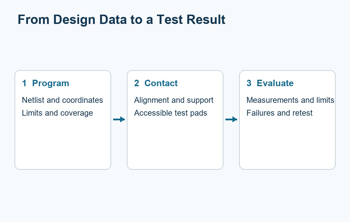
The tester moves probes to programmed coordinates, makes electrical contact, and compares measured values with the approved limits. The following sequence describes a typical test workflow, not one fixed machine configuration.
- Prepare the program. Import the released geometry and netlist; for assemblies, add component and circuit information. Define measurements and exclusions.
- Align and support the board. Locate fiducials or other registration features, check orientation, and support the panel so contact does not cause excessive movement.
- Make controlled contact. Move to accessible pads, vias, or other approved conductors. Component height and probe approach affect access.
- Measure and classify. Compare the result with the programmed threshold or range. Record a failure against an identifiable net, point, or component.
- Investigate and retest. Separate a real electrical defect from contact or programming trouble, repair only under the approved process, and retain the retest outcome.
Which Faults Can Flying Probes Detect?
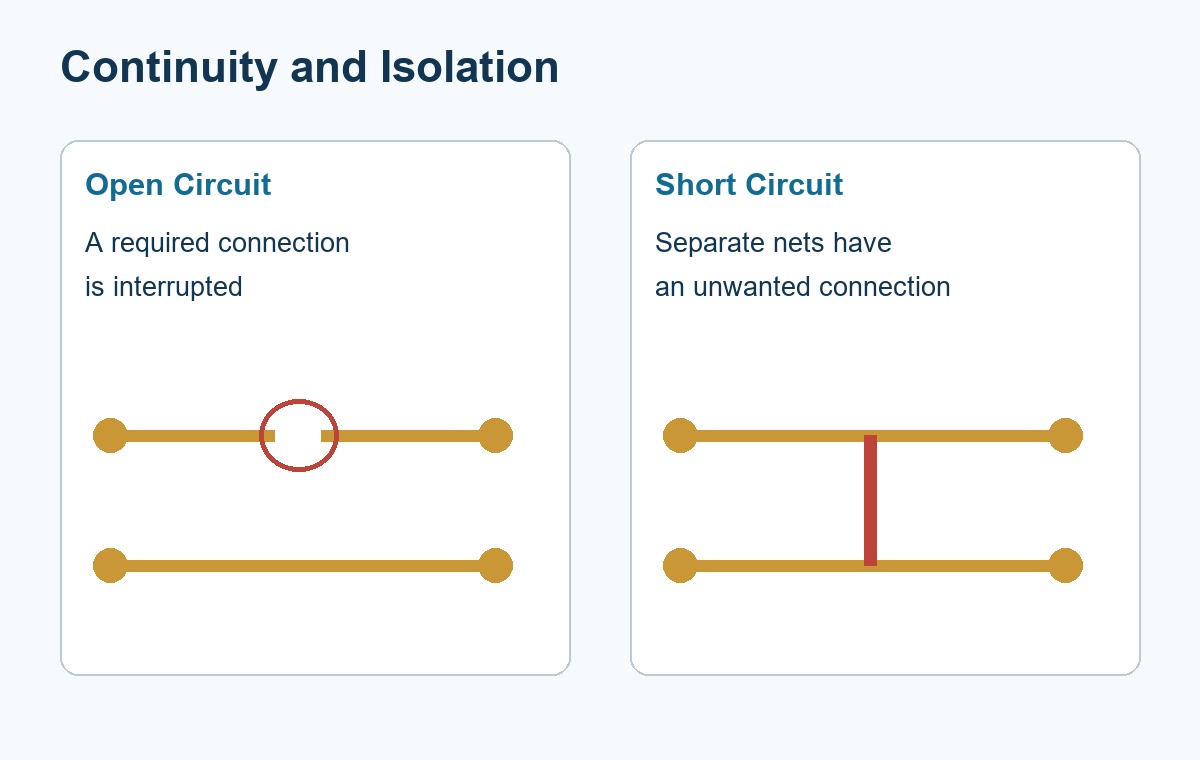
Flying probes can detect opens, unwanted connections, and supported out-of-range electrical measurements when the relevant circuit points are accessible and included in the program.
- Open connection: a broken trace or failed conductive path interrupts a required connection.
- Short circuit: two nets that should remain separate are unintentionally connected.
- Component-value error: assembly equipment may identify an incorrect resistance or capacitance when the surrounding circuit permits a meaningful measurement.
- Selected polarity or junction faults: appropriate measurement methods can check accessible semiconductor junctions; this is not a universal polarity check for every component.
Parallel paths matter. A resistor measured in circuit can appear lower than its standalone value because other paths conduct between the same test points. The program needs a suitable measurement strategy and limits; comparing every reading directly with the BOM nominal value can create false failures.
Flying Probe Testing vs ICT
Flying probe testing uses movable contacts; conventional fixture-based ICT uses a product-specific bed of nails to reach many test points through a fixed interface. FPT can perform in-circuit measurements, so the common comparison is really movable-probe access versus fixture-based access.
| Factor | Flying probe | Fixture-based ICT |
| Product-specific hardware | No dedicated bed of nails; support or interface hardware may still be needed | Dedicated fixture and interface |
| Design revisions | Usually handled through program and access updates | May require fixture modification as well as program changes |
| Cycle time | Probe travel and measurement sequence contribute to time | Fixed access often favors repetitive high-volume testing |
| Initial investment | Programming and validation without a full custom contact fixture | Fixture engineering, fabrication, programming, and validation |
| Selection basis | Changing designs, mixed products, required coverage and measured throughput | Stable designs, repeated volume, required coverage and measured throughput |
There is no universal quantity at which ICT becomes cheaper. Compare total setup cost plus quantity multiplied by test cost per board, including loading and retest. Modern flying probe systems can also serve production lines; a prototype-only rule would be too restrictive.
What Determines a Flying Probe Testing Machine’s Capability?
Probe access, supported measurement methods, board handling, and the validated program determine capability—not the number of probes alone. A flying probe testing machine for bare boards should not be assumed to provide the same assembly diagnostics as a PCBA tester.
- Access: contactable pad size, positioning accuracy, approach clearance, and one- or two-sided probing.
- Board handling: usable test area, component-height clearance, panel support, and loading method.
- Measurement resources: available resistance, capacitance, junction, isolation, or other test methods.
- Optional functions: powered measurements, programming, or additional inspection only where the installed system and project setup support them.
For example, SPEA describes its 4060S2 with four top-side probes and a bottom moving platform for additional test resources. That illustrates why machine configuration matters; it is not a statement that EBest Circuit operates that model or that its specifications apply to every test order.
How Should You Prepare a Board for FPT?
Provide exposed, reachable contact points and a consistent coordinate reference, then have the testing team review the layout before fabrication. “Fixtureless” does not mean the layout needs no design-for-test review.
- Identify test-point coordinates, net names, board side, and fiducials in the released data.
- Keep intended contact areas free of solder mask or conformal coating unless a qualified alternative method is agreed.
- Check probe approach around tall connectors, heatsinks, shields, and closely spaced components.
- Specify board thickness and panel format so clamping and support can be assessed.
- Confirm acceptable probe marks for contact fingers, wire-bonding areas, and other sensitive surfaces.
Do not copy a minimum test-pad diameter from an unrelated tester datasheet into your design rules. The practical limit depends on the equipment, probe tip, registration accuracy, board movement, and nearby obstacles. The useful output of a PCB design review is an approved access plan for your board.
What Files and Test Limits Should You Provide?
For a bare PCB, send the fabrication data and an independent released netlist where available; for PCBA, also provide the BOM, schematic, placement data, and required electrical tests.
- Bare-board package: Gerber or an agreed intelligent CAD format, drill data, fabrication drawing, and IPC-356 netlist where supported.
- Assembly package: BOM with reference designators, schematic, component coordinates and sides, assembly drawing, and relevant component data.
- Acceptance settings: continuity resistance limit in Ω, isolation resistance limit in MΩ, test voltage in V, and any special test conditions.
- Traceability: PCB revision, BOM revision, panel identification, and required lot or unit identification.
An independent design netlist helps expose a mismatch between the intended connections and the manufacturing artwork. A netlist generated only from that same artwork is less independent as a reference. Our PCB flying probe overview introduces the method; the acceptance settings above define how it should be applied to a specific order.
What Does an FPT Pass Result Not Prove?
An FPT pass shows that the programmed measurements met their limits; it does not prove full product function, every solder joint’s integrity, or long-term reliability.
- Hidden joints: reaching a connected net is not the same as individually verifying every BGA joint on that net.
- Mechanical quality: electrical continuity alone does not measure solder-joint strength or eliminate fatigue risk.
- Operating behavior: firmware, communication timing, RF performance, and full-load operation need appropriate additional tests.
- Untested paths: inaccessible points and omitted measurements remain outside demonstrated coverage.
Ask for a report that identifies the board revision, test-program revision, limits, tested quantity, failed locations, exclusions, and retest disposition. “100% tested” should state whether it means every delivered board was tested or a defined coverage metric. Those are different claims.
FAQ About FPT Testing
Can flying probes test multilayer PCBs?
Yes. Accessible endpoints can be used to check electrical paths that pass through internal layers and vias. The probes do not physically touch buried copper. Detection still depends on the netlist, available endpoints, and the measurements selected.
Can flexible circuits be tested?
Yes, with suitable handling and support. A flexible circuit can deflect under probe force, so the setup must hold it stable and maintain registration. Support tooling does not turn the process into a dedicated bed-of-nails test.
Should testing happen before conformal coating?
Normally, exposed-pad electrical testing is planned before coating, because coating can block reliable contact. If a later test is required, agree on masked test areas, connector access, or another qualified method rather than assuming probes can penetrate the coating safely.
Does flying probe testing damage a PCB?
Properly controlled probing is intended to test without unacceptable damage, but contact can leave witness marks. Sensitive finishes and functional contact surfaces need an agreed contact strategy and acceptance criteria; a blanket “no marks” promise is not appropriate.
Why can the same board fail once and pass on retest?
Poor contact, contamination, alignment error, movement, or an unstable measurement can cause intermittent results. An intermittent board defect is also possible. Investigate the cause and retain both outcomes instead of accepting the second result without explanation.
How Can EBest Circuit Support Your PCB Test Requirements?
We provide bare-PCB flying probe testing within our PCB manufacturing capabilities and coordinate assembly inspection and functional-test requirements for PCB/PCBA projects. When requesting flying probe testing services, tell us whether you need bare-board acceptance, assembly electrical diagnostics, or a complete product test plan.
Send your released board files, quantity, board revision, and required test limits to sales@bestpcbs.com. For assembled boards, include the BOM, schematic, and functional-test specification so we can review the scope and identify any additional setup before quoting.