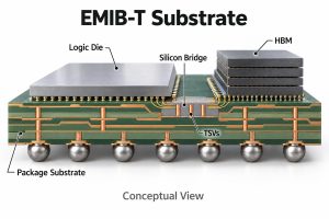
EMIB, or Embedded Multi-die Interconnect Bridge, is a 2.5D packaging technology that connects neighboring dies through small silicon bridges embedded inside the package substrate. Instead of placing an entire multi-die assembly on a large silicon interposer, EMIB concentrates fine-pitch routing only where high-bandwidth connections are required.
This localized architecture is well suited to chiplet processors, AI accelerators, HPC devices, FPGAs, and logic-plus-HBM packages. It combines the routing density of silicon at critical die interfaces with the larger routing area, power distribution, and mechanical support provided by an organic package substrate.
Key Takeaways
- EMIB stands for Embedded Multi-die Interconnect Bridge, a 2.5D packaging technology that places small silicon bridges inside the package substrate for high-density die-to-die connections.
- Unlike a large silicon interposer, EMIB uses silicon only at selected interfaces where fine-pitch routing is required.
- The silicon bridge connects adjacent logic dies, chiplets, or HBM through short, dense interconnects while the surrounding package substrate handles broader routing and power distribution.
- EMIB manufacturing combines silicon bridge fabrication with cavity formation, bridge embedding, substrate build-up, fine routing, die attach, and package testing.
- EMIB, EMIB-M, and EMIB-T share the localized bridge concept but add different electrical capabilities, including integrated capacitors or TSV-enabled vertical connections.
- EMIB and CoWoS-L both use localized silicon interconnect structures, although their surrounding routing media and overall package architectures differ.
What Is EMIB?
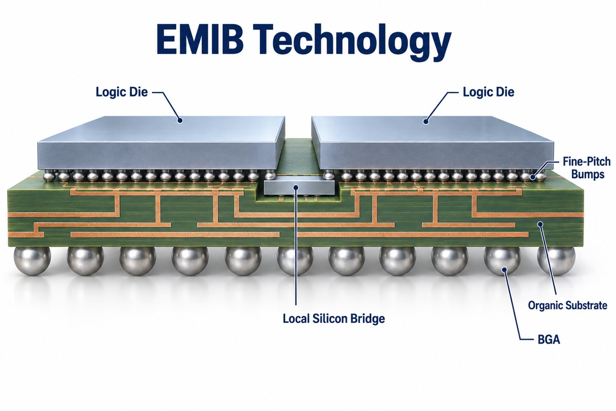
EMIB is a localized silicon-bridge packaging architecture that provides high-density electrical connections between adjacent dies. A small piece of silicon with fine metal routing is embedded in the package substrate beneath the edges of two neighboring dies.
Fine-pitch bumps connect both dies to this silicon bridge. Signals can then cross the die boundary through short, dense routing without requiring a large silicon interposer underneath the complete package.
A typical EMIB package can include:
- logic dies or compute chiplets;
- HBM stacks;
- one or more embedded silicon bridges;
- fine-pitch die-to-bridge connections;
- an organic package substrate;
- copper power and signal routing;
- BGA connections to the system PCB.
The bridge is used where routing density is highest. Lower-density signals, power, ground, and package-level connections can remain in the surrounding substrate, allowing different parts of the package to use interconnect structures suited to their actual electrical requirements.
What Is an EMIB Substrate?
An EMIB substrate is a package substrate containing one or more embedded silicon bridges beneath selected die interfaces. It still performs the normal functions of an advanced IC package substrate, but adds localized regions capable of much finer routing.
The main structures include:
| Structure | Main Function |
| Organic package substrate | Broad signal routing, power distribution, and mechanical support |
| Embedded silicon bridge | High-density die-to-die routing |
| Build-up layers | Connect the bridge to surrounding substrate routing |
| Fine-pitch bumps | Connect dies to the bridge |
| Copper vias and planes | Carry power, ground, and package-level signals |
| BGA solder balls | Connect the package to the system PCB |
The key feature is localization. Only the interfaces that need very high routing density use silicon, while the rest of the package can rely on organic build-up technology.
This is useful in heterogeneous packages because routing requirements are rarely uniform. A compute die may need thousands of closely spaced connections to HBM, while other interfaces can operate with much wider routing pitches.
How Does EMIB Work?
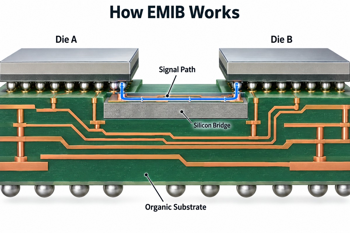
EMIB works by routing high-speed signals through an embedded silicon bridge positioned directly below the edges of neighboring dies. Fine-pitch bumps connect each die to the bridge, and the bridge’s metal layers carry signals across the gap.
The signal path can be simplified as:
- Die A → Fine-Pitch Bumps → Silicon Bridge
- Silicon Bridge → Fine-Pitch Bumps → Die B
This architecture is suitable for several high-bandwidth connections, including:
- logic-to-logic;
- compute-to-I/O;
- logic-to-HBM;
- accelerator-to-memory;
- chiplet-to-chiplet interfaces.
The surrounding organic substrate does not need to match the bridge’s routing density. It can handle broader signal paths, power distribution, and connections toward the BGA, which keeps the high-density silicon region focused on the die boundaries where it provides the greatest value.
Why Does EMIB Use a Local Silicon Bridge?
EMIB uses a local silicon bridge because high-density routing is usually required only at specific die interfaces rather than across the entire package. A localized bridge places silicon exactly where the fine-pitch interconnect is needed.
This architecture provides several practical benefits:
- silicon area is concentrated at critical interfaces;
- neighboring dies communicate through short electrical paths;
- organic routing remains available across most of the package;
- bridge placement can follow the actual chiplet floorplan;
- several bridges can be distributed across a large package;
- package size can grow without requiring one equally large silicon interposer.
For example, a package containing multiple compute chiplets and HBM stacks may need very dense routing only between each logic die and its neighboring memory. Local bridges allow those interfaces to use silicon-level routing while the rest of the substrate remains optimized for package-scale connections.
What Is the EMIB Process Flow?
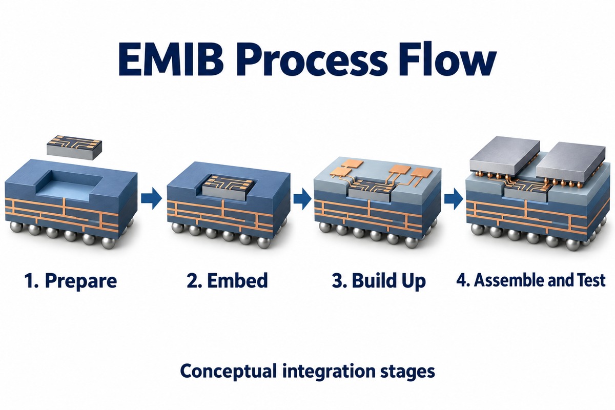
The EMIB process flow combines silicon bridge fabrication, substrate cavity preparation, bridge embedding, build-up routing, and final multi-die assembly. Exact production details depend on the package generation, but the general manufacturing sequence follows the same structure.
- Silicon bridge fabrication Fine metal routing is fabricated on the silicon bridge using semiconductor-compatible processing.
- Substrate cavity formation A recessed region is prepared at the location where the bridge will be embedded.
- Bridge placement The silicon bridge is accurately positioned inside the package substrate.
- Dielectric build-up Organic dielectric layers are formed around and above the embedded bridge.
- Copper routing formation Copper traces and vias connect the bridge region with the broader substrate routing.
- Fine-pitch interface preparation Pads and bump structures are prepared above the bridge for die attachment.
- Die attach Logic dies, chiplets, HBM, or other components are mounted on the substrate.
- Package assembly and test Underfill, mechanical reinforcement, electrical inspection, and reliability testing complete the package.
Bridge alignment is especially important because the embedded structure has to register with both the substrate routing below and the fine-pitch die connections above. Smaller interconnect pitches reduce the available margin for dimensional variation.
What Are the Main Advantages of EMIB?
The main advantage of EMIB is that it provides silicon-level routing density without requiring a package-wide silicon interposer. This makes the architecture attractive when only selected interfaces need extremely dense connections.
Key advantages include:
- High interconnect density: fine silicon routing supports wide die-to-die interfaces.
- Short signal paths: adjacent dies communicate through compact local bridges.
- Localized silicon usage: silicon is used mainly where its routing capability is required.
- Heterogeneous integration: logic, memory, I/O, and accelerator dies can share one package.
- Flexible floorplanning: bridge locations can follow chiplet placement.
- Package scalability: multiple bridge regions can be distributed across a larger package.
- Process-node flexibility: individual dies can use fabrication nodes suited to their functions.
This is particularly useful for chiplet architectures. Compute logic can use an advanced node, while I/O, analog, or supporting functions can use other processes without giving up high-bandwidth die-to-die communication.
What Are the Main EMIB Design and Manufacturing Challenges?
EMIB manufacturing must integrate fine-feature silicon structures into a much larger organic substrate while maintaining alignment, planarity, electrical performance, and long-term reliability.
The main challenges include:
- Bridge placement accuracy: the silicon bridge must align precisely with fine-pitch die interfaces.
- Substrate warpage: silicon, copper, dielectric, and molding materials expand differently during thermal cycling.
- Coplanarity: uneven surfaces can affect die attach and fine-pitch joint quality.
- Microbump reliability: small joints experience thermal and mechanical stress during assembly and operation.
- Signal integrity: impedance, crosstalk, return paths, and interconnect discontinuities require careful control.
- Thermal-mechanical stress: large logic dies and HBM stacks can create strong temperature gradients.
- Yield management: a late-stage defect may affect several expensive known-good dies in the same package.
These issues become more difficult as package size increases. Larger substrates have tighter requirements for dimensional stability because even small material movement can affect bridge registration and fine-pitch assembly across the package.
EMIB vs Silicon Interposer: What Is the Difference?
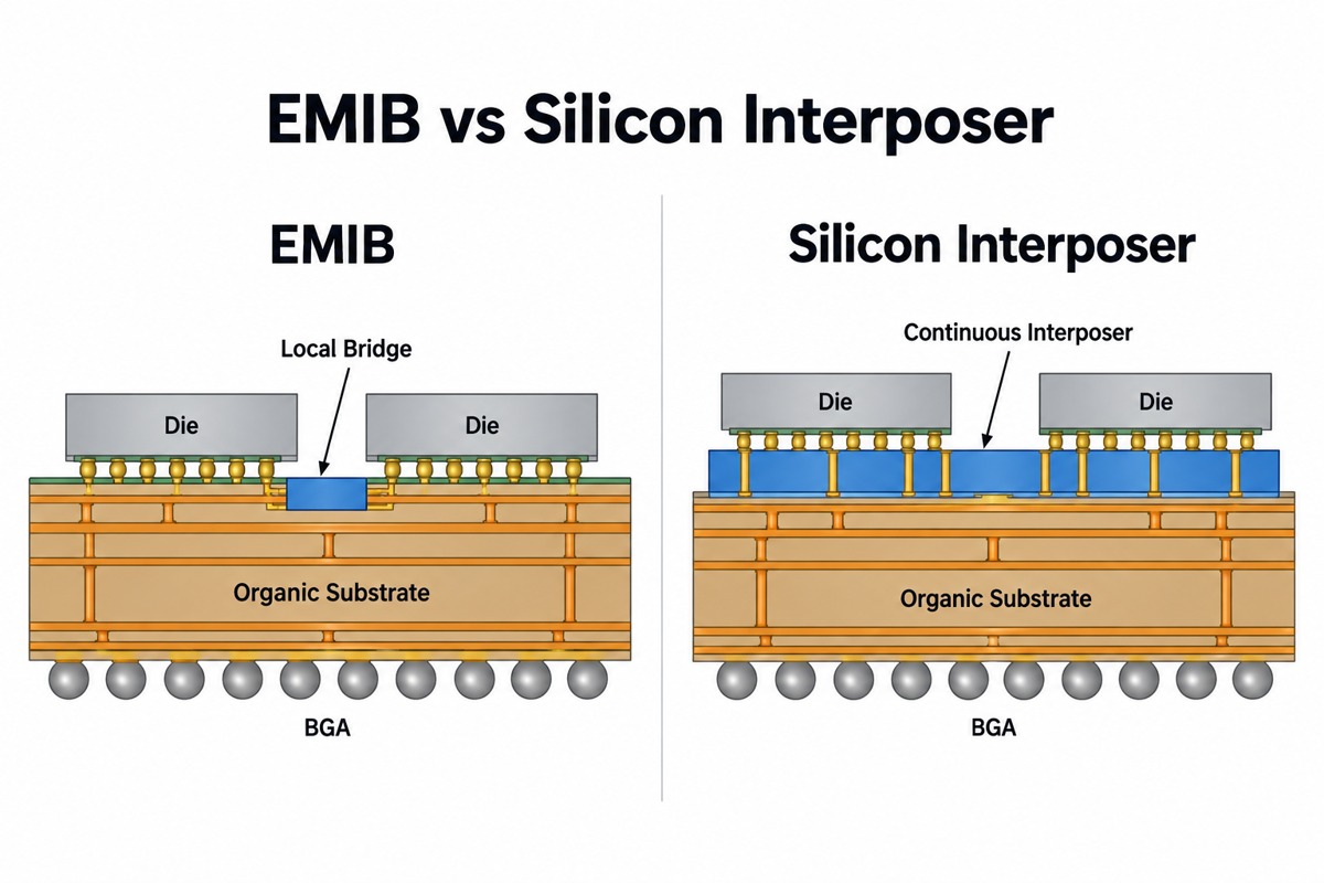
EMIB uses small localized silicon bridges, while a conventional silicon-interposer package uses a much larger continuous silicon routing layer beneath multiple dies. Both provide fine-pitch interconnection, but they distribute the high-density silicon very differently.
| Feature | EMIB | Silicon Interposer |
| Silicon routing area | Local bridge regions | Large continuous area |
| Position | Embedded in package substrate | Beneath multiple dies |
| Fine routing coverage | Selected die interfaces | Broad interposer area |
| Package-level routing | Mainly organic substrate | Interposer + substrate |
| Conventional bridge TSVs | Not required | Common in silicon interposers |
| Scaling approach | Add localized bridges | Increase interposer area |
A full silicon interposer is useful when dense routing is required across a broad die complex. EMIB is more localized, making it suitable when the highest routing density is concentrated along specific die boundaries.
The appropriate architecture depends on the package floorplan, number of dies, HBM placement, routing density, power distribution, thermal behavior, assembly requirements, and manufacturing economics.
EMIB vs CoWoS-L: How Do the Architectures Differ?
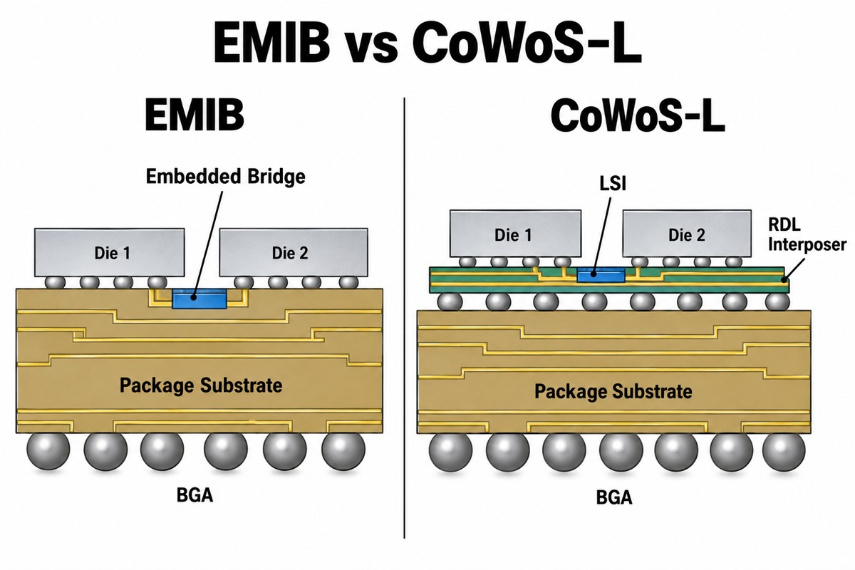
EMIB embeds localized silicon bridges directly inside the package substrate, while CoWoS-L uses local silicon interconnect structures within a broader RDL-based interposer architecture. Both use localized silicon for dense connections, but the surrounding routing structures are different.
| Feature | EMIB | CoWoS-L |
| Local silicon structure | Embedded silicon bridge | Local Silicon Interconnect |
| Surrounding routing medium | Package substrate | RDL interposer |
| Fine-pitch routing | Localized | Localized |
| HBM integration | Supported | Supported |
| Package scaling | Multiple bridge regions | Larger RDL interposer with local silicon |
| Broader routing | Organic build-up layers | RDL structure |
In an EMIB package, the organic substrate performs much of the broader routing around each silicon bridge. In CoWoS-L, the localized silicon structures are part of a larger redistribution-layer interposer system.
A practical comparison should consider more than the presence of a bridge. Engineers also need to evaluate:
- die and HBM placement;
- routing density;
- package dimensions;
- power distribution;
- warpage;
- thermal behavior;
- assembly flow;
- yield;
- overall package cost.
These architectural differences become increasingly important as AI and HPC packages integrate more compute silicon and memory within the same package footprint.
EMIB, EMIB-M and EMIB-T: What Is the Difference?
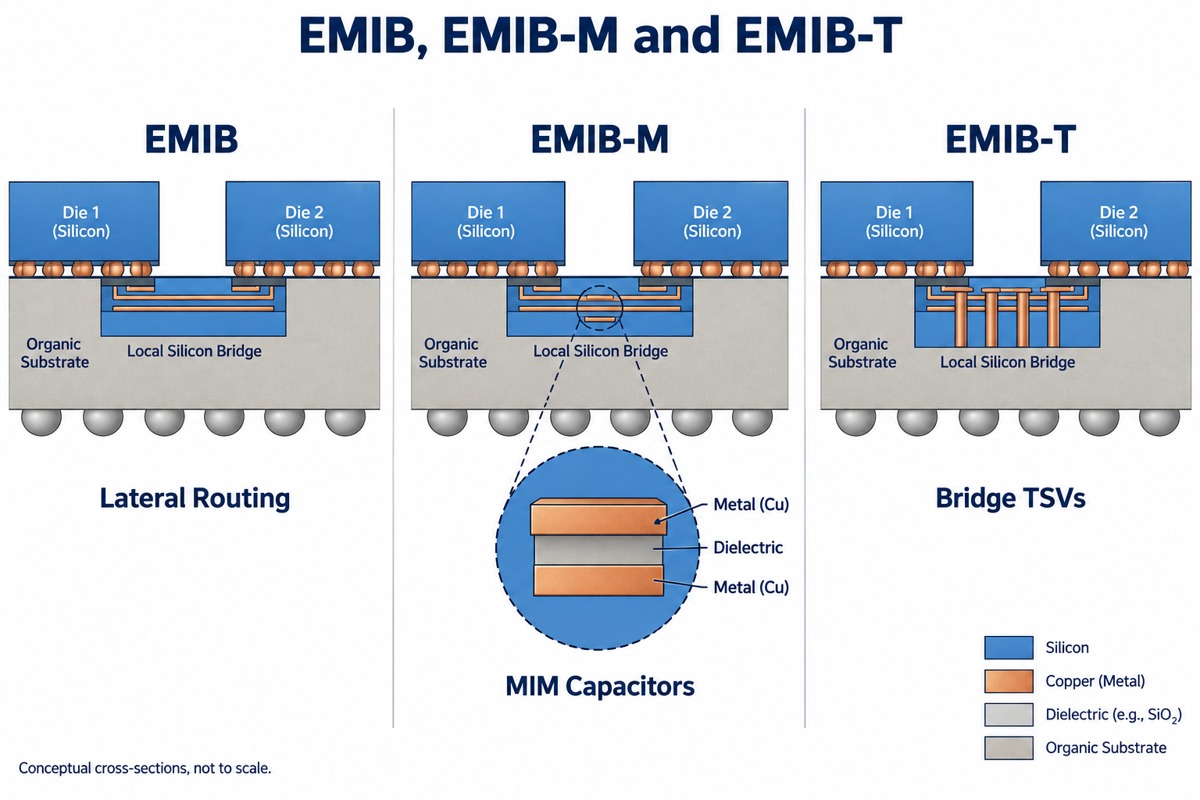
EMIB, EMIB-M, and EMIB-T share the same localized silicon-bridge concept, but the newer variants add specific electrical functions. Standard EMIB focuses mainly on lateral routing, while EMIB-M and EMIB-T expand the role of the bridge.
| Technology | Main Addition | Primary Function |
| EMIB | Local silicon bridge | Fine-pitch lateral die-to-die routing |
| EMIB-M | Integrated MIM capacitance | Local decoupling and power support |
| EMIB-T | TSVs through the bridge | Vertical electrical and power paths |
EMIB-M integrates metal-insulator-metal capacitance close to the dies, which can support local power delivery and decoupling. EMIB-T adds through-silicon vias, allowing selected electrical paths to move vertically through the bridge.
The distinction is especially relevant for newer AI and HBM packages. As current demand increases, the bridge can evolve from a primarily signal-routing structure into a more active part of the package power-delivery architecture.
How Does EMIB Connect Chiplets, HBM and UCIe?
EMIB provides the physical high-density connection between neighboring chiplets or between logic and HBM. The silicon bridge carries the electrical signals, while standards such as UCIe define how compatible chiplets communicate at the interface level.
Typical EMIB connections include:
- compute die to compute die;
- compute die to I/O die;
- compute die to HBM;
- accelerator to accelerator;
- UCIe-compatible chiplet links.
HBM is a strong use case because its wide interface benefits from short routing distances and high connection density. Chiplet interfaces have similar requirements when several dies need to exchange large volumes of data within the same package.
UCIe and EMIB therefore address different layers of the connection. UCIe defines the die-to-die interface framework, while EMIB can provide the physical package interconnect that carries those signals between adjacent dies.
Where Is EMIB Used in AI and HPC Packaging?
EMIB is used in advanced packages where multiple high-performance dies, memory stacks, or specialized chiplets require dense local interconnections. These applications increasingly depend on package-level bandwidth as much as on transistor performance.
Common application areas include:
- AI training accelerators;
- AI inference processors;
- HPC processors;
- data-center CPUs;
- FPGAs;
- multi-die GPUs and XPUs;
- chiplet-based compute platforms;
- logic-plus-HBM packages.
Heterogeneous integration also allows each die to use a manufacturing process suited to its function. Compute cores can use an advanced node, while I/O, analog, or supporting logic can remain on nodes better suited to cost, voltage, or interface requirements.
This approach helps designers scale system performance without increasing every function inside one extremely large monolithic die.
Can EMIB Use a Glass-Core Substrate?
EMIB can potentially be integrated with glass-core substrate platforms as advanced packages move toward larger dimensions and tighter registration requirements. Conventional EMIB, however, should still be understood as an embedded silicon-bridge architecture rather than a technology defined by glass substrates.
Glass-core substrates are being explored because they can offer useful properties for very large advanced packages:
- improved dimensional stability;
- lower warpage potential;
- support for larger package formats;
- finer routing capability;
- stable electrical characteristics;
- support for dense vertical and lateral interconnects.
Glass also introduces manufacturing challenges, including via formation, metallization, substrate handling, bonding, and integration with organic build-up layers. These processes must meet the same reliability and production requirements expected from established package-substrate platforms.
For future EMIB scaling, improved substrate stability could become increasingly valuable as packages integrate more silicon bridges, chiplets, and HBM stacks while maintaining tight alignment across a larger area.
EMIB FAQs
1. What does EMIB stand for?
EMIB stands for Embedded Multi-die Interconnect Bridge. It uses small silicon bridges embedded inside a package substrate to create fine-pitch connections between neighboring dies.
2. Is EMIB a 2.5D packaging technology?
Yes. EMIB is generally classified as a 2.5D heterogeneous integration technology because multiple dies are placed side by side and connected through localized high-density silicon interconnects.
3. Does EMIB use TSVs?
Conventional EMIB bridges do not require TSVs for their primary lateral die-to-die connection. EMIB-T is the variant that adds TSVs through the bridge for vertical electrical and power paths.
4. What is an EMIB substrate?
An EMIB substrate is a package substrate containing embedded silicon bridges beneath selected die interfaces. The bridges handle fine-pitch routing, while the surrounding substrate carries broader signals, power, and ground.
5. What is the difference between EMIB and CoWoS?
EMIB places localized silicon bridges directly inside the package substrate. CoWoS is an interposer-based packaging family, while CoWoS-L combines localized silicon interconnects with a broader RDL interposer structure.
6. What is the difference between EMIB and EMIB-T?
Standard EMIB mainly provides lateral die-to-die routing through an embedded silicon bridge. EMIB-T adds TSVs through that bridge, creating vertical electrical paths that can support more demanding power-delivery requirements.