Positive vs negative photoresist differs in what happens to the exposed coating during development. In a positive resist, the exposed area becomes soluble and is removed. In a negative resist, exposure hardens or crosslinks the material, so the exposed area remains.
That reversal changes mask polarity, but tone alone does not decide which resist will print the smallest feature or survive the next process. Choose by required line and space, film thickness, exposure system, substrate, developer, etching or plating chemistry, and stripping method.
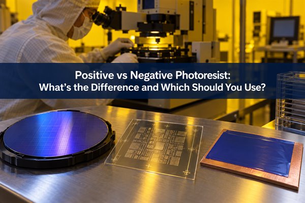
What Are Positive and Negative Photoresists?
Positive and negative are imaging tones: they identify which part of a light-sensitive coating remains after development. The terms do not indicate electrical polarity, film color, or product quality.
In a positive photoresist, the developer removes the areas that received enough exposure. The unexposed coating stays on the substrate and protects the material below. This creates a resist image that follows the dark regions of the photomask.
In a negative photoresist, exposure makes the illuminated areas resistant to the developer. The unexposed coating is washed away, so the remaining resist follows the clear regions of the mask. That image may act as an etch barrier, a plating mold, a temporary process film, or a permanent microstructure, depending on the product.
How Do Positive and Negative Photoresists Work?
Both materials convert an optical image into a patterned coating, but exposure changes their solubility in opposite directions. The full imaging sequence is coat or laminate, expose through a mask or direct-imaging system, and develop.
Positive resist chemistry is formulated so that sufficient exposure makes the illuminated polymer easier for the specified developer to dissolve. Development therefore clears the exposed regions and leaves the unexposed film. The printed edge depends on how sharply the chemistry changes from insoluble to soluble across the exposure boundary.
Negative resist chemistry polymerizes, crosslinks, or otherwise hardens where it receives sufficient light. Development removes the unexposed regions and leaves the exposed network. Crosslink density affects sidewall shape, adhesion, chemical resistance, and how readily the film can be stripped later.
Exposure dose must match the resist thickness and light source. Too little energy may leave a positive resist incompletely cleared or a negative resist insufficiently crosslinked. Excess energy can widen or narrow the printed feature by moving the effective image boundary.
Positive vs Negative Photoresist: What Are the Main Differences?
The central difference is simple: exposed positive resist is removed, while exposed negative resist remains. This positive vs negative photoresist comparison shows how that reversal affects the image and the processes each tone commonly serves.
| Property | Positive Resist | Negative Resist |
|---|---|---|
| Exposed area | Removed | Remains |
| Unexposed area | Remains | Removed |
| Image formation | Exposure opens the coating | Exposure hardens the coating |
| Fine features | Often favored for high-resolution thin-film imaging | Capable when the material and process are optimized |
| Film thickness | Common in thinner coatings | Widely available as thick liquid or dry film |
| Adhesion | Controlled by formulation and surface preparation | Often strong after crosslinking |
| Typical uses | Semiconductors, microfabrication, selected PCB processes | PCB dry film, pattern plating, tenting, thick microstructures |
| Stripping | Often easier with the specified remover | May require a stronger or tightly controlled strip process |
How Does Photoresist Type Affect Mask Polarity?
The same clear mask area produces opposite developed results. A clear area lets light reach the resist; whether that location opens or stays protected depends on the resist tone.
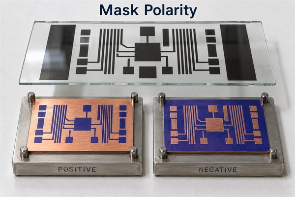
- Positive resist: A clear mask area exposes the resist; the developer removes that coating and opens the substrate at the same location.
- Negative resist: A clear mask area exposes and hardens the resist, so the substrate remains protected at the same location.
Start with the final surface that must be open for etching, plating, deposition, or another operation. Trace that area backward through development and exposure to determine whether it should be clear or opaque on the mask. If a process changes from positive to negative tone, the image logic normally has to be inverted; reusing the old artwork can reverse protected and open areas.
Which Photoresist Offers Better Resolution and Fine-Line Performance?
Positive photoresist is often associated with finer imaging, but resist tone does not set the minimum feature size by itself. A qualified negative material can outperform a poorly matched positive process, especially when the film, exposure tool, developer, and substrate preparation were developed as one system.
Positive resists can produce steep profiles because the exposed material dissolves rather than forming a crosslinked network that may swell during development. This behavior is useful in thin-film semiconductor and microfabrication processes. It does not mean every positive formulation is suitable for every wavelength, thickness, or substrate.
For an actual line-and-space target, compare these inputs:
- Resist thickness: Thicker films are harder to expose uniformly through their depth and can reduce aspect-ratio margin.
- Exposure wavelength and dose: The resist must absorb and react correctly at the tool’s wavelength, with enough latitude to hold the intended edge.
- Imaging geometry: Mask contact, collimation, direct-imaging focus, registration, and scattered light alter the printed feature.
- Development: Developer type, concentration, temperature, spray pressure, and dwell time affect clearing, swelling, and sidewall loss.
- Substrate condition: Surface roughness, oxide, contamination, and adhesion treatment change both image integrity and downstream yield.
Use the supplier’s resolution data only when its test thickness, exposure method, and process conditions are comparable to yours. For PCB work, the finished copper line after etching or plating matters more than the resist image alone.
How Do Positive and Negative Photoresists Compare in Thickness, Adhesion, and Durability?
Negative resists are often selected when the patterned film must be thick, mechanically robust, or resistant to prolonged chemical processing. Exposure builds a crosslinked structure that can hold tall features, bridge holes in a tenting process, or remain intact during plating.
Positive resists are widely used as thinner liquid coatings where clean development and fine profile control are priorities. Their adhesion and chemical endurance still depend on the formulation, bake sequence, surface preparation, and downstream chemistry. A thin positive film may be entirely suitable for a short etch but poorly matched to a long plating cycle.
- For thick films: Check whether the resist can be exposed through its full depth without a weak base or distorted sidewall.
- For adhesion: Match the resist to copper, silicon, glass, ceramic, or the actual substrate, then verify cleaning and bake conditions.
- For chemical durability: Compare the specified etchant, plating bath, cleaning steps, temperature, and dwell time with the material data.
- For stripping: Confirm that the hardened image can be removed without attacking the plated metal, substrate, or permanent coating that must remain.
Where Are Positive and Negative Photoresists Commonly Used?
Positive resists are common in fine-pattern thin-film work, while negative resists are common where the image must be thick or durable.
Positive photoresist applications include semiconductor lithography, microfabrication, lift-off processes using a suitable profile, photomask production, presensitized prototype PCBs, and selected liquid-resist PCB processes. These applications often value clean feature definition and predictable removal of the exposed region.
Negative photoresist applications include PCB dry-film imaging, pattern plating, hole tenting, thick electroforming molds, MEMS structures, and permanent epoxy-based features such as those made with SU-8. These processes often need film strength, thickness, adhesion, or resistance to later chemistry.
The same application category can use either tone when materials and equipment differ. If the existing line already meets the finished feature and reliability target, changing tone means reworking the mask logic, developer, exposure window, and stripping route.
Which Photoresist Is Commonly Used in PCB Manufacturing?
Negative-working dry film is widely used for commercial PCB imaging because it laminates uniformly, can tent selected holes, and forms a durable image for etching or pattern plating. Direct imaging and phototool exposure can both be used when the film is designed for the relevant wavelength and process.

Positive photoresist also has a place in PCB production. Positive presensitized boards are familiar in prototype and educational work, and positive liquid resists may be used in specialized or established imaging lines. A shop may also use different resist systems for inner layers, outer-layer pattern plating, solder mask, or non-PCB microfabrication, so “PCB photoresist” is not one universal chemistry.
For a PCB order, the customer usually does not need to prescribe resist tone. The useful inputs are finished copper thickness, minimum line and space, annular-ring and registration requirements, via structure, plating build, and surface finish. The fabricator can then choose a qualified imaging route that meets the finished-board drawing.
How Do Etching and Plating Requirements Affect Photoresist Selection?
Etching and pattern plating load the resist in different ways, so the downstream operation can decide which product is suitable even when both tones can print the artwork.
For an etch resist, the film must adhere through cleaning and etchant exposure, protect the copper or substrate without pinholes, and preserve the intended edge as material is removed beside it. Film thickness, sidewall shape, etchant resistance, and stripping after etch all affect the finished line width.
For pattern plating, the developed openings act as a mold. The resist must tolerate the plating chemistry and current distribution, remain bonded during the cycle, and provide enough thickness for the plated build without excessive mushrooming over the resist edge. Hole tenting or selective openings may further favor a robust dry film.
Specify the finished feature and downstream chemistry first. Then compare resist compatibility, required thickness, opening profile, adhesion, maximum process time, and removal method. This prevents a material that images cleanly from failing later in the line.
How Should You Choose Between Positive and Negative Photoresist?
Choose the resist that can produce the required finished feature within your existing exposure, development, and downstream process. Tone is one input; the qualified material system is the decision.
- Consider positive resist for a thin-film process that prioritizes fine feature definition, uses a compatible positive-tone mask, and already has controlled coating, exposure, development, and stripping conditions.
- Consider negative resist when the process needs a thicker or tougher image, dry-film lamination, hole tenting, pattern plating, prolonged chemical resistance, or a permanent crosslinked structure.
- Keep the existing qualified tone when it already meets the finished geometry and reliability requirement. Changing tone also changes mask logic, process chemistry, exposure latitude, and verification work.
Make the decision from measurable requirements: minimum line and space, resist thickness, substrate topography, exposure wavelength, available dose window, developer, etchant or plating bath, stripping limit, throughput, and defect tolerance. If two candidates remain, compare them on the actual substrate at the intended thickness and judge the developed image and finished feature, not the brochure category.
What Should You Check Before Selecting a Photoresist Material?
A tone choice becomes a usable material choice only when the product matches the equipment, substrate, chemistry, and finished feature. Check the following items on the current technical data sheet and process specification:
- Tone and format: Positive or negative; liquid, electrodeposited, or dry film; temporary or permanent.
- Coating thickness: Nominal and working range after coating, lamination, bake, exposure, and development.
- Exposure compatibility: Supported wavelength, recommended dose range, photospeed, and the capability of the mask aligner or direct-imaging tool.
- Development: Developer chemistry, concentration, temperature, time, rinse, and the observable clearing endpoint.
- Thermal steps: Soft bake, post-exposure bake, hard bake, and allowable substrate temperature.
- Substrate and adhesion: Approved surface materials, cleaning method, roughness, adhesion promoter, and topography limits.
- Downstream resistance: Compatibility with the actual etchant, plating bath, cleaner, solvent, and process duration.
- Stripping: Specified remover, temperature, time, residue risk, and compatibility with the finished metal or device.
- Storage and handling: Shelf life, refrigeration or humidity limits, yellow-room requirements, and equilibration before use.
Before releasing a full wafer lot or PCB panel, expose and develop a representative coupon using the intended thickness, substrate, artwork, and equipment. Inspect clearing, feature width, sidewalls, adhesion, and the result after the relevant etch or plating step. Freeze the production settings only after the coupon meets the finished-feature requirement.
FAQs About Positive vs Negative Photoresist
Q1: Is positive or negative photoresist better?
A1: Neither tone is better for every process. Positive resist is often chosen for thin, fine-feature imaging; negative resist is often chosen for thicker, durable films. The correct material must match the exposure tool, substrate, developer, downstream chemistry, and finished geometry.
Q2: Which photoresist is better for fine features?
A2: Positive resist is common in high-resolution thin-film lithography, but a modern negative resist can also resolve fine features. Compare data and test results at the required thickness and wavelength rather than selecting by tone alone.
Q3: Is PCB dry film photoresist positive or negative?
A3: Most common PCB imaging dry films are negative-working: exposed areas polymerize and remain after development. Confirm the exact product because specialized materials may use a different chemistry.
Q4: Is SU-8 a positive or negative photoresist?
A4: Standard SU-8 is an epoxy-based negative photoresist. Exposed regions crosslink and remain, which makes the material useful for thick, high-aspect-ratio and permanent microstructures.
Q5: Do positive and negative photoresists use the same developer?
A5: Not necessarily. Developer chemistry is product-specific; some systems are aqueous, while others use organic solvents or proprietary formulations. Use the developer and concentration stated for the exact resist.
Q6: Do you need to invert the mask when changing photoresist type?
A6: Usually yes, if the final protected and open areas must remain the same. Positive and negative tones respond oppositely under the same clear mask area, so confirm the mask polarity with a small exposure before production.
Q7: Can negative photoresist achieve fine lines?
A7: Yes. Fine-line performance depends on the specific material, film thickness, exposure optics, dose, development, surface condition, and the following etch or plating process. Negative-working dry films are used for fine PCB imaging when the complete process is qualified.
Q8: Which photoresist is easier to strip?
A8: Positive resists are often easier to remove because they do not form the same heavily crosslinked network, but removal still depends on the formulation and bake history. Check that the specified stripper will not damage the substrate or plated metal.
Q9: Can positive photoresist be used for PCB manufacturing?
A9: Yes. Positive presensitized boards and selected liquid-resist processes are used in PCB prototyping and specialized production. Commercial volume fabrication commonly uses negative dry film, but equipment and qualified process capability decide the actual route.
Q10: Why is negative dry film common in PCB fabrication?
A10: It can be laminated at a controlled thickness and forms a strong image that suits tenting, etching, and pattern plating. It also integrates well with established phototool and direct-imaging lines.
Positive photoresist removes exposed regions during development, while negative photoresist retains them. That difference changes mask polarity, but it does not by itself determine resolution or manufacturability. Film thickness, exposure conditions, adhesion, downstream chemistry, and stripping requirements decide whether a specific material fits the process.
For PCB production, judge the imaging process by whether it can repeatedly achieve the required line width, spacing, copper thickness, plating structure, and finished-board tolerances. Send your Gerber files, stackup, copper weight, minimum line and space, quantity, target delivery date, and any plating or inspection requirements to sales@bestpcbs.com for a manufacturability review and quotation.