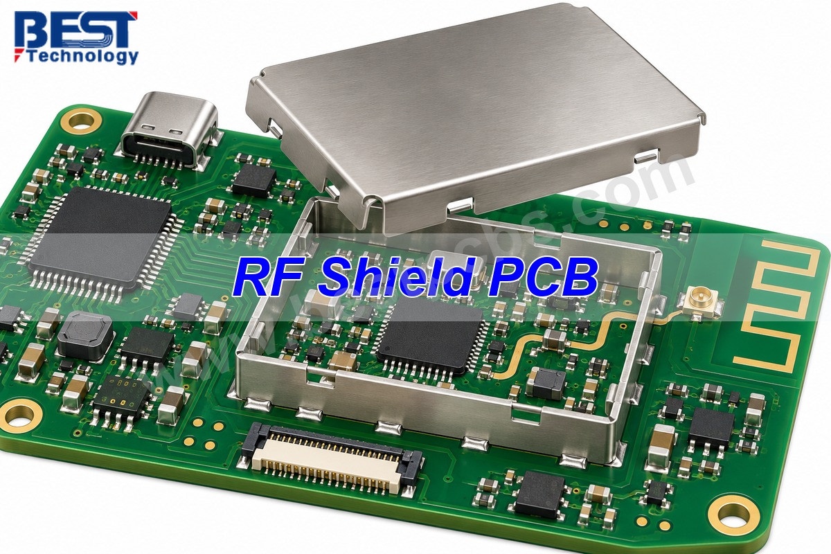
An RF shield PCB uses a conductive metal cover over selected components to reduce unwanted radio-frequency interference. The cover connects to the PCB ground system and helps keep noise from entering sensitive circuits or escaping from noisy sections of the board.
In a wireless receiver, shielding can separate a weak-signal circuit from nearby digital electronics. On a compact control board, it can contain emissions from a local noise source. The right shield must fit the circuit, provide a suitable ground connection, and leave the access needed for assembly or repair.
At EBest Circuit (Best Technology), we provide PCB fabrication, component sourcing, and assembly for prototype and production projects. Our PCB assembly services include SMT, through-hole, and mixed assemblies, allowing customers to source the board and its assembly through the same manufacturing partner.
Key Takeaways
- RF shield cans reduce radiated interference around selected circuits, while noise traveling through power and signal connections still requires attention to those paths.
- PCB designs that already meet their functional and emissions requirements may not need an additional metal shield.
- A 2-piece frame-and-lid design allows access to components without desoldering the frame.
- Shield material selection must account for solderability, surface finish, mechanical strength, and the frequencies involved.
- Internal height, component tolerances, and the installed mounting position determine whether a shield clears the parts underneath.
- Short, distributed connections to the PCB ground plane help the shield work at RF frequencies.
- Standard shield sizes can avoid custom tooling, while installation and future access also affect the total cost.
What Is an RF Shield on a PCB?
An RF shield on a PCB is a conductive enclosure that covers a specific circuit area to reduce electromagnetic coupling. Manufacturers also call it a shield can, screening can, or board-level shield. It usually has a metal top and sidewalls, with the PCB ground structure forming the lower part of the shielded region.
The metal reflects and absorbs part of the electromagnetic energy that reaches it. Its effectiveness also depends on the seams, openings, and connections around the enclosure. This explains why a well-fitted cover needs a suitable PCB layout underneath rather than simply sitting above the components.
Common applications include:
- Wireless receivers: Shielding helps protect low-level received signals from noise generated elsewhere on the board.
- RF modules: Local enclosures separate oscillators, amplifiers, and other circuit sections that could interfere with each other.
- Mixed-signal electronics: A shield can isolate sensitive analog circuitry from nearby processors and digital clocks.
- Compact industrial controllers: Closely packed power, communication, and measurement circuits may need local shielding where physical separation is limited.
RF shielding describes an interference-control feature, not a particular PCB laminate. Both conventional FR-4 boards and boards using specialized high-frequency materials can carry metal shields.
Is RF Shielding Necessary?
Not every PCB needs RF shielding. A metal shield becomes useful when unwanted radiated coupling prevents the circuit from working correctly or contributes to emissions that the product must reduce.
If the board operates reliably and meets its emissions and immunity requirements with its existing layout and enclosure, adding a shield may provide little benefit. It also occupies board space, increases component cost, and can make servicing harder.
The interference path determines whether shielding is the right solution. Noise carried into an amplifier through its supply rail needs attention to filtering, decoupling, or the supply layout. A cover over the amplifier may do little to stop that conducted noise. Conversely, noise coupling through the space between adjacent circuit sections is a situation where a local shield can help.
Some products already have a conductive enclosure that provides sufficient protection from external fields. They may still need internal shields if noisy and sensitive circuits interfere with each other inside that enclosure.
When Does a PCB Need RF Shielding?
PCBs benefit from RF shielding when sensitive circuitry sits close to a radiating noise source and the available layout cannot provide enough isolation.
Typical situations include:
- Receiver sensitivity falls when a processor runs. Digital clocks and their harmonics can couple into a nearby receiver, making weak signals harder to detect.
- A switching regulator sits beside an analog front end. Fast switching edges can disturb low-level measurements when separation and routing options are limited.
- Multiple RF sections share a small board. Oscillators, transmit paths, and receive paths may need separate shielded regions to limit unwanted coupling.
- A concentrated circuit area produces unwanted emissions. Shielding that area can contain part of the radiated energy without enclosing the entire PCB in a separate metal housing.
- External RF signals disturb a measurement circuit. Local protection can help when sensitive input stages remain exposed inside a plastic enclosure.
The shield can surround the noise source, the sensitive circuit, or separate compartments containing each. Covering the source may protect several neighboring circuits at once; covering only the sensitive section can use less board area.
These symptoms help identify where shielding may be useful, but the circuit layout still determines the enclosure boundary. A shield that leaves a noisy trace crossing into the protected area can miss the path causing the problem.
1-Piece vs 2-Piece PCB Shielding Cans: Which Should You Choose?
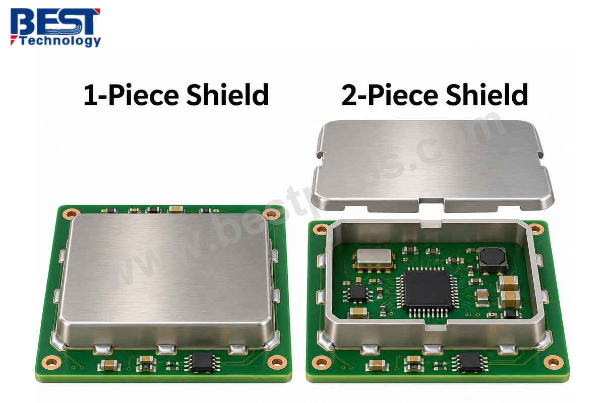
For components that need testing, adjustment, or repair after assembly, a 2-piece shield usually provides easier access. Directly soldered 1-piece shields suit circuits that rarely need access and can use a simpler enclosure.
| Selection factor | Directly soldered 1-piece shield | 2-piece frame and lid |
|---|---|---|
| Construction | Top and sidewalls form a single cover | Separate frame remains on the PCB beneath a removable lid |
| Component access | Usually requires desoldering the shield | Lid can be removed without desoldering the frame |
| Assembly | Cover attaches directly to the board | Frame attaches first; lid fits afterward |
| Maintenance | Less convenient for repeated access | Better suited to accessible test or repair areas |
| Main trade-off | Simpler construction, harder access | Additional part and lid-to-frame contact interface |
The distinction is not absolute: a 1-piece can held by PCB-mounted clips can also be removable. For a PCB RF shield can, both the cover structure and its mounting method determine access.
Multi-compartment shields add internal walls to separate neighboring circuit blocks. They can be useful when a transmitter and receiver need isolation within a shared footprint, but those walls also need appropriate contact with the PCB ground structure.
Which Materials Are Used for PCB RF Shields?
PCB RF shields commonly use nickel silver, tin-plated steel, and copper alloys; aluminum is another option where its attachment method suits the assembly. The choice depends on electrical performance, forming requirements, corrosion protection, and how the shield connects to the board.
For soldered shields, the surface finish matters as much as the base metal because the joint must wet properly during assembly.
| Material | Useful characteristics | Selection consideration |
|---|---|---|
| Nickel silver | Copper-based alloy with useful stiffness, formability, and corrosion resistance | Common in small shield cans; the name does not mean it contains silver |
| Tin-plated steel | Mechanical strength with a solderable tin surface | Plating condition and forming details affect the finished part |
| Copper and copper alloys | High conductivity and a range of forming properties | Temper and finish influence stiffness, oxidation, and solderability |
| Aluminum | Low weight and good electrical conductivity | Its oxide layer makes conventional PCB soldering difficult, so attachment needs a suitable mechanical or specialized solution |
There is no single best RF shielding material for every board. A soft, highly conductive metal may need more support than a stiffer alloy, while a mechanically convenient material may require plating for the intended soldering process.
Thickness also affects forming and rigidity. For miniature cans, a thinner wall saves space but can be easier to deform during handling. Increasing thickness does not automatically solve leakage through a poor lid seam or an open board connection, so wall thickness should not be the only specification used to compare shields.
How Are RF Shields Mounted on a PCB?
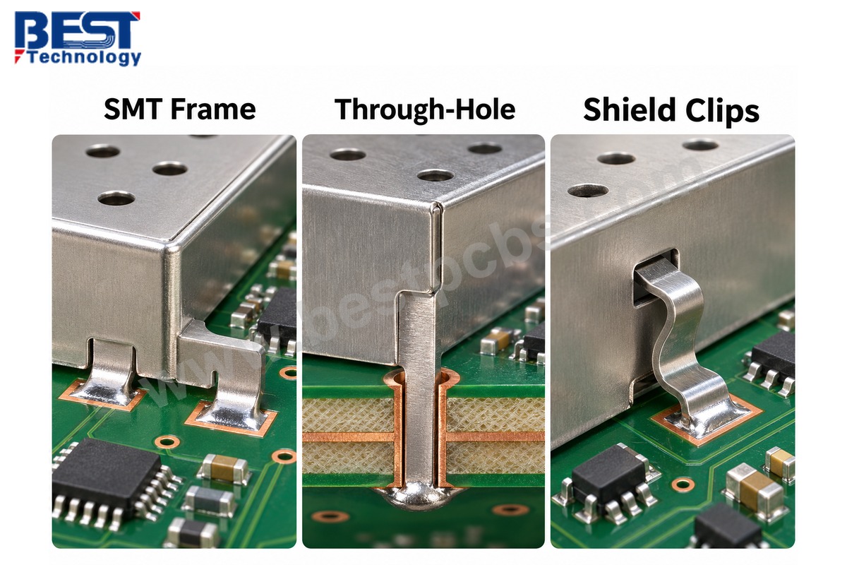
RF shields attach to a PCB through surface-mount solder joints, through-hole tabs, or retention clips. The selected shield’s footprint and installation method must match the board layout and assembly process.
| Mounting method | How it attaches | Where it fits |
|---|---|---|
| SMT frame or can | Solderable edges or feet connect to surface pads | Assemblies designed around reflow soldering |
| Through-hole tabs | Tabs enter plated holes or slots and are soldered | Designs that allocate board space for tab locations and solder access |
| SMT clips with a removable can | Clips solder to the PCB; the can presses into them | Assemblies that need access without soldering and desoldering the cover |
With a clip-and-can arrangement, the clips can pass through reflow with the other components, while the cover installs afterward. This keeps the covered circuit accessible during inspection and avoids a separate soldering operation on the can itself.
The clip’s accepted wall-thickness range must match the chosen cover. A loose fit can weaken electrical contact, while an overly thick wall can overstress the clip. For a frame-and-lid design, the lid and frame likewise need matching retention features.
Large soldered shields also add thermal mass to the assembly. Their pads, paste deposits, and reflow conditions need to produce sound joints around the mounting perimeter; a shield cannot rely on mechanical contact where the design calls for soldered attachment.
What Dimensions and Clearances Does a PCB Shield Need?
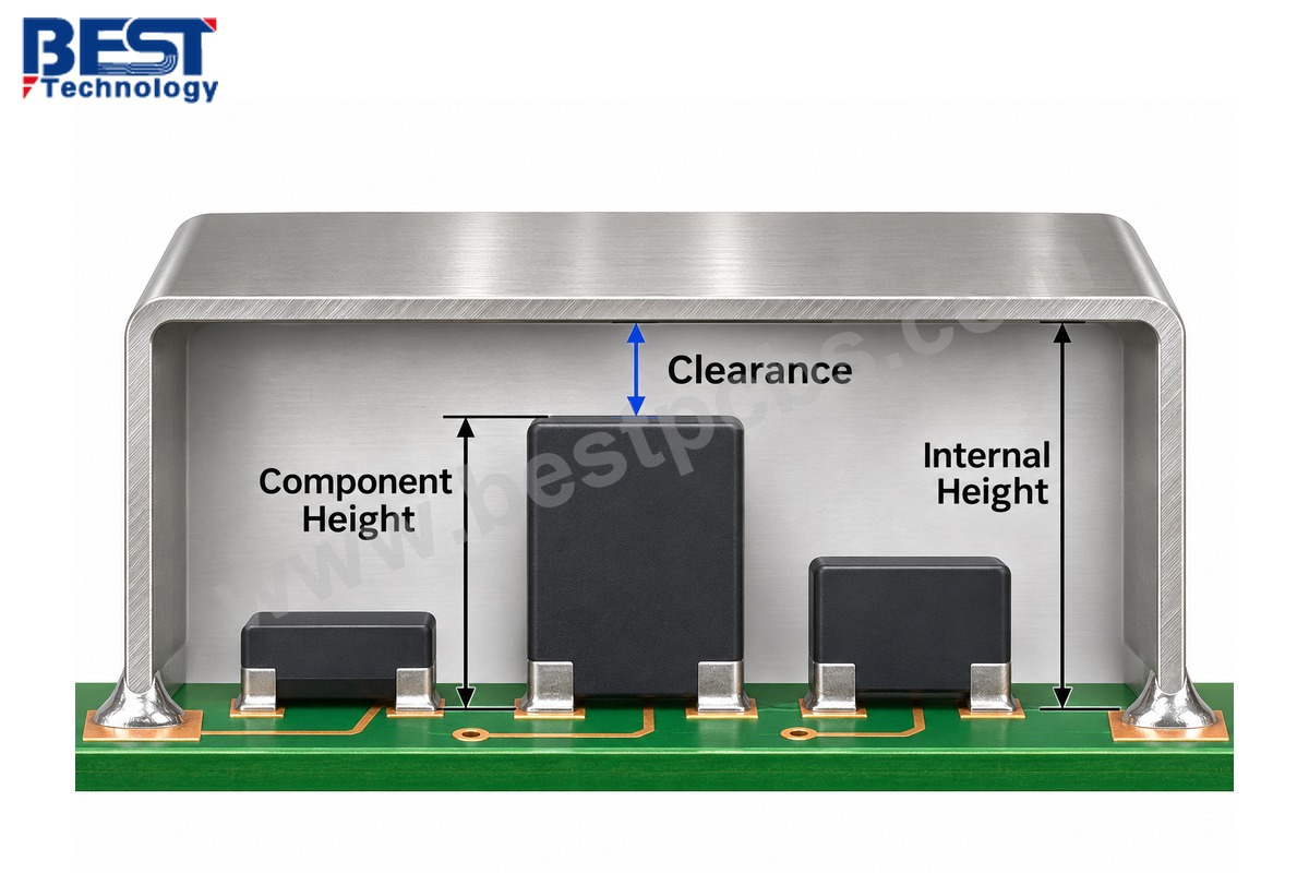
The shield’s internal space must accommodate the tallest component, its installed height tolerance, and the intended clearance beneath the cover. The footprint must also leave room for the shield walls, solder pads or clips, and neighboring parts.
The most useful dimensions are:
- Internal length and width: These define the space available for the protected circuit, including components near the walls.
- Internal height: This determines clearance above components; external cover height may include metal thickness and mounting features.
- Installed height: The assembled position of the frame or clips affects where the cover sits relative to the PCB surface.
- Wall and lid thickness: These affect available space, stiffness, and compatibility with retention clips.
- Footprint and keepout: Solder pads, tabs, clips, and tool access need space outside the protected component area.
For a simple height check, all dimensions must use the same PCB surface reference:
Minimum internal height = Maximum assembled component height + Required clearance
For example, a component with a nominal assembled height of 2.5 mm and a positive height tolerance of 0.2 mm reaches 2.7 mm. If the design allocates 0.3 mm above it, the shield needs a minimum internal height of:
2.5 + 0.2 + 0.3 = 3.0 mm
This is a dimensional example, not a universal clearance rule. The selected cover’s height tolerance, board deflection, and any required electrical spacing must fit within the design. A nominal 3.0 mm internal height is insufficient if its negative tolerance reduces the actual clearance below the requirement.
How Should an RF Shield Connect to PCB Ground?
An RF shield should connect to the PCB ground structure through short, distributed conductive connections around its perimeter. This provides a return path for shield currents and helps the cover work with the ground plane beneath the circuit.
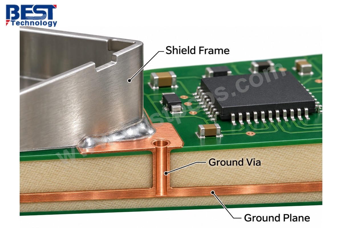
For a soldered frame, grounded pads connect the frame to the board. Nearby ground vias join those pads to the relevant plane. With a clip-mounted cover, the electrical path runs through the can, the clips, their solder joints, and the PCB ground connections.
Connection inductance becomes increasingly important as frequency rises. The inductive reactance is:
Xₗ = 2πfL
Here, Xₗ is reactance in ohms, f is frequency in hertz, and L is inductance in henries. An idealized 1 nH connection has approximately 6.3 Ω of reactance at 1 GHz, illustrating why a connection that conducts well at DC may still be unsuitable at RF.
Short connections distributed along the frame are therefore more useful than relying on a long, narrow route to a distant ground point. Plane gaps beneath the shield and poorly connected edges can also interrupt the intended enclosure.
The required via spacing depends on the frequencies and geometry involved. Our board-level shielding guide covers the related layout, opening, and grounding considerations in more detail.
When Should You Choose a Custom PCB RF Shield?
Custom PCB RF shields are useful when standard products cannot fit the available space or provide the required compartment layout. If an existing can fits the board and supports the intended assembly method, it can avoid unnecessary development and tooling work.
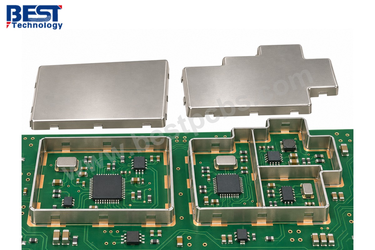
Common reasons for customization include:
- Restricted enclosure height: The product needs a cover height that standard parts do not provide.
- Irregular board layout: Connectors, mounting holes, or board edges prevent the use of a standard rectangular footprint.
- Separate circuit compartments: Internal walls must follow the positions of specific RF or analog sections.
- Dedicated access openings: An adjustment point or connector requires an opening in a defined location.
- Production-specific attachment: The design needs tabs, a pickup area, or retention features suited to its assembly process.
Custom fabrication methods also suit different quantities. Etching and forming can support development parts without a dedicated stamping die, while stamping can become attractive when repeat volume justifies tooling. Deep-drawn designs require another set of forming and tooling considerations.
What Affects PCB RF Shield Cost?
PCB RF shield cost depends on the cover’s construction, material, finish, quantity, and installation method. A catalog price usually covers the metal part alone; mounting clips, a separate lid, and assembly labor may add to the installed cost.
The main cost drivers are:
- Standard versus custom geometry: Catalog parts avoid dedicated tooling, while custom designs add development or setup costs.
- Part size and complexity: Taller walls, internal partitions, detailed retention features, and extra forming operations increase manufacturing work.
- Material and finish: Alloy choice, thickness, and plating affect both raw material and processing costs.
- Order quantity: Tooling and setup costs spread across more parts as volume increases.
- Mounting method: Placement, soldering, clip installation, and lid fitting create different assembly operations.
- Service access: A removable lid may cost more initially but reduce the work required to reach components later.
Tooling has the clearest effect at low quantities. In an illustrative calculation, $1,000 of tooling adds $10 per shield to an order of 100, but $0.10 per shield across 10,000, before material, fabrication, and assembly costs. These figures show cost allocation, not a quoted tooling price.
For a prototype, a suitable standard shield can therefore be economical even if its individual part price is higher than a future custom production part. For repeat production, the comparison shifts toward the complete installed cost and the number of operations required.
Why Choose EBest Circuit for PCB Assembly with RF Shields?
EBest Circuit manufactures RF circuit boards and provides component sourcing and PCB assembly, so customers can combine high-frequency board fabrication with shield installation in the same project. Our material options include Rogers, Taconic, and Shengyi RF laminates, alongside FR-4 for suitable control and support circuitry.
Our Rogers PCB capabilities include RO4003C, RO4350B, RO3003, and RT/duroid 5880, with additional RF material options such as Taconic RF-35 and Shengyi S7136H.
Our manufacturing and assembly capabilities include:
- Multilayer board fabrication: Our FR-4 process covers 1–10 layers as standard and 10–32 layers through special processing; RF laminate constructions receive a material-specific stackup review.
- Fine-line circuitry: For the listed 1 oz FR-4 inner and outer copper constructions, our capability is 4/4 mil line width/spacing as standard and 3/3 mil through special processing.
- Mechanical drilling: Our general PCB capability includes a 0.20 mm minimum finished hole diameter as standard and 0.15 mm through special processing, with the selected laminate and board thickness checked for the RF build.
- Shielded PCB assembly: We support SMT, through-hole, and mixed assembly, with the shield part number and footprint defining whether the build uses a soldered can, frame and lid, or retention clips.
- Sourcing and inspection: Full turnkey, partial turnkey, and consigned assembly options are available, together with solder paste inspection, AOI, and X-ray inspection where appropriate to the assembly.
For RF shield PCB assembly, we can evaluate the specified RF laminate, board construction, and shield mounting requirements together before quotation. This helps align the bare-board design with the components and mechanical parts used in the finished assembly.
FAQs About RF Shield PCBs
Is an RF shield PCB the same as an RF PCB?
No. An RF PCB carries radio-frequency circuitry and may need controlled impedance or a suitable low-loss laminate. An RF shield is a conductive enclosure added to control interference. An RF PCB may use shielding, but adding a metal can does not make an ordinary board a high-frequency laminate design.
Can an RF shield interfere with a PCB antenna?
Yes. Metal near an antenna can alter its tuning and radiation pattern, especially within the antenna’s specified keepout area. The shield normally covers the associated circuitry while leaving the radiating antenna area clear according to the antenna or module design requirements.
Can a shield can cause components to overheat?
Yes, a cover can restrict local airflow and change heat transfer around components. The PCB, thermal vias, enclosure, and any designed thermal interface must still carry heat away. Ventilation openings may help some designs, but their size and position also affect shielding performance.
Can an RF shield be added to an existing PCB?
Sometimes, if the board has suitable space and accessible ground connections. A layout with reserved shield pads or clip positions is easier to adapt. If mounting would require placing metal over exposed conductors or relying on a long ground wire, a board revision may be the better solution.
Does a PCB shield guarantee EMC compliance?
No. A shield addresses only part of the product’s interference behavior. Noise can still travel through cables, power connections, enclosure openings, and unshielded circuit areas. Compliance depends on the finished product and its applicable tests, rather than the presence of a metal cover alone.
Conclusion
The right PCB RF shield fits the circuit’s interference problem, leaves the required component access, and connects effectively to ground. Structure, material, mounting method, and available space should guide the choice before custom tooling or extra features add cost.
For PCB fabrication and assembly with RF shields, contact sales@bestpcbs.com with your PCB files, BOM, quantity, and shield part number or drawing. EBest Circuit can review the build and provide a quotation for the required manufacturing and assembly scope.