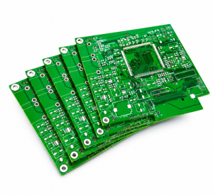
Burn-in Board is a special test board used to evaluate ICs, semiconductor devices, and electronic components under controlled temperature, voltage, current, and time stress. It is important because burn-in testing helps expose early failures before components move into real products. For semiconductor, automotive, industrial, medical, and high-reliability electronics, a burn-in board is not just a carrier board. It must support stable electrical connection, long test duration, high-temperature exposure, and reliable test repeatability.
EBest Circuit (Best Technology) supports burn-in board PCB fabrication, PCBA assembly, DFM review, PCB layout manufacturability feedback, component sourcing, testing support, and production documentation based on customer-provided files. If you are evaluating a burn-in board supplier, you can send your files to sales@bestpcbs.com. Our doors are open for on-site reviews—whenever your schedule permits, we’d be glad to walk you through our manufacturing, assembly, inspection, and traceability processes.
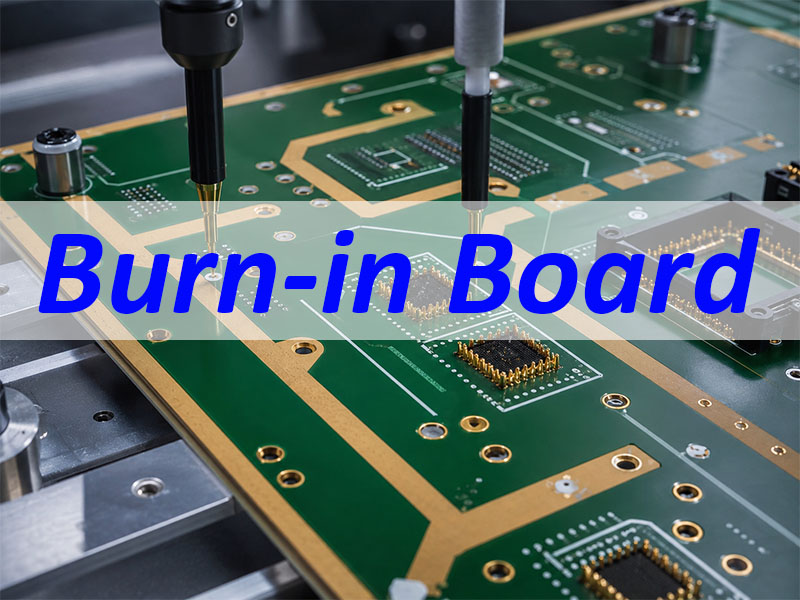
What Is a Burn-in Board?
A burn-in board is a PCB used to hold and electrically connect devices under test during burn-in testing. The device may be an IC, semiconductor package, module, or electronic component.
Key points:
- Main function: connect DUTs to a burn-in tester or test system
- Common use: IC aging test, semiconductor reliability test, high-temperature screening
- Test stress: temperature, voltage, current, signal condition, and time
- Board requirement: stable insulation, reliable copper, good flatness, and durable contact areas
- Typical industries: semiconductor, automotive electronics, industrial control, telecom, aerospace, and medical electronics
A burn-in board must remain stable during long test cycles. It may operate under high temperature and electrical stress for many hours or even several days. That is why material selection, copper spacing, hole reliability, socket area quality, and testing capability are much more important than in a normal PCB.
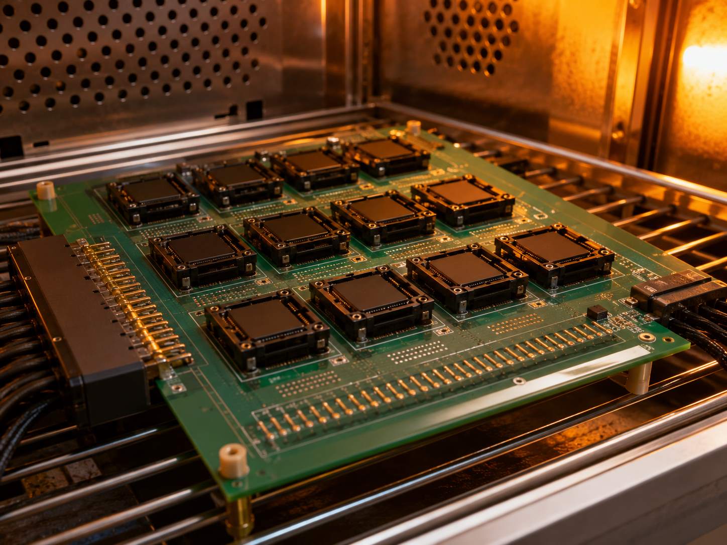
How Does a Burn-in Board Work with ICs, Sockets, and Burn-in Testers?
A burn-in board works as the interface between the device under test and the burn-in test system. It carries the DUT, routes electrical signals, and supports the mechanical connection needed during aging.
A typical burn-in board system may include:
- Burn-in board PCB
- IC sockets or contact structures
- DUT positions
- Connectors
- Test points
- Power and signal routing
- Burn-in tester connection
- Fixture or chamber interface
During testing:
- Devices are placed into sockets or test positions.
- The burn-in board connects the devices to the tester.
- The tester applies voltage, current, signals, or test patterns.
- The board may stay in a high-temperature chamber for a defined time.
- Failed or unstable devices can be identified before final use.
EBest Circuit (Best Technology) does not provide burn-in test system design or original circuit design. Our support focuses on DFM review, PCB layout manufacturability feedback, PCB fabrication, PCBA assembly, testing support, and production documentation based on the files provided by the customer.
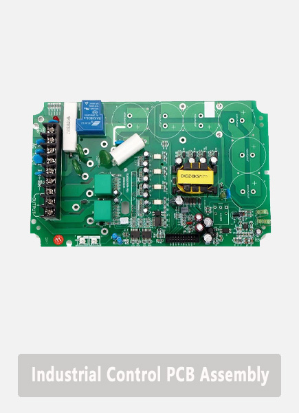
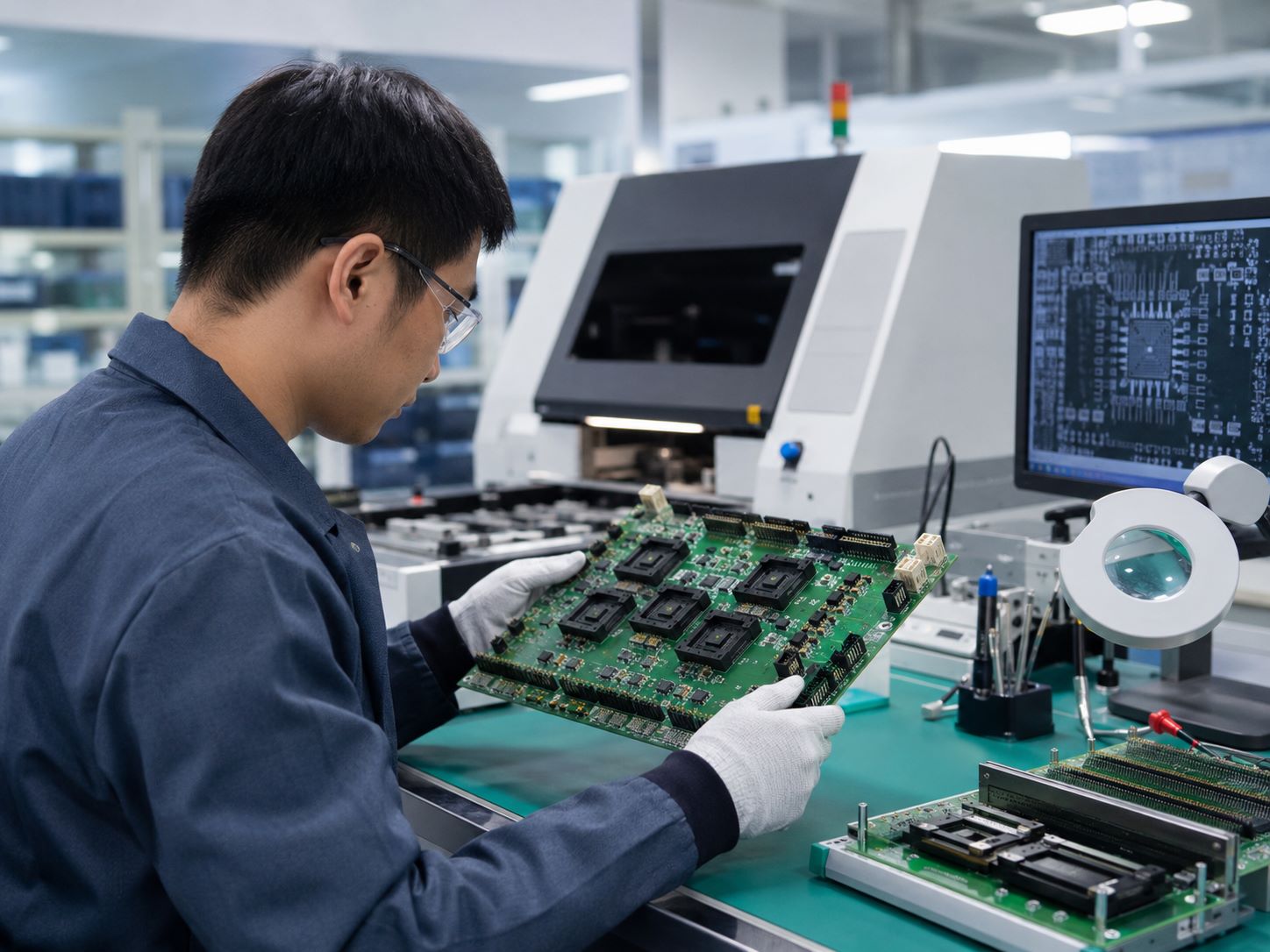
What Is a Burn-in Board PCB?
A burn-in board PCB is the printed circuit board used inside a burn-in testing setup. It may look like a test PCB, but its manufacturing requirements are often much stricter.
Compared with standard PCBs, burn-in board PCBs often need:
- Higher thermal stability
- Better insulation reliability
- Stable copper thickness
- Reliable plated through holes
- Strong socket pad durability
- Good board flatness
- High-voltage clearance control
- Long-time test reliability
- Clean surface and controlled contamination risk
Common burn-in board PCB requirements include:
- High-Tg FR4 or high-temperature material
- Multilayer structure
- Thick copper when high current is required
- ENIG or other suitable surface finish
- High-voltage spacing review
- Socket and connector area manufacturability review
- Bare-board electrical test
- Flying probe test when required
- PCBA inspection after assembly
For burn-in board PCB projects, a low price alone is not enough. A board that fails during aging may delay test validation, damage test schedules, or cost more than the board is worth.
What PCB Materials Are Used for Burn-in Boards?
Burn-in board material should be selected according to test temperature, test duration, voltage, current, device package, socket type, and reliability requirement.
Common material choices include:
- High-Tg FR4
- Suitable for many medium-to-high-temperature test boards
- Better thermal resistance than standard FR4
- Often used when cost and performance need balance
- Polyimide
- Better high-temperature performance
- Suitable for more demanding burn-in conditions
- Often considered when thermal exposure is severe
- High-temperature laminate
- Used when the board must withstand long aging cycles
- Helps improve dimensional and insulation stability
- Heavy copper material
- Used when the board carries higher current
- Supports power stress and thermal load requirements
- Special surface finishes
- ENIG is common for socket, contact, and assembly reliability
- Final choice depends on soldering, socket contact, and test conditions
Material selection should be confirmed before production. If the customer’s burn-in temperature, voltage, time, or socket requirement is unclear, EBest Circuit (Best Technology) can raise engineering questions before manufacturing.
What Manufacturing Challenges Affect Burn-in Board PCB Reliability?
Burn-in boards are built for stress. The manufacturing process must support temperature, voltage, current, and repeated testing conditions.
Key manufacturing challenges include:
- High-temperature stability
- Material must remain stable during long burn-in cycles.
- Board warpage and delamination risk must be controlled.
- High-voltage insulation
- Clearance and creepage areas must be reviewed.
- Contamination, exposed copper, and insufficient spacing may increase leakage risk.
- Hole wall reliability
- Plated through holes must remain reliable under thermal cycling.
- Poor hole copper can create open circuits or unstable resistance.
- Socket and contact areas
- Socket pads need stable surface finish and solderability.
- Pad damage or poor flatness can affect test consistency.
- Copper thickness and current
- High-current paths may need thicker copper.
- Thermal rise should be considered during manufacturability review.
- Board flatness
- Warpage may affect socket contact, fixture mounting, and PCBA assembly.
- Panelization and pressing process should be reviewed.
- Testing and inspection
- Bare-board electrical test
- Leakage test if required
- Flying probe test
- AOI
- X-ray for PCBA when required
- Final documentation
A burn-in board manufacturer should not do whatever just to lower the quoted price. The real goal is to make a board that survives the test environment and supports stable long-term evaluation.
Burn-in Board Case Study: 200°C High-Voltage Aging Test Project
This case came from a customer evaluating a long-term burn-in board supplier. The customer made the selection criteria clear from the beginning: quality, price, technical capability, service response, and lead time. If these points were acceptable, the project could become a long-term cooperation.
Project Overview
- Burn-in board project for early supplier evaluation
- High-temperature aging requirement
- High-voltage burn-in condition
- PCB and PCBA test capability required
- Long-term cooperation potential
Customer Requirements
- PCB working condition: 200°C
- Burn-in time: more than 168 hours
- Burn-in voltage: above 1200V
- Bare PCB leakage test required
- Flying probe test capability required
- PCBA capability required
- PCBA-level test and fly-scope test capability required
EBest Circuit (Best Technology)’s Review Focus
For this type of burn-in board project, the engineering review should focus on reliability, manufacturability, and test feasibility.
Key review points include:
- High-temperature material suitability
- High-voltage clearance and creepage manufacturability
- Copper spacing and exposed copper risk
- Hole wall reliability during long aging time
- Surface finish and solderability
- Bare-board leakage test requirement
- Flying probe test feasibility
- PCBA assembly process review
- Socket, connector, and test point manufacturability
- Shipment report and inspection documentation
Project Value
This case shows why burn-in board manufacturing should not be evaluated only by board price. At 200°C, 168+ hours, and 1200V+, the board needs material stability, insulation reliability, test capability, and clear engineering communication.
When customers provide demanding test conditions early, we can better appreciate what we get from the project files: not just dimensions and Gerbers, but the actual reliability environment the board must survive.
What Should You Check When Choosing a Burn-in Board Manufacturer?
Choosing a burn-in board manufacturer is different from choosing a general PCB supplier. The board may need to work under high temperature, high voltage, repeated test cycles, and strict reliability conditions.
When comparing burn-in board manufacturers, check these points:
- High-temperature PCB experience
- High-Tg FR4
- Polyimide
- High-temperature laminate
- Thermal stability review
- High-voltage manufacturability
- Clearance review
- Creepage review
- Leakage risk awareness
- Copper-to-copper spacing review
- PCB fabrication capability
- Multi-layer PCB
- Thick copper PCB
- Controlled board thickness
- Reliable plated through holes
- ENIG and other surface finishes
- Testing support
- Bare-board electrical test
- Flying probe test
- Leakage test when required
- AOI
- X-ray for PCBA when needed
- PCBA assembly support
- Socket assembly
- Connector assembly
- SMT and DIP support
- Test point and fixture-related review
- Engineering communication
- DFM review
- PCB layout manufacturability feedback
- Engineering questions before production
- Production documentation support
Burn-in boards should not be sent to all and sundry as if they were ordinary FR4 boards. A suitable supplier should understand the test environment and review the manufacturing risks before production starts.
EBest Circuit (Best Technology) is an engineer-oriented one-stop PCB service provider. We support PCB fabrication, PCBA assembly, testing, and documentation for suitable burn-in board projects based on customer-provided files.
What Files Are Needed for a Burn-in Board PCB Quote?
Customers do not need perfect documentation before contacting EBest Circuit (Best Technology). Available files can be sent first, and missing details can be clarified during engineering review.
For initial quotation, these files are helpful:
- Gerber files
- Drill files
- Board size
- Layer count
- Material requirement
- Board thickness
- Copper thickness
- Quantity
- PCB only or PCBA requirement
For a more accurate burn-in board quote, please add if available:
- Stack-up
- Surface finish
- Burn-in temperature
- Burn-in voltage
- Burn-in time
- Current requirement
- Clearance or creepage requirement
- Socket or connector specification
- Test requirement
- Leakage test requirement
- Report requirement
For PCBA quotation, please add:
- BOM
- Pick and place file
- Assembly drawing
- Socket or connector datasheet
- Functional test notes, if any
- Special handling or packaging notes
Cost is usually affected by:
- Material type
- Layer count
- Board size
- Copper thickness
- High-voltage spacing
- Socket quantity
- Assembly complexity
- Testing requirement
- Report requirement
- Order quantity
For review, send your available burn-in board files and test requirements to sales@bestpcbs.com. We can also arrange a factory visit at a convenient time if you would like to evaluate our PCB fabrication, PCBA assembly, inspection, and traceability process in person.
FAQs About Burn-in Board
What is a burn-in board?
A burn-in board is a PCB used to connect ICs, semiconductor devices, or electronic components to a burn-in tester during aging or reliability testing.
What are burn-in boards used for?
Burn-in boards are used to test devices under stress conditions such as high temperature, voltage, current, and long operating time. They help identify early failures before final use.
What is a burn-in board PCB?
A burn-in board PCB is the physical printed circuit board used in burn-in testing. It must support stable electrical connection, high-temperature operation, and long test duration.
What is an IC burn-in board?
An IC burn-in board is a burn-in board used specifically for integrated circuits. It usually includes IC sockets, test positions, connectors, and routing for the burn-in tester.
What is the difference between a burn-in board and a test board?
A test board may be used for many types of electrical checks. A burn-in board is used for aging under stress conditions, often involving high temperature and long test time.
What PCB materials are used for burn-in boards?
Common options include High-Tg FR4, polyimide, high-temperature laminates, and heavy copper structures when higher current is required. The material depends on temperature, voltage, time, and test conditions.
How much does a burn-in board cost?
Burn-in board cost depends on material, layer count, board size, copper thickness, socket quantity, assembly complexity, testing, documentation, and quantity. A cheaper option may cost more than the board is worth if it fails during reliability testing.
What files are needed for a burn-in board PCB quote?
Gerber files, drill files, material requirement, board thickness, copper thickness, quantity, test temperature, test voltage, and PCBA requirements are helpful. BOM, pick and place file, assembly drawing, and socket information are needed for PCBA quote.
Can EBest Circuit (Best Technology) support burn-in board PCB fabrication and assembly?
Yes. EBest Circuit (Best Technology) supports burn-in board PCB fabrication, PCBA assembly, DFM review, PCB layout manufacturability feedback, testing support, and production documentation based on customer-provided files.
How can I start a burn-in board quotation?
Send your available files, test conditions, and assembly requirements to sales@bestpcbs.com. EBest Circuit (Best Technology) will review the project and advise what extra information is needed before production.