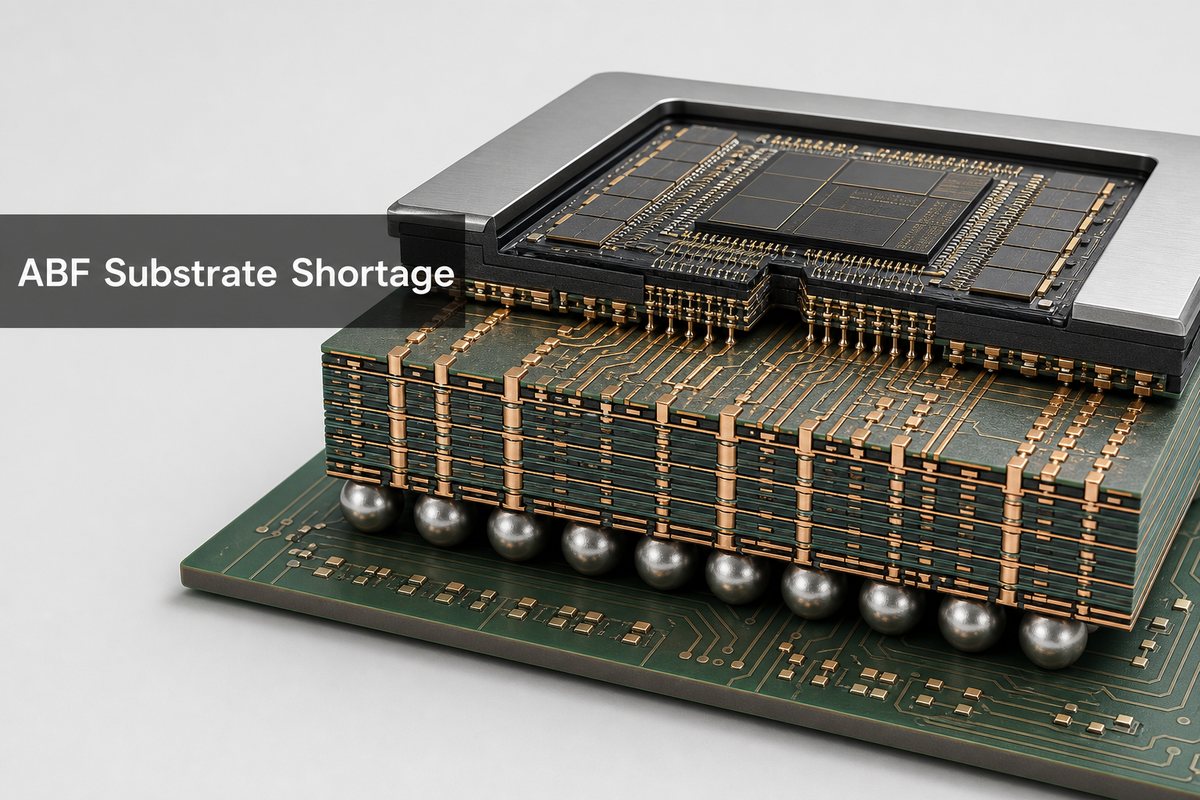
The ABF substrate shortage is becoming a high-end AI packaging constraint rather than a broad shortage affecting every substrate equally. Counterpoint Research estimated an ABF supply gap of about 10% in the second half of 2026, widening to 20% in 2027 before new capacity comes online.
The risk is concentrated in large, multilayer package substrates that consume more low-CTE glass cloth, ABF dielectric, semi-additive-process capacity, and inspection time. Buyers should qualify the exact package construction and supplier allocation instead of treating the forecast as a universal lead-time or price increase.
What Is Causing the ABF Substrate Shortage?
The shortage is being driven by rapid AI-package growth, larger substrate area, higher layer counts, constrained low-CTE T-glass, and the slow ramp of qualified high-end capacity. These pressures reduce the number of advanced packages that an existing line can produce even when the nominal panel count looks unchanged.
Counterpoint Research described a structural up-cycle tied to enterprise AI demand and estimated that one AI chip can consume roughly ten times the substrate material of a standard PC chip. That is an industry estimate, not a design rule for every package, but it explains why mix shift matters as much as unit demand.
What Is ABF Substrate Material and Film?
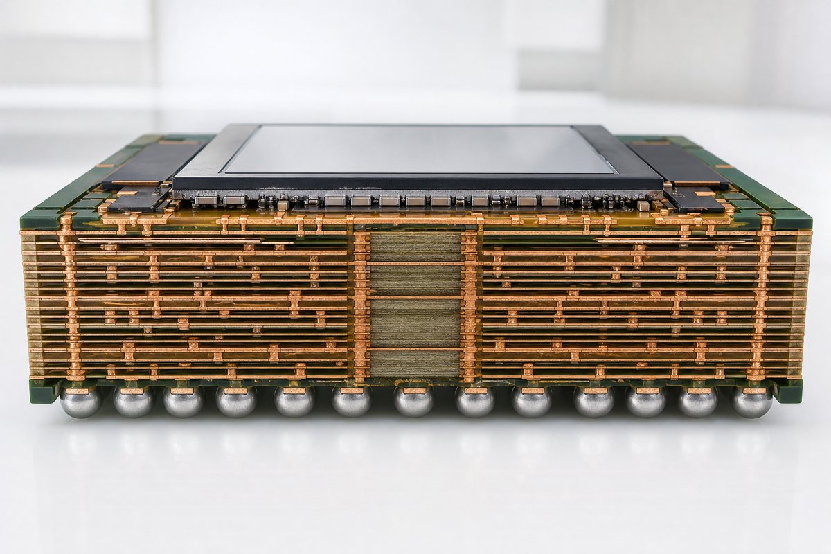
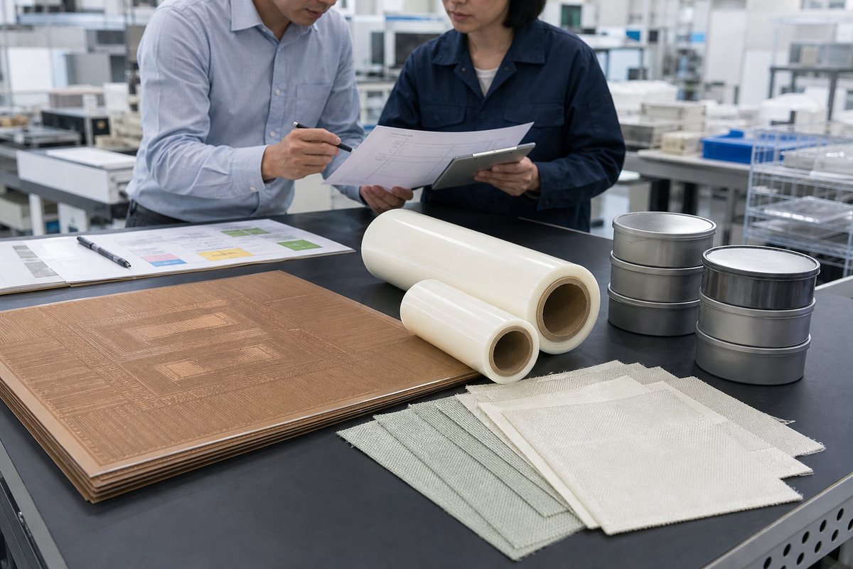
ABF substrate material is an organic build-up system used to route very fine connections between a high-performance semiconductor die and the larger-pitch PCB below it. ABF substrate film is the interlayer dielectric used between copper routing layers; laser processing and direct copper plating help form the dense interconnect structure.
Ajinomoto explains that ABF combines organic epoxy chemistry with inorganic microparticle filler to provide insulation, low thermal expansion, durability, and processing characteristics for advanced package substrates. The film is one part of a complete substrate that also includes copper circuitry, a core or coreless structure, vias, solder mask, surface finish, and BGA connections.
How Large Is the 2026–2027 Supply Gap?
The current public forecast points to a roughly 10% ABF gap in the second half of 2026 and a 20% gap in 2027. These figures should be treated as analyst estimates for the industry, not guaranteed shortages for every supplier, package type, or customer contract.
| Period | Public Signal | Buyer Interpretation |
| H1 2026 | 3–5% quarter-over-quarter substrate price increases expected | Quotes may be revised as material and capacity costs move |
| H2 2026 | About 10% ABF supply gap forecast | High-end allocation and schedule risk become more visible |
| 2027 | Gap forecast to widen to about 20% | New capacity starts, but demand and qualification may outpace ramp |
| From FY2027 | IBIDEN plans sequential new mass-production capacity | Capacity relief depends on equipment, qualification, yield and customer mix |
Why Does Low-CTE T-Glass Matter?
Low-CTE T-glass helps control dimensional stability and warpage in large, thin, multilayer organic packages. As package size and layer count increase, the substrate must survive lamination, thermal cycles, assembly, and operation while keeping fine features aligned.
Counterpoint estimated a T-glass supply-demand gap above 10% in 2026. A shortage of qualified glass cloth can restrict both ABF substrate output and high-end copper-clad laminate, even if a substrate manufacturer has available imaging, plating, and drilling equipment. An alternate glass style is not automatically interchangeable; resin compatibility, thickness, CTE, electrical properties, process behavior, and package reliability must be validated.
How Do Larger AI Packages Consume More Capacity?
Larger AI packages consume capacity through area, layer count, process steps, inspection burden, and yield—not just unit volume. More build-up layers require repeated lamination, laser-via formation, desmear, metallization, imaging, plating, etching, and inspection cycles.
- More substrate area: fewer units may fit on a panel, and each defect affects more value.
- More routing layers: repeated build-up cycles occupy equipment for longer.
- Finer features: tighter process windows raise inspection and yield demands.
- Warpage control: larger packages need more precise material and process matching.
- Embedded or advanced structures: additional failure points can reduce effective output.
IBIDEN’s 2026 results presentation indexed the production load for an AI-server substrate at 1.8 times its 2024 level in 2026 and 2.5 times in 2028 when converted by semi-additive-process demand.
Which Price and Lead-Time Signals Matter?
The most useful signals are configuration-specific quotes, allocation confirmation, material status, committed capacity, qualification status, and delivery milestones. Broad market percentages do not replace a supplier’s documented production plan.
| Signal | What to Request | Decision Use |
| Material allocation | ABF film, glass cloth, core and copper availability by construction | Tests whether the quoted stack is actually supported |
| Qualified capacity | Committed line, approved process and customer qualification status | Separates installed equipment from usable output |
| Price validity | Validity period and material-adjustment mechanism | Defines exposure between quote and release |
| Milestones | Material receipt, start, inspection, shipment and recovery dates | Provides an auditable schedule |
| Yield assumptions | Sampling, inspection and disposition rules | Shows how defects could affect delivery |
How Are ABF Substrate Manufacturers Expanding Capacity?
ABF substrate manufacturers are investing heavily, but high-end capacity takes time to install, qualify, and stabilize. IBIDEN announced an approximately JPY 500 billion investment plan for FY2026–FY2028, focused on high-performance IC package substrates for AI and high-performance servers, with sequential operation and planned mass production beginning in FY2027.
IBIDEN also stated that larger and more multilayered substrates are expected to push total semi-additive-process demand beyond industry supply capacity. Buyers should therefore distinguish a capital-spending announcement from qualified volume that is available to their exact package and schedule.
What Should Buyers Ask ABF Substrate Suppliers?
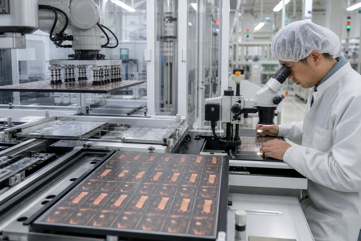
ABF substrate suppliers should answer against the exact package construction, not only a generic product family. A useful sourcing review covers materials, manufacturing site, qualified process, capacity commitment, inspection, change control, and recovery planning.
- Which ABF film grade, glass style, core construction, and copper system are quoted?
- Are all materials allocated for the requested prototype and production quantities?
- Which site and production line are qualified for this package?
- What changes require customer notification and requalification?
- How are warpage, layer registration, microvias, copper thickness, continuity, and surface defects inspected?
- What is the recovery plan if material or yield misses the committed milestone?
For terminology and structure differences, see our IC substrate overview and guide to IC substrate types and materials.
How Does the Shortage Affect PCBA Planning?
The substrate shortage can delay packaged processors before those components ever reach the PCBA line. A PCB assembler may have bare boards, passive components, and production capacity ready while waiting for the processor or accelerator package.
Project plans should link package delivery milestones to PCB fabrication, component kitting, stencil release, assembly slots, firmware readiness, and test-fixture availability. Avoid building a schedule that assumes every upstream item will arrive on the same day. The distinction between a BT substrate and a high-end ABF substrate also matters because material allocation and package applications differ.
Which Design and Qualification Actions Reduce Risk?
Risk falls when the team freezes the package interface early, keeps alternates evidence-based, and plans qualification before a shortage forces a change. Late substitutions are especially dangerous when they alter substrate dimensions, ball map, electrical behavior, warpage, thermal path, or assembly profile.
- Freeze the package outline, ball map, PCB land pattern, keep-outs, and thermal interface.
- Record the approved substrate construction and material set.
- Qualify alternates before allocation becomes critical.
- Align substrate, component, PCB, assembly, and test milestones in one schedule.
- Define incoming inspection, traceability, change notification, and nonconformance handling.
FAQ About ABF Substrate Shortage
- Is every ABF substrate in shortage?
-
No. The pressure is strongest in high-end, large, multilayer substrates for AI and advanced computing. Supplier allocation, construction, customer qualification, and contract status determine the actual risk.
- What is the difference between ABF film and an ABF substrate?
-
ABF film is the insulating build-up dielectric. The finished substrate combines that dielectric with copper circuitry, vias, a core or coreless structure, solder mask, surface finish, and package connections.
- Why does new factory capacity not solve the shortage immediately?
-
Equipment installation is only one step. Materials, process qualification, customer approval, yield ramp, inspection capacity, and product mix determine when usable output becomes available.
- Will substrate prices rise by the same percentage for every buyer?
-
No. Public percentages are market estimates. The actual change depends on package size, layers, materials, committed capacity, order volume, contract terms, timing, and supplier relationship.
- Can a PCB fabricator replace an ABF package substrate?
-
Not directly. An advanced IC package substrate uses different feature sizes, processes, materials, equipment, quality controls, and semiconductor-package qualifications from a conventional PCB.
How Can EBest Circuit Support Substrate and PCB Planning?
EBest Circuit supports PCB design, PCB fabrication, component sourcing, PCB assembly, prototyping, mass production, and engineering review. For projects exposed to package-substrate constraints, send us the Gerber files, BOM, stack-up, package details, quantities, approved alternates, testing requirements, and target schedule. We can review the downstream PCB and PCBA plan and provide a project-specific quotation at sales@bestpcbs.com.