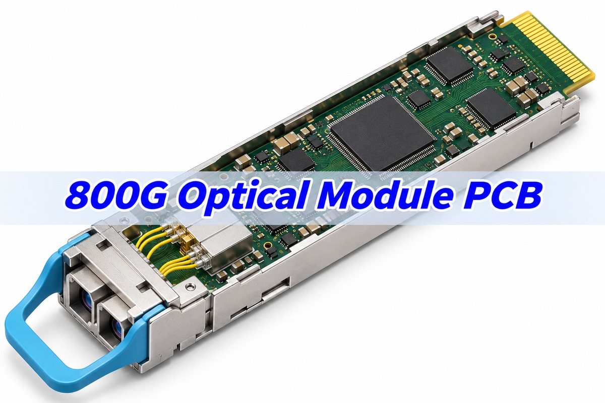
An 800G optical module PCB is the circuit board inside a pluggable transceiver. It carries the host’s electrical signals from the module’s edge contacts to devices that process those signals and interface with the optics. It also distributes power and connects the module’s control circuitry. The PCB does not carry light along its copper traces; that job belongs to the optical path.
In a QSFP-DD800 design, the host interface uses eight electrical lanes in the 100 Gb/s class. The design question is how much loss those lanes can tolerate between the specified reference points, not which laminate has the lowest dissipation factor on paper.
Key Takeaways
- The module PCB is separate from the switch host board. Both can contribute loss, depending on where the interface specification defines its measurement planes.
- 800G is the aggregate rate. QSFP-DD800 uses eight 100 Gb/s-class host electrical lanes; that does not fix the module’s optical lane arrangement.
- Choose the stackup using routed length, reference planes, laminate loss and foil roughness together. An impedance match does not establish low insertion loss.
- Model the edge launch and via transitions. A short trace does not make a poor transition harmless.
- Check loss on a representative coupon, then validate the actual electrical path and thermal performance in the assembled module.
What Does an 800G Optical Module PCB Connect?
The PCB connects the host edge fingers to the module electronics and provides the electrical connections to the optical subassemblies. In a DSP-based design, the host lanes typically route to a digital signal processor. The transmit path then drives the optical transmitter; on receive, a photodetector and transimpedance amplifier convert the received light into an electrical signal for downstream processing.
An 800G optical module teardown can help identify where these parts sit. It cannot tell you the inner-layer geometry or foil grade. Those details come from the design files and the fabricator’s stackup.
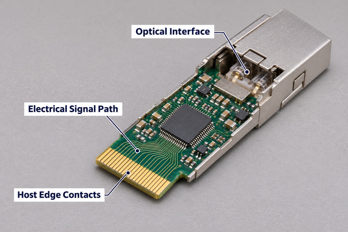
At EBest Circuit, we review controlled-impedance PCB requirements against the proposed stackup. For a module board, that means checking whether the requested dielectric thicknesses, pair dimensions and drill structure can fit the outline and be fabricated together. This is board-level support, separate from optical module qualification.
What Does 800G Mean for the Electrical Lanes?
For QSFP-DD800, 800 Gb/s is the aggregate rate over eight 100 Gb/s-class electrical lanes. The QSFP-DD MSA hardware specification also describes electrical operation up to 112 Gb/s per lane at 56 GBd with PAM4. Use the rate and frequency requirements of the specific interface, not the aggregate number, when setting up the channel model.
Separate the host interface from the optical designation. For example, 800G QSFP-DD products can differ in their fiber connectors and optical configurations, even though they use the same module family. Likewise, an 800G OSFP module is not mechanically interchangeable with a QSFP-DD module just because their aggregate rates match.
How Do You Set an 800G Optical Module PCB Loss Budget?
Start with the specified electrical reference planes and allocate part of the permitted loss to the PCB route and its transitions. Draw the path between those planes before adding numbers. The host connector, edge-finger launch, vias and package transition only belong in the calculation where the interface definition includes them.
| Channel feature | What to model or measure |
|---|---|
| Uniform differential pair | Insertion loss versus frequency for the actual layer, width, spacing and route length |
| Edge-finger launch | Return loss and insertion loss using the actual contact and board-edge geometry |
| Layer transition | Via barrel, residual stub, antipad and nearby ground-return vias |
| Adjacent lanes | Coupling where pairs run close together, especially near dense pin fields |
For an illustrative calculation, a 0.8-inch route with modeled loss of 1.5 dB/in at 28 GHz contributes about 1.2 dB at that frequency before launches and vias. Neither number is an 800G requirement. Use the actual model and simulate the cascaded path when reflections matter rather than treating a simple sum as a compliance result.
How Do You Choose an 800G Optical Module PCB Stackup?
For an 800G optical module PCB, choose signal layers with continuous reference planes and enough room to hold differential impedance along the route. A short outer-layer route may avoid a via transition. An inner stripline route can give the pair a more controlled environment, but it adds transitions at both ends if the endpoints are on the surface.
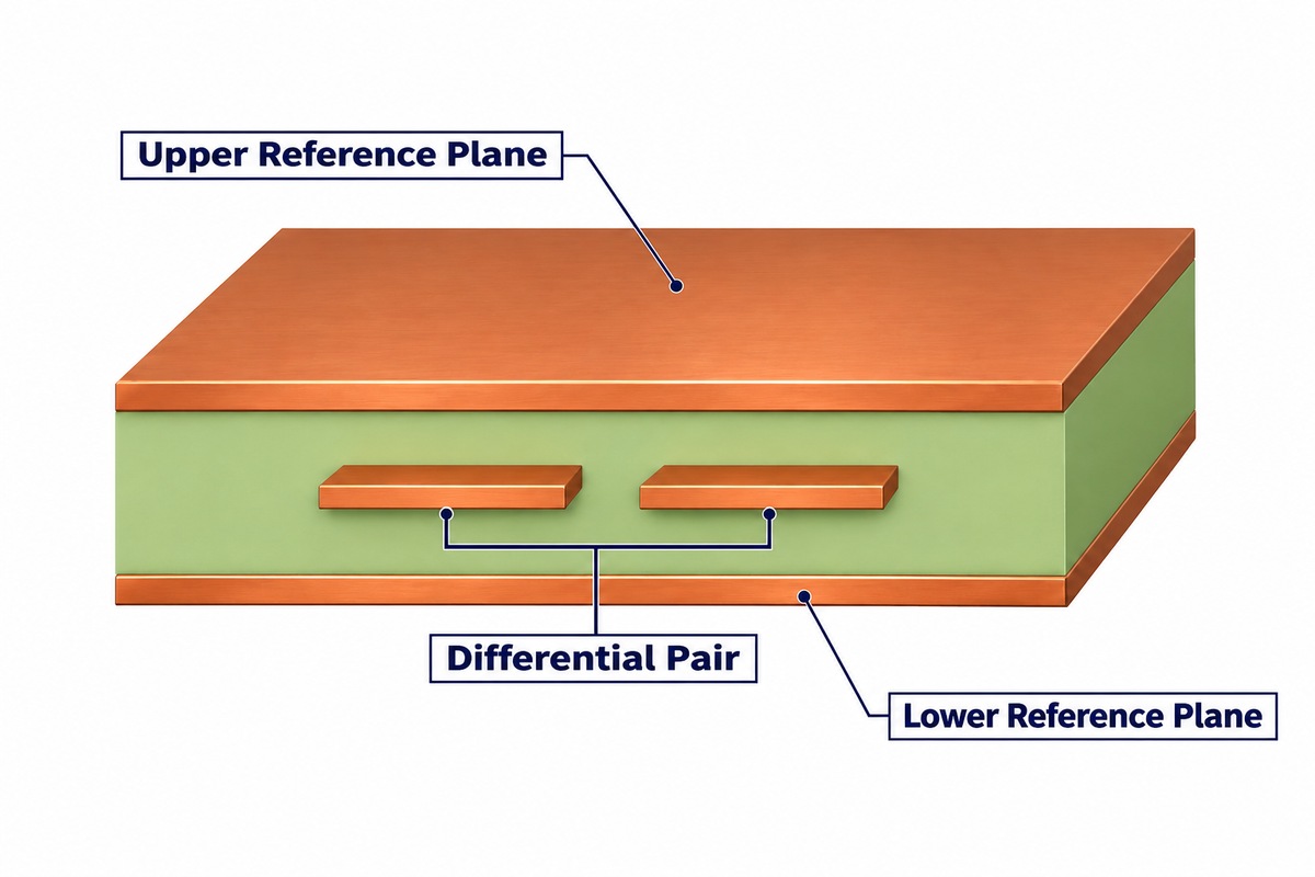
Set the electrical stackup alongside the module mechanics. Finished board thickness and the edge interface constrain the available build. Ask the fabricator to return a proposed construction with the actual core and prepreg thicknesses, copper thickness and achievable trace dimensions before locking the artwork.
Which Laminate and Copper Foil Should You Specify?
Specify a laminate and foil combination that meets the board’s insertion-loss allocation using the proposed geometry. The dielectric’s dissipation factor, or Df, contributes to dielectric loss. Copper roughness contributes to conductor loss. A low-Df material can still miss the budget if the foil profile or routing geometry raises conductor loss.
Compare candidate materials using compatible test frequencies and methods. On the drawing or stackup, name the laminate grade and foil profile rather than writing only “low loss.” Make any alternative material subject to a review of the stackup and electrical model. Our guide to high-speed PCB materials explains how Dk, Df and foil profile fit into that comparison.
Which Via Transitions Need Review on an 800G Optical Module PCB?
Give a transition extra attention when the model shows a return-loss problem, a dip in insertion loss, or unacceptable coupling to nearby lanes. In a plated through-via, the unused barrel below or above the target layer can act as a stub. Shortening it may help, but a via with little or no stub can still reflect if the pad, antipad or return geometry is poor.
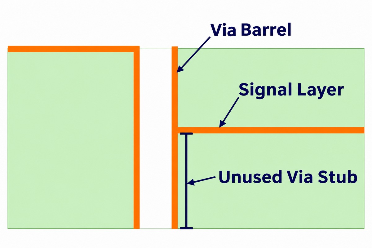
On an existing 800G optical module PCB, compare layer reassignment, a manufacturable backdrill or a blind-via transition using the same electrical reference planes. Review the actual residual-stub tolerance rather than simulating an ideal zero-stub via. Include the edge contact, reference-plane openings and ground connections when modelling the launch.
How Does Module Power Consumption Affect the PCB?
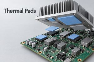
800G transceiver power consumption affects the board’s power delivery and the heat path from its components to the enclosure. For example, Cisco lists maximum power consumption of 15 W for its QDD-800G-VR8 and 17 W for its QDD-8X100G-FR. These are whole-module ratings for those models, not per-chip heat loads or a universal 800G limit. Use the module’s own power limits and evaluate where the heat is generated, how it reaches the case and how the cage and airflow remove it.
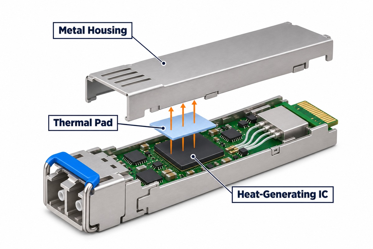
In a compact assembly, moving the DSP to improve thermal contact can lengthen an electrical route. Check its location with the mechanical model before releasing either design. Include component height, thermal interface contact and the intended case-temperature measurement point in the review.
What Should You Verify on the First Build?
Verify the fabricated electrical geometry first, then test the assembled path at the specified measurement points. A controlled-impedance coupon can confirm impedance for the represented construction. It does not prove the module launch or the complete signal path meets its loss limits.
- Check the actual stackup, foil and drilling against the approved construction.
- Measure impedance and, where required, frequency-dependent insertion loss on representative structures. Document calibration and the fixture removal method.
- Measure the relevant assembled electrical path, including its transitions. Use an appropriate interface test to check link performance under the required conditions.
- Run the module in its representative cage and airflow. Verify temperature limits and link operation together at the required operating points.
FAQ About 800G Optical Module PCBs
Is every 800G module board an HDI PCB?
No. The need for HDI comes from the package escape, routing density, board thickness and transition geometry. The 800G label does not prescribe a via technology or layer count.
Can a passing impedance coupon replace insertion-loss testing?
No. The coupon may verify impedance, but dielectric and conductor losses can still be too high. Specify a suitable loss coupon or assembled-path measurement if loss is an acceptance criterion.
Is 28 GHz a universal acceptance frequency?
No. It is the Nyquist frequency in a 56 GBd example. Use the frequencies, masks and reference planes specified for the interface you are validating.
Can the PCB fabricator certify the finished optical link?
Bare-board results do not certify the optical link. Validate the complete module against the specified electrical, optical and thermal requirements after assembly.
Can two nominally equivalent laminates share the same artwork?
Only after checking the actual construction. Different dielectric thicknesses, design Dk or foil profiles can shift impedance or loss even when the process uses the same nominal material family.
What Should You Share for a Module PCB Review?
Send the outline, proposed stackup, electrical interface, target impedance, loss allocation and critical via or edge-contact details to sales@bestpcbs.com. If the enclosure fixes the board thickness or component height, include those limits too. We can review them alongside your fabrication and PCB assembly requirements.