2N2222 pinout looks like a small three-pin detail, but it can decide whether a transistor footprint, BOM substitute, and assembled PCBA work correctly after production. For PCB buyers and engineers, the main risk is not knowing that the same transistor name may appear in different packages, views, or supplier drawings.
Before PCB fabrication or PCBA assembly, the emitter, base, and collector must match the exact datasheet, package outline, PCB footprint, silkscreen mark, and assembly direction. A wrong pin order can pass a quick visual check but fail during functional testing, rework, or field use.
EBest Circuit (Best Technology) supports PCB fabrication, PCB layout manufacturability review, component sourcing coordination, PCBA assembly, inspection, and testing support for transistor-based control boards. If you need help checking a 2N2222 transistor footprint or assembly file before production, contact sales@bestpcbs.com.
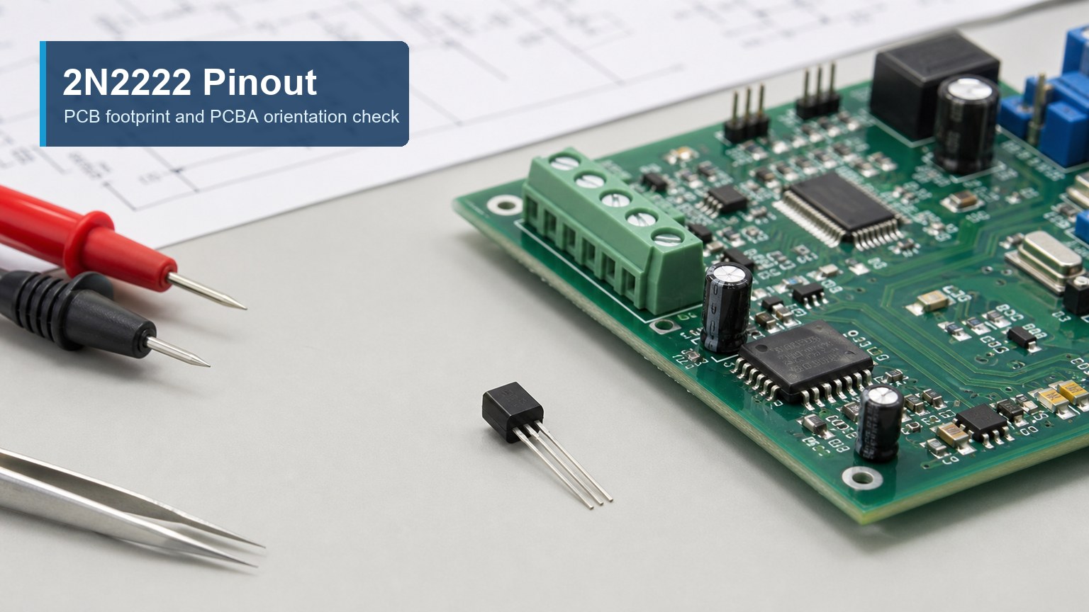
What Is the 2N2222 Pinout?
The 2N2222 pinout is the pin assignment for the three terminals of a 2N2222 NPN bipolar junction transistor. The terminals are emitter, base, and collector.
The simple explanation is:
- Emitter: current exits the transistor in typical NPN switching circuits.
- Base: receives the control signal through a suitable resistor.
- Collector: connects to the load side in many low-power switching designs.
That sounds simple, but it is not enough for production. The pin order depends on the exact part number, package, manufacturer datasheet, and how the transistor is viewed. A TO-92 part shown from the flat face may not match a metal-can package or an SMD package. Even similar names such as 2N2222A, PN2222A, and P2N2222A should be checked against the selected manufacturer datasheet.
For a PCB or PCBA order, the safest wording is not “2N2222 is always E-B-C.” The safer production instruction is: confirm the manufacturer part number, package, pin view, PCB footprint, and assembly orientation before release.
2N2222 Transistor Pinout and Pin Functions
A 2N2222 transistor is commonly used as a small-signal NPN transistor for switching and amplification. In many PCB products, it may drive LEDs, relays, buzzers, small motors, signal lines, or interface circuits.
Buyers usually need to confirm these pin functions before PCBA:
| Pin Function | What to Check in Production Files | Risk if Wrong |
| Emitter | Connected to the correct reference or return path. | The transistor may not switch correctly. |
| Base | Controlled through the correct resistor network. | The transistor may stay off, overheat, or behave unstably. |
| Collector | Matched to the load side and current path. | The load may fail to operate or the part may be damaged. |
For assembly teams, the pin function is only useful when it is tied to the physical footprint. A schematic may be correct, but the PCB symbol-to-footprint mapping can still be wrong. This is why transistor pinout checks should include the schematic symbol, PCB footprint pads, BOM manufacturer part number, and placement drawing.
2N2222 Pin Configuration by Package Type
The phrase “2N2222 pin configuration” often creates confusion because users may be looking at different package types. A TO-92 plastic package, TO-18 metal can, and SMD transistor package cannot be treated as one fixed layout.
Common package review points include:
- TO-92: confirm whether the drawing is viewed from the flat face or lead side.
- TO-18 metal can: confirm the bottom-view or top-view reference in the datasheet.
- SOT-23 or other SMD substitutes: confirm the exact substitute part and footprint.
- PN2222A or P2N2222A: do not assume the same pin order as another supplier’s 2N2222.
In real sourcing work, the project may start with “2N2222” in the BOM, but the available part may be a manufacturer-specific 2N2222A, PN2222A, P2N2222A, or SMD equivalent. The electrical replacement may look acceptable, but the footprint and pin order still need a separate check.
2N2222 Pin Diagram Mistakes Before PCB Layout
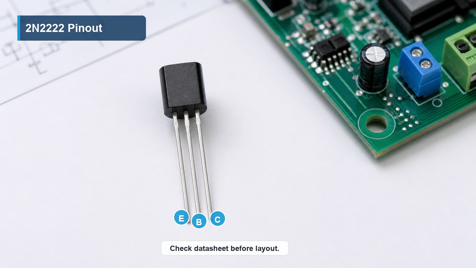
A 2N2222 pin diagram can be correct on its own but still cause a wrong PCB if the view direction is misunderstood. Many drawings show the package from a specific side, and that side is easy to reverse during footprint creation.
Common mistakes before layout include:
- Reading a bottom-view drawing as a top-view drawing.
- Copying a generic internet pinout without checking the chosen manufacturer.
- Using a TO-92 footprint for a different lead order.
- Replacing a through-hole part with an SMD part without footprint review.
- Leaving the flat-side mark unclear on the silkscreen.
- Letting the BOM name and assembly drawing describe different packages.
For a single prototype, one wrong footprint may be repaired by cutting traces or bending leads. For a batch build, the same error can stop assembly, delay shipment, and create extra component and labor cost.
A practical DFM review should ask one direct question: if an operator looks at the PCB, BOM, and placement drawing, can they install the transistor in only one correct orientation?
2N2222A Pinout and PN2222A Pinout Differences
2N2222A and PN2222A are often discussed together because both are common NPN transistor options. However, their pinout should not be judged only by the name. The package and manufacturer matter.
For BOM substitution, check these items before approval:
- Full manufacturer part number
- Package code and drawing
- Pin assignment and view direction
- Collector current and voltage rating
- Power dissipation and thermal condition
- Gain range or hFE grouping
- Lead forming or tape packaging requirement
- Footprint compatibility with the PCB
From the buyer’s side, this is where component sourcing and assembly review should work together. A purchasing team may find an available substitute, but the engineering review must confirm whether it can be assembled on the same PCB without changing the footprint or circuit behavior.
EBest Circuit can help flag these sourcing-related manufacturing risks before production. The final electrical approval should still come from the customer’s engineering team, especially when the transistor is used near its voltage, current, gain, or thermal limits.
How to Check the 2N2222 Datasheet Before PCB Footprint Selection
The datasheet is the authority for footprint selection. Search results and quick diagrams can help explain the topic, but they should not replace the selected manufacturer’s datasheet in a production build.
A datasheet check should confirm:
- Exact package outline
- Lead order and view direction
- Recommended mounting style
- Lead diameter or pad geometry
- Body size and height
- Thermal limits
- Electrical rating margin
- Storage and soldering conditions
For through-hole designs, the footprint must match lead spacing, hole size, annular ring, soldering method, and component height. For SMD alternatives, the pad size, solder mask opening, stencil opening, and placement rotation must be reviewed.
This is also a good place to check whether the board will use FR4 PCB, high-current copper requirements, special soldering conditions, or mechanical constraints around the transistor body. The transistor may be small, but its placement can affect test access, repair access, heat concentration, and enclosure clearance.
PCB Layout Checks for a 2N2222 Transistor
PCB layout checks for a 2N2222 transistor should focus on the physical connection between schematic intent and manufacturable board data. A correct circuit on paper can still fail if the footprint, routing, or silkscreen creates assembly ambiguity.
Layout checks should include:
- Pin mapping between schematic symbol and PCB footprint
- Clear emitter, base, and collector pad assignment
- Readable silkscreen orientation mark
- Correct base resistor placement and routing
- Load current path and copper width
- Thermal spacing from heat-sensitive components
- Test point access for important signals
- Enough clearance for hand insertion or AOI review
- No conflict between the BOM package and footprint package
For low-current signal switching, the copper requirement may be modest. For relay drive, LED arrays, motor control, or solenoid-related circuits, the current path and heat condition deserve closer attention. The PCB supplier should not redesign the circuit, but can flag layout and manufacturing issues that may affect assembly quality or repeatability.
PCBA Assembly Checks for 2N2222 Pinout and Orientation
During PCBA assembly, the 2N2222 transistor must be placed in the correct orientation and soldered with a stable process. The assembly drawing should show the package direction clearly enough that operators and inspectors do not need to guess.
Assembly checks should cover:
- Correct transistor part number loaded for production
- Package match between BOM and PCB footprint
- Lead forming direction for through-hole parts
- Placement rotation for SMD parts
- Polarity or orientation mark on silkscreen
- Solder joint quality after reflow, wave soldering, or hand soldering
- AOI or visual inspection access
- Functional test coverage after assembly
For through-hole assembly, the main concerns are lead spacing, hole fit, solder fill, component height, and post-solder inspection. For SMT assembly, the main concerns are rotation, pad size, stencil opening, component availability, and AOI recognition.
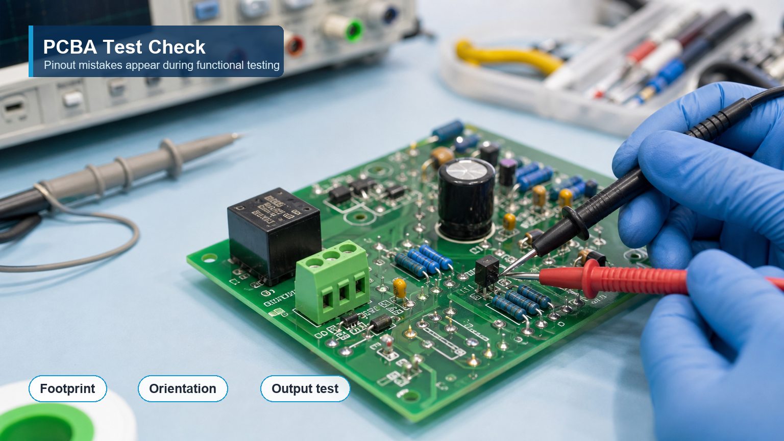
A small transistor can be difficult to inspect after it is surrounded by taller components, connectors, heatsinks, or enclosure hardware. Good layout and assembly planning make inspection and rework easier before the board reaches the final product stage.
2N2222 Pinout Project Example for a Small Control PCB
A practical 2N2222-related PCBA project may begin with a very simple request: “Please assemble this control board.” The real manufacturing risk appears when the BOM, footprint, and component supply are checked together.
A customer developing a small industrial control PCB needed a 2N2222-family transistor to drive a buzzer and an indicator output. The first sample quantity was 50 pieces for functional validation, followed by a planned small batch after enclosure testing. The board used FR4 material, mixed SMT and through-hole parts, terminal blocks, LEDs, and several discrete components.
Project details:
- Application: compact industrial control module
- Quantity: 50 prototype PCBAs before small-batch production
- Board type: FR4 PCB with mixed assembly
- Main component concern: 2N2222-family transistor availability and orientation
- Assembly needs: SMT placement, through-hole assembly, visual inspection, and functional test support
- Delivery focus: quick prototype build for circuit and enclosure validation
During file review, the schematic symbol looked correct, but the BOM used a supplier-specific 2N2222A part while the footprint appeared to be copied from another TO-92 transistor. The customer also allowed substitute parts if the original part was unavailable. That created a real risk: a substitute could meet the electrical requirement but use a different pin order or package drawing.
Main checks before production:
- Matched the BOM part number against the selected package drawing.
- Checked emitter, base, and collector mapping against the PCB pads.
- Flagged substitute approval as an engineering review item, not only a purchasing item.
- Confirmed the transistor orientation mark on the assembly drawing.
- Added functional test attention for the buzzer and indicator output.
This type of review does not change the customer’s circuit design. It protects the manufacturing result by making sure the approved design data, purchased component, PCB footprint, and assembly process all describe the same physical part.
For buyers, the value is practical: fewer assembly surprises, fewer emergency footprint corrections, and fewer delays between prototype validation and small-batch production.
FAQs About 2N2222 Pinout
Is the 2N2222 pinout always the same?
No. The pinout depends on the exact part number, package, manufacturer datasheet, and view direction. Always confirm the selected datasheet before PCB footprint release.
What are the three pins of a 2N2222 transistor?
The three terminals are emitter, base, and collector. Their physical order must be checked against the exact package drawing.
Is 2N2222A the same as PN2222A?
They are related NPN transistor options, but buyers should not assume identical package, pin order, or manufacturer specifications without datasheet review.
Can a wrong 2N2222 footprint cause PCBA failure?
Yes. A wrong footprint or reversed pin mapping can stop the transistor from switching correctly and may require rework or PCB revision.
Can EBest Circuit check 2N2222 orientation before assembly?
Yes. EBest Circuit can support PCB layout manufacturability review, BOM and footprint checks, PCBA assembly, inspection, and functional testing support based on customer-approved files.
In Conclusion, 2N2222 pinout affects more than a symbol on the schematic. It affects footprint selection, BOM substitution, silkscreen direction, soldering quality, inspection, and functional test results. Before PCB fabrication or PCBA assembly, confirm the exact datasheet, package, pin view, and assembly orientation.
EBest Circuit (Best Technology) supports PCB fabrication, PCB layout manufacturability review, component sourcing coordination, PCBA assembly, inspection, and testing support for transistor-based boards. For project review, send Gerber files, BOM, pick-and-place file, assembly drawing, and test requirements to sales@bestpcbs.com.