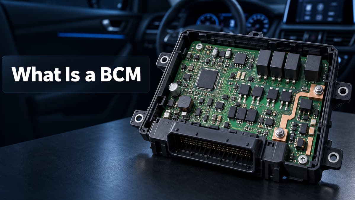
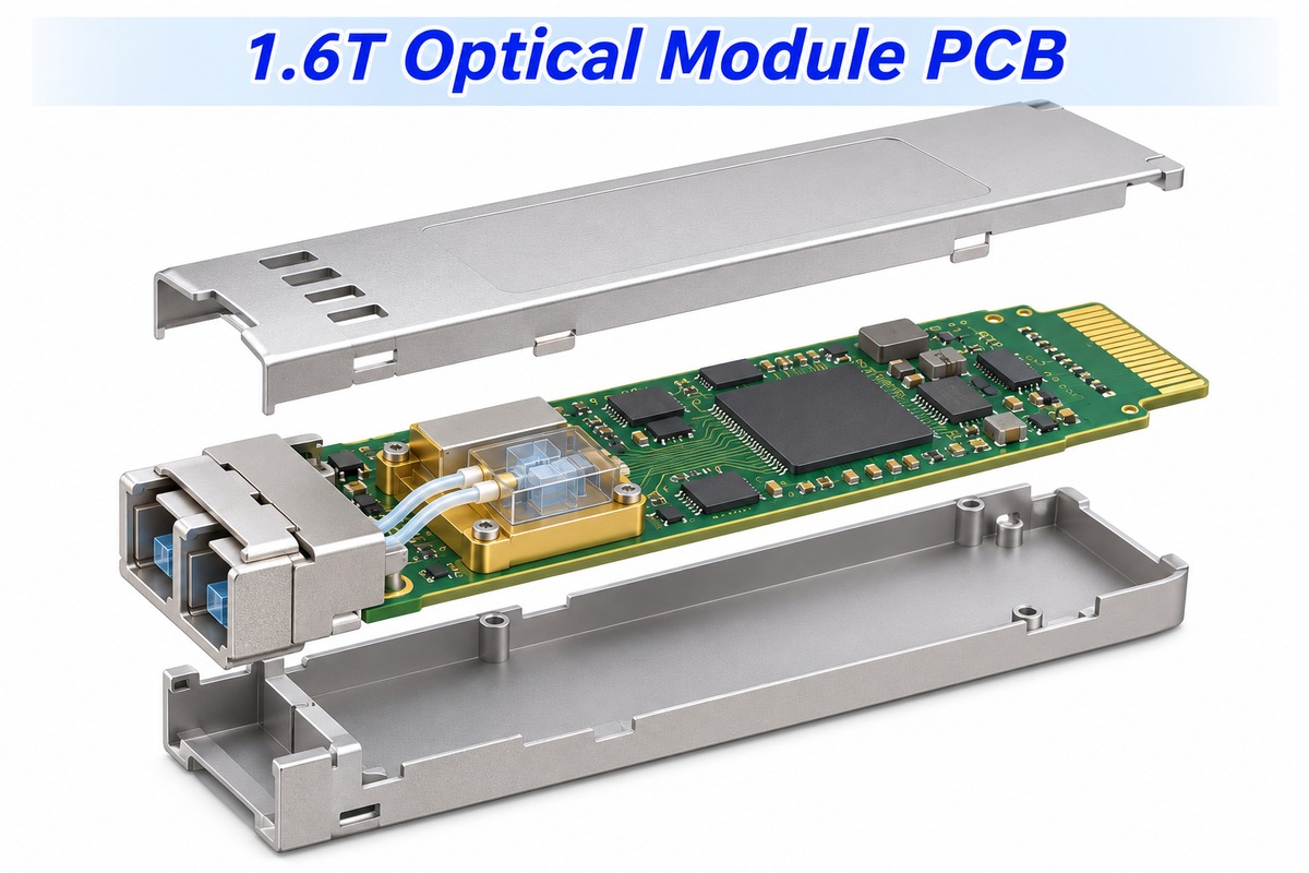
A 1.6T optical module PCB is the board inside a 1.6-terabit-per-second optical transceiver. It connects the module’s electrical contacts to the signal-processing and optical electronics, distributes power, and supports module control. The fiber and optics carry light; the PCB carries electrical signals.
The layout starts with the module architecture. A 1.6T OSFP module can use eight host electrical lanes in the 200 Gb/s class. Where those lanes terminate, how the optical engine connects, and how heat reaches the case all affect where parts and traces can fit.
Key Takeaways
- The module PCB is the electrical interconnect inside the transceiver, not the switch host board or the optical engine itself.
- Eight 200 Gb/s-class host lanes are one 1.6T implementation. The aggregate rate alone does not specify either the electrical interface or the optical format.
- Design the edge contacts, trace fanout and first layer transition as one launch. Check connector and board dimensions together.
- Place voltage regulators and hot components with the enclosure and cooling design in view. A good electrical floorplan can still miss the thermal target.
- Separate bare-board acceptance, assembled electrical validation and optical compliance. Each answers a different question.
Why Are PCB Manufacturers Investing in High-Speed Optical Modules?
High-speed optical modules are one of the applications identified in Founder Technology’s November 13, 2026 investor-relations disclosure. The company said it planned to start trial production at its F8 plant by year-end, with the 2027 production ramp focused in part on high-speed optical modules. The disclosure does not establish a particular 1.6T module stackup or a universal laminate requirement.
Before you finalize the layout, we can review the module’s edge contacts and first via transition against the proposed stackup. That’s where a controlled-impedance PCB can still run into reflections, even when the straight traces meet their impedance target.
What Is Inside a 1.6T Optical Transceiver?
A DSP-based 1.6T optical transceiver architecture has a host electrical interface, a digital signal processor, transmit and receive optics, and support circuits for power and management. On transmit, the DSP processes the incoming electrical lanes, and a driver feeds the optical transmitter or modulator. On receive, a photodetector and transimpedance amplifier produce an electrical signal for the receive chain.
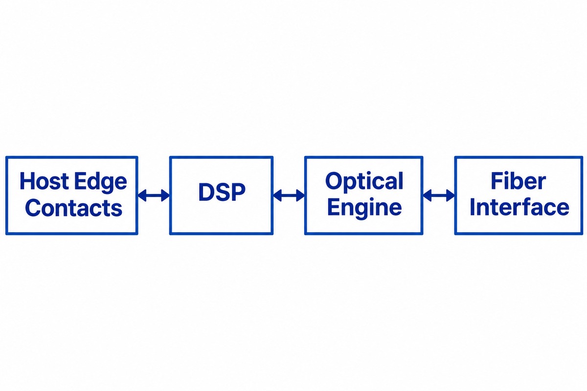
The optical engine may integrate several of these functions. Its physical connection to the board depends on the package and module architecture. A module without a full retiming DSP will not follow the same block diagram, so use the selected device documentation rather than assuming all 1.6T modules have the same parts.
How Do Host Electrical Lanes Differ from Optical Lanes?
Host lanes are electrical connections at the module edge. Optical lanes describe how the module sends light over fibers or wavelengths. An eight-lane host interface does not, by itself, identify the optical connector or the number of fibers.
| Interface | Example 1.6T host electrical configuration |
|---|---|
| OSFP | 8 × 200 Gb/s class |
| QSFP-DD1600 | 8 × 200 Gb/s class |
| OSFP-XD, 16-lane mode | 16 × 100 Gb/s class |
The term “1.6T OSFP 224” refers to the 224 Gb/s-class electrical signaling capability, not a claim that the application delivers 224 Gb/s of payload per lane. For example, the OSFP-XD MSA specifies 106.25 GBd for its 1.6TAUI-8 mode under that signaling class. Model the rate specified for the selected interface rather than using the class label as the exact symbol rate.
What Makes the Edge Launch Difficult on a 1.6T Optical Module PCB?
The transition from the host connector to the PCB trace has several geometry changes in a short distance. Contact-pad length, the trace neckdown, the reference plane beneath the pads and the first via can all affect reflections. QSFP-DD MSA Rev. 7.1 gives tighter tolerances for specific QSFP-DD1600 paddle-card contact dimensions; use the applicable drawing rather than applying those dimensions to OSFP.
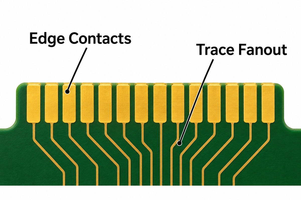
Model the launch before locking the stackup. A coupon can verify a uniform differential pair, but it cannot reproduce the connector transition unless the test structure includes that transition. Keep the proposed dielectric thickness, copper foil and actual fabrication geometry with the model. See our high-speed PCB materials guide for the material variables that affect loss.
How Does a 1.6T Optical Module PCB Distribute Power?
A 1.6T optical module PCB routes the module supply to local regulators, then distributes the regulated rails to the DSP, optical electronics and control circuits. A total wattage does not tell you how to size one rail. Start with each device’s voltage, steady and transient current, allowed ripple and startup sequence.
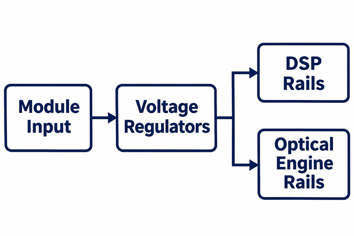
Keep high-current loops compact and give sensitive receive circuitry a planned supply path. Check the voltage at the load during startup and operating mode changes, not only at the regulator output. A rail that measures correctly at idle can still dip when processing or optical circuits turn on.
How Does the Enclosure Shape a 1.6T Optical Module PCB?
The case and cooling hardware determine where heat can leave the PCB assembly. A common path takes heat from the DSP package through a thermal interface pad to the metal housing. From there, the cage, heatsink and airflow determine how effectively the system removes it.
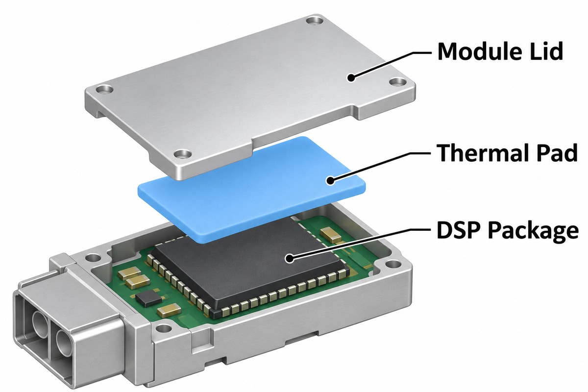
For 1.6T optical transceiver power consumption, use the selected module’s rating and operating conditions. Do not treat the entire module power as heat from one chip. Check component height and pad compression against the tolerance stack. A gap to the lid or a poorly compressed pad can raise package temperature even when the airflow is unchanged.
What Should You Verify Before Approving the Board?
For a 1.6T optical module PCB, verify the bare-board geometry, the assembled electrical path and the completed module separately. That makes it easier to tell whether a fault comes from the PCB, assembly, optical engine or cooling setup.
- Bare PCB: Check finished board thickness, edge contacts, stackup and representative impedance or loss coupons against the drawing.
- Assembled board: Check startup sequencing, rail behavior at the load and electrical path measurements at the intended reference planes.
- Finished module: Validate optical performance and link errors under the specified conditions, including case temperature and representative airflow.
FAQ About 1.6T Optical Module PCBs
Does a 1.6T optical module PCB have to use M9 material?
No. The interface specification does not prescribe one laminate grade. Choose materials against the channel budget, routing geometry, foil roughness and the fabricator’s proposed construction. Verify the result on a representative test structure.
Can I copy an edge-contact footprint from another module family?
Not without checking the applicable drawing. Contact dimensions, thickness, tolerances and connector engagement are part of the interface. Similar-looking contacts do not establish mechanical fit or electrical performance.
Does a linear pluggable module eliminate all signal processing?
No. A linear pluggable architecture moves more equalization responsibility to the host and omits the conventional module retiming DSP. The module still contains electronics for driving the transmitter and receiving signals from the photodetector.
Does the PCB have a fixed layer count?
No. Layer count depends on package escape, routing capacity, reference-plane continuity, power distribution and the allowed finished thickness. The same module rate does not make different layouts interchangeable.
Can I test a module outside its cage?
Yes for initial checks, but a bench test does not reproduce the installed thermal conditions. Verify temperature and link performance with the cage, heatsink and airflow specified for the application.
What Should You Send for a Board-Level Review?
Send the board outline, connector drawing, target stackup, critical lane geometry and mechanical height limits to sales@bestpcbs.com. If the review includes PCB assembly, include the BOM and any special requirements for the optical-engine package or thermal interface.