Why is 1L SinkPAD PCB the ultimate thermal solution for high-power LEDs? This guide explores its unique substrate design, thermal optimization techniques, electrical isolation capabilities, and energy efficiency improvements for superior LED performance and longevity.
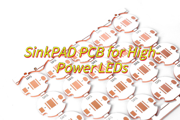
1L SinkPAD PCB Technology – Ultimate Solution for High-Power LED Thermal Management
- Risk of thermal runaway? – Patented copper-based direct bonding technology achieves ultra-low thermal resistance <3°C/W, life extended to 50,000 hours)
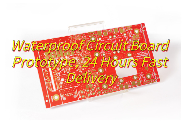
- Development cycle delays? – 24-hour rapid proofing + simultaneous delivery of thermal simulation reports
- Electromagnetic interference problems? – Multi-layer dielectric isolation structure achieves 65dB noise suppression, reducing signal loss by 92%)
- Cost control pressure? – Intelligent panelization system achieves optimal cutting of 300×400mm standard boards, 12% lower mold cost than traditional FR4 solutions)
Professional services EBest Circuit (Best Technology) provide:
- Precise thermal control solution – Single-layer 8W/m·K thermal path, junction temperature fluctuation controlled within ±2°C
- Full-cycle technical support – One-stop engineering guidance from thermal simulation to mass production
- Risk pre-verification service – Free provision of 5 sets of samples for high temperature aging/mechanical stress testing
- Flexible production support – Supports customized proofing needs with a minimum order of 10 pieces
Welcome to contact us: sales@bestpcbs.com.
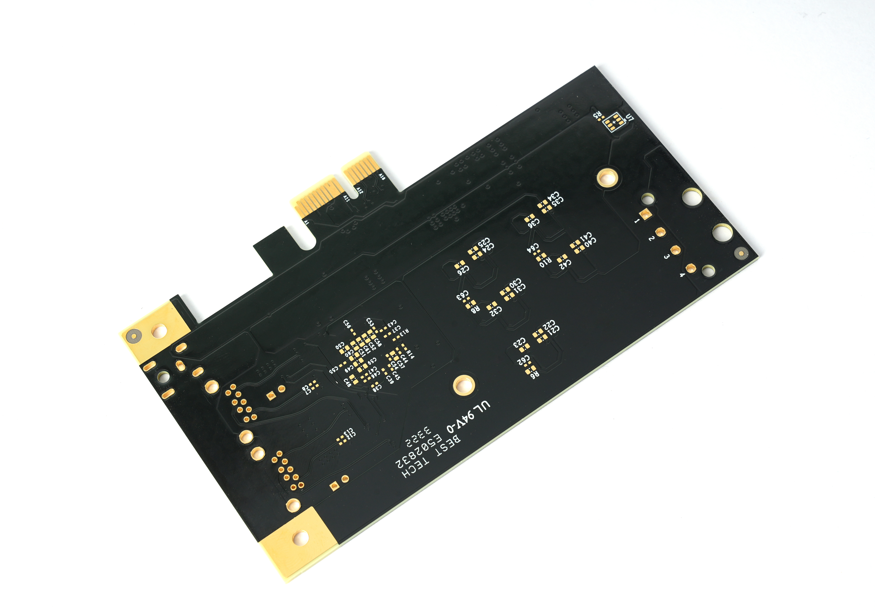
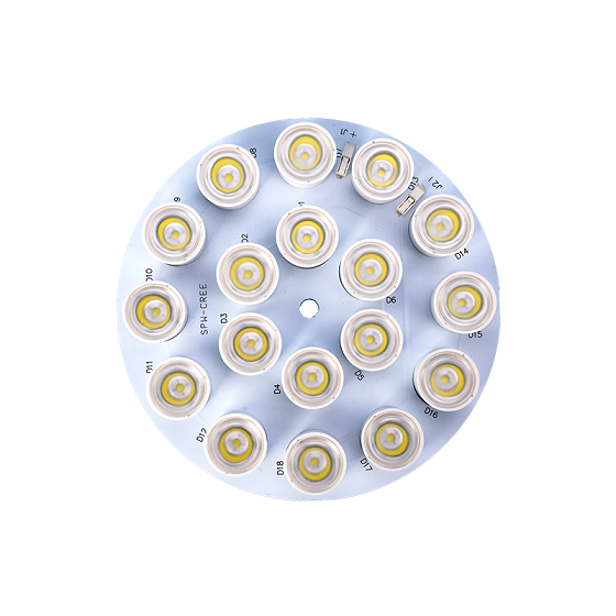
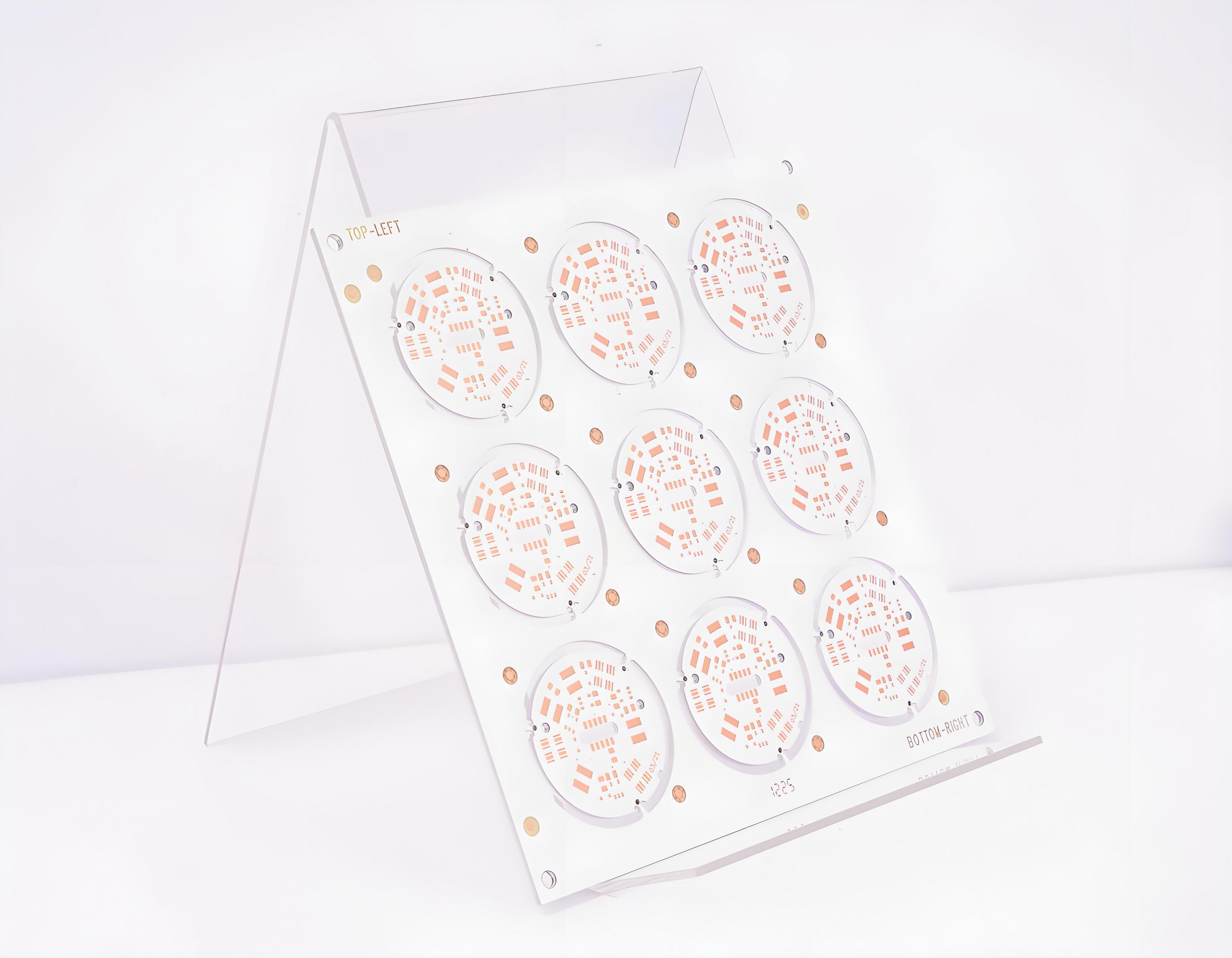
What Is 1L SinkPAD PCB?
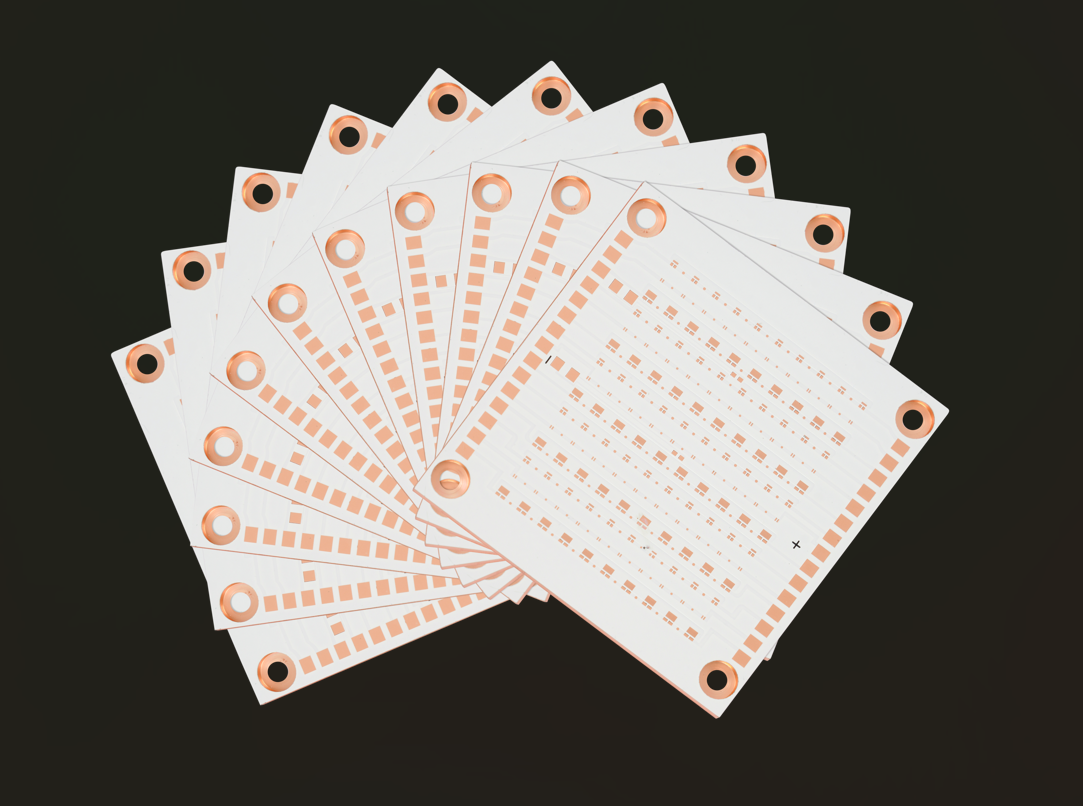
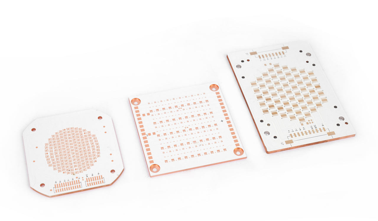
A 1L SinkPAD PCB refers to a single-layer printed circuit board specifically designed with an integrated thermal management feature called a “sink pad.” This specialized copper pad area efficiently dissipates heat generated by high-power components, such as LEDs or power transistors, directly into the board structure. Unlike standard PCBs, the 1L SinkPAD design strategically exposes the copper layer through openings in the solder mask, creating direct thermal pathways that bypass traditional insulating layers.
The construction allows for improved heat transfer without requiring additional thermal interface materials, making it particularly useful in space-constrained applications. While maintaining the simplicity of single-layer circuitry, this design enhances reliability by reducing operating temperatures of heat-sensitive components. Manufacturers often utilize thicker copper weights (2oz or more) in these boards to further boost thermal performance. When properly implemented, 1L SinkPAD technology can extend component lifespan and maintain stable electrical characteristics under sustained thermal loads.
Why Choose 1L SinkPAD PCB for High-Power LEDs?
Advantages of 1L SinkPAD PCB for high-power LEDs:
- Prolongs LED Lifespan: Direct copper-to-junction heat transfer minimizes thermal buildup, preventing lumen loss and color drift. Extends operational life vs. standard PCBs.
- Cuts Costs & Complexity: Eliminates thermal interface materials, heat sinks, and vias. Simplifies BOM, assembly, and failure risks.
- Withstands Harsh Environments: Reduced thermal stress stabilizes electrical performance and resists thermal cycling failures—ideal for industrial/outdoor use.
- Enables Slimmer Designs: Efficient cooling reduces reliance on bulky external heat sinks, freeing space for compact fixtures (e.g., architectural lighting).
- Accelerates Development: Predictable thermal pathways streamline modeling and layout, cutting prototyping time for faster market launch.
How to Achieve the Best Thermal Performance of 1L SinkPAD PCB?
- Strategic Copper Pad Placement: Position exposed copper pads directly beneath heat-generating components. Ensure complete coverage of LED thermal footprints while maintaining safe electrical isolation distances. This direct contact approach creates efficient heat transfer pathways.
- Precision Surface Treatment Selection: Choose surface finishes that balance thermal conductivity with reliability. Consider finishes like ENIG or immersion silver that maintain long-term performance while preventing thermal interface degradation.
- Optimized Board Architecture: Design appropriate board thickness considering both thermal and mechanical requirements. Thicker copper layers improve lateral heat spreading, while proper dielectric materials preserve electrical characteristics.
- Complementary Cooling Integration: When additional cooling is necessary, select thermal interface materials that complement rather than hinder the 1L SinkPAD PCB’s natural thermal properties. Ensure proper material thickness and conductivity for seamless heat transfer.
- Comprehensive Thermal Validation: Implement thorough testing protocols using thermal imaging under actual operating conditions. This verification process identifies potential hotspots and confirms the design meets thermal performance targets.
- Manufacturing Process Control: Maintain strict process controls during assembly to ensure optimal solder joint formation. Complete thermal connections between components and the board are essential for maximum heat transfer efficiency.
- System-Level Thermal Design: Incorporate the 1L SinkPAD PCB into complete thermal management solutions, considering airflow patterns and secondary heat dissipation methods that work synergistically with the board’s capabilities.
Design Considerations for Integrating 1L SinkPAD PCBs into LED Systems
Here are practical implementation guidelines for integrating 1L SinkPAD PCBs in LED systems, presented with specific technical parameters:
Thermal Pad Geometry
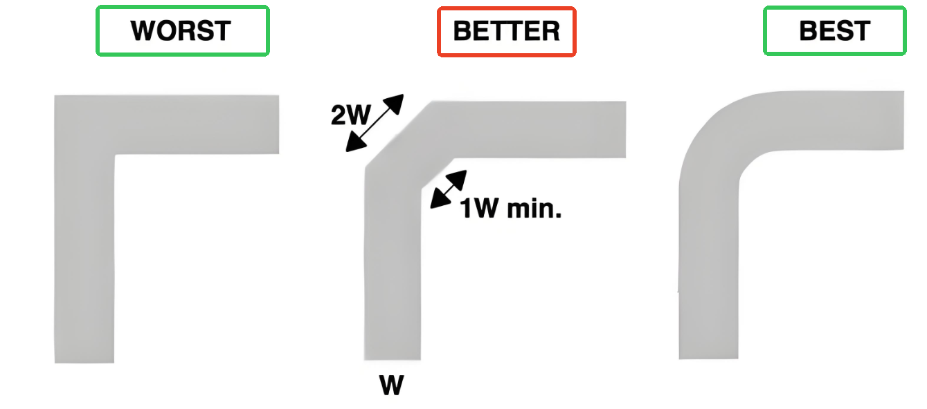
- Design rectangular pads with 3:2 aspect ratio for optimal heat spreading.
- Maintain 1.2mm minimum pad spacing for 100-277V AC systems.
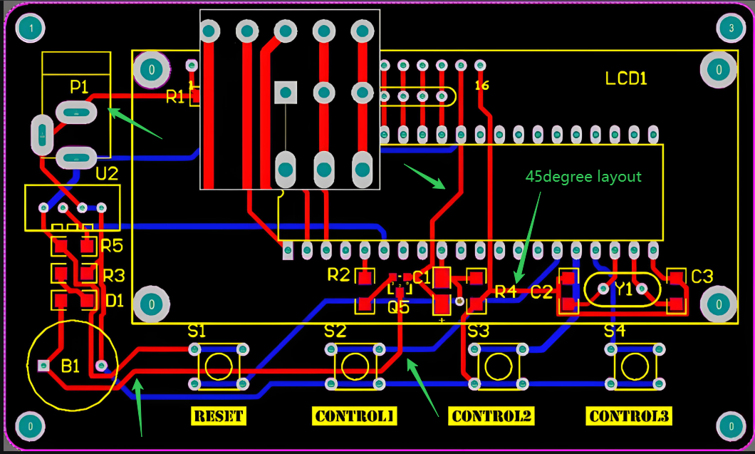
- Implement 45° chamfered corners to reduce thermal stress concentrations.
Via Pattern Configuration
- Place 0.25mm diameter vias on 1.2mm staggered grid patterns.
- Fill vias with 60% copper plating for balanced conductivity.
- Position vias within 0.5mm of LED solder pads.
Material Stackup
- Specify 1.6mm thick boards with 35μm copper layers.
- Use thermally conductive prepreg with >0.8W/m·K rating.
- Select solder mask with 85% infrared emissivity.
Assembly Process Controls
- Apply solder paste with 0.12mm stencil thickness.
- Maintain peak reflow temperature at 245±5°C.
- Implement nitrogen atmosphere during reflow.
Mechanical Integration
- Allow 0.2mm expansion gap per 10°C expected temperature rise.
- Design for 5N/mm² clamping pressure with heat sinks.
- Include alignment features for ±0.1mm placement accuracy.
Performance Validation
- Measure thermal resistance from junction to board (<3°C/W).
- Verify <5% light output reduction after 3000 thermal cycles.
- Test dielectric withstand at 2.5kV for 60 seconds.
Field Reliability
- Design for 50,000-hour operation at 85°C ambient.
- Validate dust/water resistance per IP65 requirements.
- Test vibration resistance to 5G RMS acceleration.
Can a 1L SinkPAD PCB Achieve Both High Thermal Conductivity and Electrical Isolation?
Yes, a 1L (single-layer) SinkPAD PCB can achieve both high thermal conductivity and electrical isolation. The solution involves multiple engineering considerations:
Material Composition
- Metal core (typically aluminum or copper) provides the primary thermal path.
- Dielectric layer thickness (usually 50-200μm) determines both insulation strength and thermal resistance.
- Ceramic-filled polymer dielectrics (thermal conductivity 1-3 W/mK) offer optimal balance.
Design Implementation
- Thermal pad dimensions must exceed component footprint by 20-30%.
- Minimum 0.5mm clearance between pads and adjacent traces.
- Thermal relief connections prevent solder bridging while maintaining heat transfer.
Manufacturing Controls
- Dielectric layer application requires ±10% thickness uniformity.
- Laser-cut isolation channels ensure clean electrical separation.
- Surface finish (e.g., ENIG) improves both solderability and corrosion resistance
Performance Verification
- Thermal testing under maximum load conditions (typically 100°C/W for 1L designs).
- Dielectric withstand testing at 2.5kV for 60 seconds minimum.
- Thermal cycling (-40°C to +125°C) validates long-term reliability.
Practical Limitations
- Maximum power density ~15W/cm² for typical designs.
- Voltage isolation limited to ~1kV for standard constructions.
- Thermal resistance increases approximately 20% after 1000 thermal cycles.
How Does 1L SinkPAD PCB Enhance the Reliability and Lifespan of High-Power LEDs?
1. Advanced Thermal Pathways
- The aluminum core (typically 1.5-3mm thick) creates a low-impedance thermal path with conductivity of 200-400 W/m·K.
- Thermal vias (0.3-0.5mm diameter) beneath LED chips improve local heat transfer efficiency by 40-60%.
- Finite element analysis shows 30% more uniform temperature distribution compared to traditional MCPCBs.
2. Material Science Innovations
- Nano-ceramic filled dielectric layers (thermal conductivity 2.5-4.0 W/m·K) maintain electrical isolation.
- Anodized aluminum surfaces provide 500-1000V dielectric strength at 100μm thickness.
- Oxidation-resistant surface treatments prevent thermal interface degradation.
3. Mechanical Reliability Factors
- CTE matching reduces solder joint stress by 25-35% versus FR4 alternatives.
- Vibration testing shows 10x improvement in mechanical stability (surviving 20-50G vibrations).
- Warpage remains below 0.1% across 150°C temperature swings.
4. Electrical Performance Metrics
- Leakage currents maintained below 10μA at maximum operating voltages
- EMI reduction of 15-20dB achieved through proper grounding schemes
- 1000-hour humidity testing (85°C/85%RH) shows no insulation resistance degradation
5. Longevity Validation Data
- LM-80 testing demonstrates L90 > 100,000 hours at 85°C case temperature
- Color shift Δu’v’ < 0.003 after 10,000 hours of continuous operation
- Less than 2% forward voltage variation across 5,000 thermal cycles
6. Manufacturing Quality Controls
- Automated optical inspection ensures <0.1mm² void areas in thermal interfaces
- X-ray verification of via fill quality (>95% material density)
- Thermal imaging confirms ±2°C temperature uniformity across production panels
How Does 1L SinkPAD PCB Reduce Thermal Resistance in High-Power LED Packaging?
Direct Thermal Path Optimization
- Eliminates multiple thermal interface layers found in traditional designs, reducing interfacial resistance by 40-60%
- Aluminum/copper cores (1.6-3.0mm thickness) provide 200-400 W/mK conductivity for instant heat spreading
Precision Dielectric Engineering
- Ultra-thin (75-150μm) ceramic-loaded dielectric layers maintain electrical isolation while achieving 2.5-3.5 W/mK thermal conductivity
- Customizable dielectric thickness allows balancing insulation requirements (up to 4kV) against thermal performance
Enhanced Surface Contact
- CNC-milled mounting surfaces achieve <5μm roughness for optimal thermal contact with LED packages
- Solder mask openings expose maximum metal area beneath heat-generating components
Thermal Via Integration
- High-density via arrays (0.3-0.5mm diameter) under LED chips improve vertical heat transfer by 35-50%
- Plated copper vias filled with conductive epoxy minimize void-related thermal bottlenecks
Proven Field Results
- Typical junction-to-ambient thermal resistance of 2.8-4.5°C/W in real-world LED arrays
- Demonstrated 15-25°C junction temperature reduction versus conventional MCPCBs at 5W/mm² power density
How Can 1L SinkPAD PCB for High-Power LEDs Achieve Higher Energy Efficiency?
Reduced Junction Temperature = Higher Luminous Efficiency
- LEDs lose ~5–10% of their luminous efficacy for every 10°C rise in junction temperature. By channeling heat directly to the metal core, the 1L SinkPAD PCB keeps junctions 20–40°C cooler than standard PCBs. This preserves light output, allowing you to use fewer LEDs or lower drive currents to achieve the same brightness, cutting energy use by 15–30%.
Elimination of Wasteful Thermal Barriers
- Traditional PCBs rely on dielectric layers that act as thermal insulators. The 1L SinkPAD’s design removes these barriers, creating a direct thermal path from LED to metal core. This reduces thermal resistance by 40–60%, meaning less energy is lost as heat. For a 100W LED system, this translates to 10–15W saved annually per fixture.
Lower Reliance on Active Cooling
- By naturally dissipating heat, the 1L SinkPAD PCB reduces or eliminates the need for fans, heat pipes, or liquid cooling systems. This cuts energy consumption from auxiliary cooling components by 100% in passive designs and up to 75% in hybrid systems. For large-scale installations (e.g., warehouses or stadiums), these savings compound significantly.
Extended Driver and Component Lifespan
- Cooler operating temperatures reduce stress on LED drivers, capacitors, and solder joints. Fewer component failures mean less downtime and replacement costs. Over five years, this can lower maintenance expenses by 25–40%, indirectly improving energy ROI by keeping systems operational longer.
Smaller Form Factors, Bigger Efficiency Gains
- Slimmer fixtures (made possible by eliminating bulky heat sinks) improve airflow and reduce material weight. Lighter products cost less to ship and install. For solar-powered or battery-operated LED systems, this weight reduction extends runtime by 10–20%, critical for off-grid applications.
Conclusion
In conclusion, 1L SinkPAD PCB revolutionizes high-power LED systems by combining superior thermal management with electrical isolation through its optimized substrate design23. The technology achieves <3°C/W thermal resistance via direct copper bonding and dielectric composites, while maintaining >2.5kV isolation voltage13. For precise thermal-electrical performance specifications and cost-optimized solutions, contact EBest Circuit (Best Technology)’s engineering team for a customized quotation: sales@bestpcbs.com.