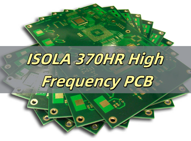
Rogers RO4350B is one of the most popular PCB materials used in high-frequency applications today. If you’re designing circuits that need stable performance at GHz-level speeds, this material often stands out. In this blog, we’ll explore what RO4350B is, what it’s made of, available thicknesses, and why it’s preferred over other materials for high-frequency PCB designs.
What Is Rogers RO4350B Material?
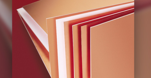
RO4350B is a type of high-frequency laminate developed by Rogers Corporation. It’s engineered for performance in RF (radio frequency) and microwave applications, offering superior electrical characteristics compared to standard FR-4. Unlike generic epoxy-based materials, RO4350B uses a hydrocarbon-ceramic composition that keeps signal losses low even at high frequencies.
This material combines the electrical performance of PTFE (commonly used in high-end RF applications) with the manufacturability of FR-4, making it a cost-effective and reliable choice for high-speed designs.
What Is Rogers Material Made of?
Rogers materials, including RO4350B, are made from hydrocarbon resins with ceramic fillers and reinforced with woven glass. This composite structure delivers excellent mechanical stability and consistent dielectric properties.
Unlike traditional PTFE-based laminates, Rogers materials like RO4350B do not require special handling during PCB fabrication, which saves both time and cost. Rogers materials are engineered to balance electrical performance with ease of manufacturing, which is essential when producing high-frequency PCBs at scale.
RO4350B Dielectric Constant
The dielectric constant (Dk) is a critical factor in high-frequency PCB materials, as it affects signal speed and impedance control. The RO4350B dielectric constant is typically 3.48 ± 0.05 at 10 GHz, which is both stable and predictable over a wide range of frequencies and temperatures.
The consistency of frequencies and temperatures ensure that transmission lines behave as expected, which is especially important in RF circuits, microwave devices, and antenna structures. Stable Dk also simplifies impedance control and reduces the risk of signal reflection and distortion.
What Is the Standard RO4350B Thickness?
RO4350B PCBs are available in multiple standard thicknesses to meet different design and performance requirements. Common options include:
- 0.254 mm (10 mil)
- 0.508 mm (20 mil)
- 0.762 mm (30 mil)
- 1.524 mm (60 mil)
These thicknesses allow designers to select the best stack-up for impedance control, thermal dissipation, and mechanical strength. Depending on your signal layer, ground layer spacing, or copper weight, one of these thicknesses will likely align with your project’s needs.
RO4350B Datasheet
Before choosing a material for your RF or high-speed digital PCB, it’s essential to understand the technical specifications. Here is a summary of the most important values from the RO4350B datasheet:
| Property | Typical Value | Test Condition / Note |
| Dielectric Constant (Dk) | 3.48 ± 0.05 | @ 10 GHz (z-axis) |
| Dissipation Factor (Df) | 0.0037 | @ 10 GHz |
| Volume Resistivity | 1.7 × 10⁸ MΩ·cm | ASTM D257 |
| Surface Resistivity | 4.4 × 10⁷ MΩ | ASTM D257 |
| Electrical Strength | >800 V/mil | ASTM D149 |
| Dielectric Breakdown | >40 kV | ASTM D149 |
| Thermal Conductivity | 0.69 W/m·K | ASTM D5470 |
| Coefficient of Thermal Expansion (CTE) | 11 ppm/°C (x, y) / 32 ppm/°C (z) | -55°C to 288°C |
| Glass Transition Temperature (Tg) | >280°C (no defined Tg) | Thermomechanical analysis |
| Decomposition Temperature (Td) | ~425°C | TGA method |
| Solder Reflow Resistance | Excellent | No delamination or blistering |
| Tensile Modulus | 1.4 × 10⁶ psi (x-y) | ASTM D638 |
| Flexural Strength | 20,000 psi (typical) | ASTM D790 |
| Peel Strength | ≥1.1 N/mm | IPC-TM-650 |
| Young’s Modulus | ~10 GPa | Estimated from stress-strain curve |
| Moisture Absorption | 0.06% | ASTM D570 |
| Density | 1.86 g/cm³ | ASTM D792 |
| Flammability Rating | UL 94 V-0 | UL 94 |
| Water Absorption | <0.1% | Excellent water resistance |
| Material Composition | Ceramic-filled hydrocarbon resin + glass fiber | Non-PTFE-based |
| Halogen-Free | Yes | RoHS & REACH compliant |
| Available Copper Foil | 0.5 oz, 1 oz, 2 oz (18µm, 35µm, 70µm) | Rolled and electro-deposited options available |
If you need the full official datasheet in PDF format, you can also request it from EBest Circuit (Best Technology) along with a quote for your project.
How Much Does Rogers PCB Cost?
Compared to FR-4, the rogers RO4350B price is higher due to its premium performance. On average, RO4350B material can cost between $8 to $25 per square foot, depending on thickness, copper weight, and supplier volume. Full PCB fabrication using RO4350B typically results in a 20–50% higher price than using standard FR-4, mainly due to the material cost and additional processing steps.
However, when you’re working with high-frequency applications—such as 5G, radar, or satellite communications—the improved signal integrity and reduced loss often justify the added cost.
What Is the Difference Between RO4003 and RO4350B?
Both RO4003 and RO4350B are part of Rogers’ high-frequency laminate series, but they have subtle differences:
| Feature | RO4003C | RO4350B |
| Dielectric Constant | 3.38 | 3.48 |
| Loss Tangent | 0.0027 @ 10 GHz | 0.0037 @ 10 GHz |
| Flame Rating | Non-UL rated | UL 94 V-0 |
| Cost | Slightly lower | Slightly higher |
| Process Compatibility | Standard PCB process | Standard PCB process |
RO4003 is better suited for applications where cost sensitivity is critical and UL rating is not required. RO4350B, on the other hand, provides a better flame rating and slightly improved mechanical properties, so it is the preferred choice for commercial or defense-grade applications.
Why Choose RO4350B as High Frequency PCB Material?
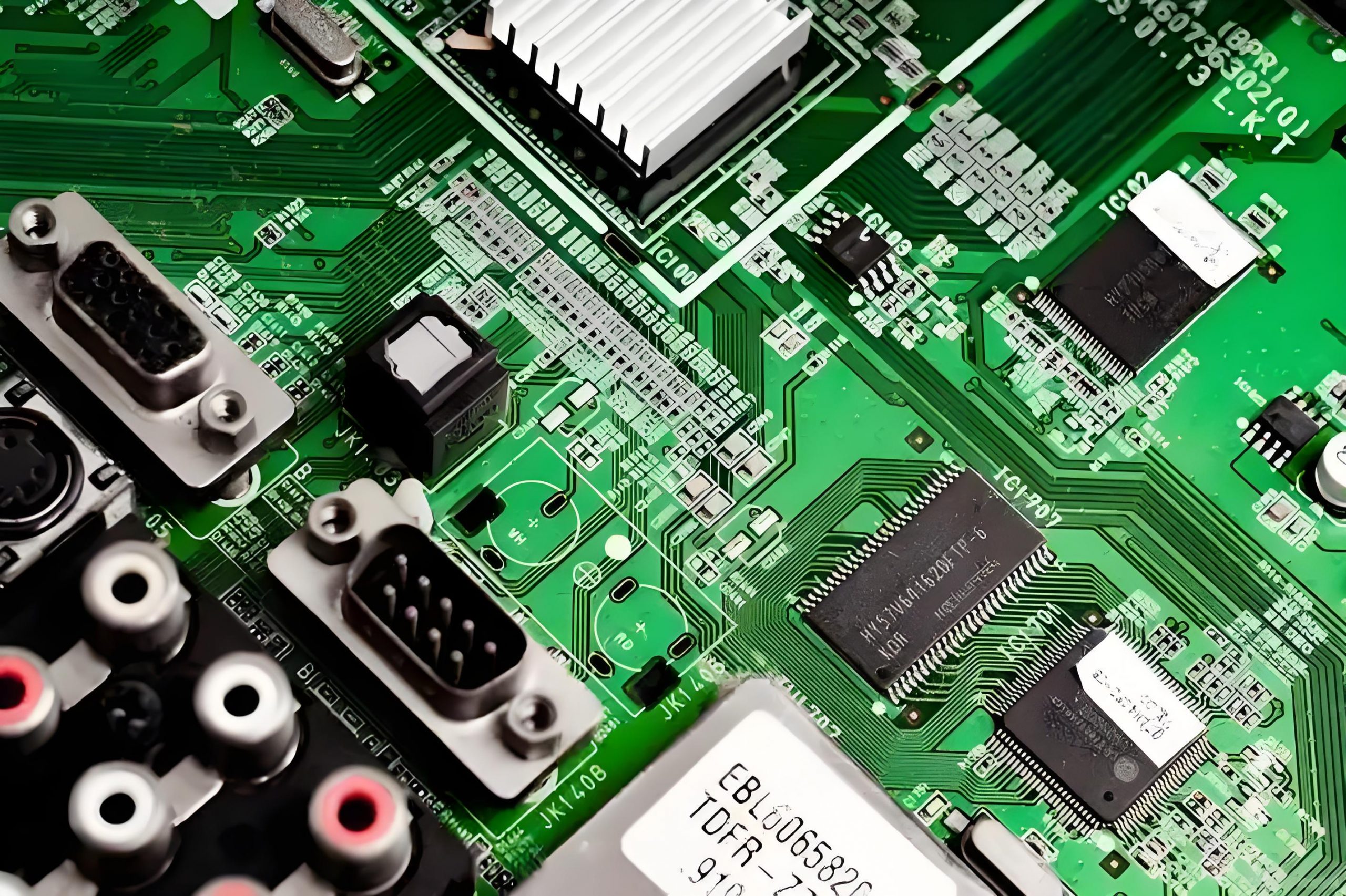
High frequency PCB, also known as RF PCB, refers to a special circuit boards with relatively high electromagnetic frequencies. This PCB is mainly used in the fields of high frequency (>300 MHz or wavelengths <=1 meter) and microwaves (>3 GHz or wavelengths <= 0.1 meter). If you’re designing a high-frequency PCB, choosing RO4350B gives you the best of both worlds: high performance and ease of fabrication. Here’s why many engineers choose this material:
- Low dielectric loss helps reduce signal attenuation.
- Stable dielectric constant ensures consistent impedance.
- Better thermal management compared to FR-4.
- UL 94 V-0 flame resistance, which is crucial for safety.
- Compatible with standard FR-4 processing, so no need for Teflon-specific tooling.
All of these feature help maintain signal quality in applications like RF transmitters, satellite receivers, and high-speed digital circuits. So even if the RO4350B price is slightly higher, it’s often more cost-effective than debugging performance issues caused by suboptimal materials.
High Frequency PCB Design Guidelines
When working with RO4350B PCB material, keep the following design practices in mind to get the best results:
1. Control impedance: Use proper stack-up and trace width calculators for accurate 50Ω or 75Ω routing.
2. Minimize vias: Each via introduces inductance and can distort signals at high frequencies.
3. Short trace lengths: High-speed signals should have the shortest possible paths.
4. Proper grounding: Always include a continuous ground plane to reduce EMI and improve return paths.
5. Avoid sharp corners: Use 45-degree or curved traces instead of 90-degree angles.
6. Use differential pairs: For high-speed interfaces like USB or LVDS, tightly coupled pairs reduce crosstalk and maintain signal integrity.
Combining these techniques with the natural performance of RO4350B helps you unlock superior RF performance without increasing fabrication complexity.
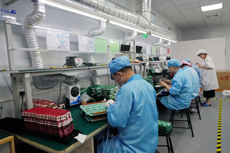
Why EBest Circuit (Best Technology) Is Your Reliable RF PCB Manufacturer?
At EBest Circuit (Best Technology), we specialize in high-frequency PCB manufacturing using premium materials like RO4350B, RO5880, RO4003C. With ISO-certifications, we’re equipped to serve industries ranging from automotive and medical to aerospace and communications. Whether you’re developing high-reliability prototypes or large-scale production, you can count on us as your reliable one-stop PCB & PCBA partner.
We offer:
- Strict impedance control with advanced test equipment
- Rapid prototyping and flexible volume production
- Competitive RO4350B price with guaranteed traceability
- Expert engineering support for layout and material selection
- No MOQ requires, 1 piece available also
- 5 years quality guarantee, free rework and functional testing
- Free DFM check
If you’re looking to manufacture reliable high-frequency PCBs, you’re in the right place.
FAQs
1. Is RO4350B suitable for multilayer PCBs?
Yes, RO4350B is commonly used in multilayer designs for RF and microwave applications. It offers stable performance in both single and multi-layer stack-ups.
2. How does RO4350B perform at 5GHz or higher?
It maintains low loss and consistent Dk values even at frequencies above 5GHz, making it reliable for 5G and radar circuits.
3. Can RO4350B be used with FR-4 in hybrid stack-ups?
Yes, it can. Many engineers use RO4350B for RF layers and FR-4 for power/control layers to reduce cost.
4. What is the shelf life of RO4350B material?
Stored under proper conditions, it has a long shelf life—typically over a year without degradation.
5. Do I need special PCB fabrication for RO4350B?
No. Unlike PTFE-based materials, RO4350B is compatible with standard PCB fabrication processes, which simplifies manufacturing.
Contact EBest Circuit (Best Technology) today to get a quote or talk with our engineers about your RF design needs.