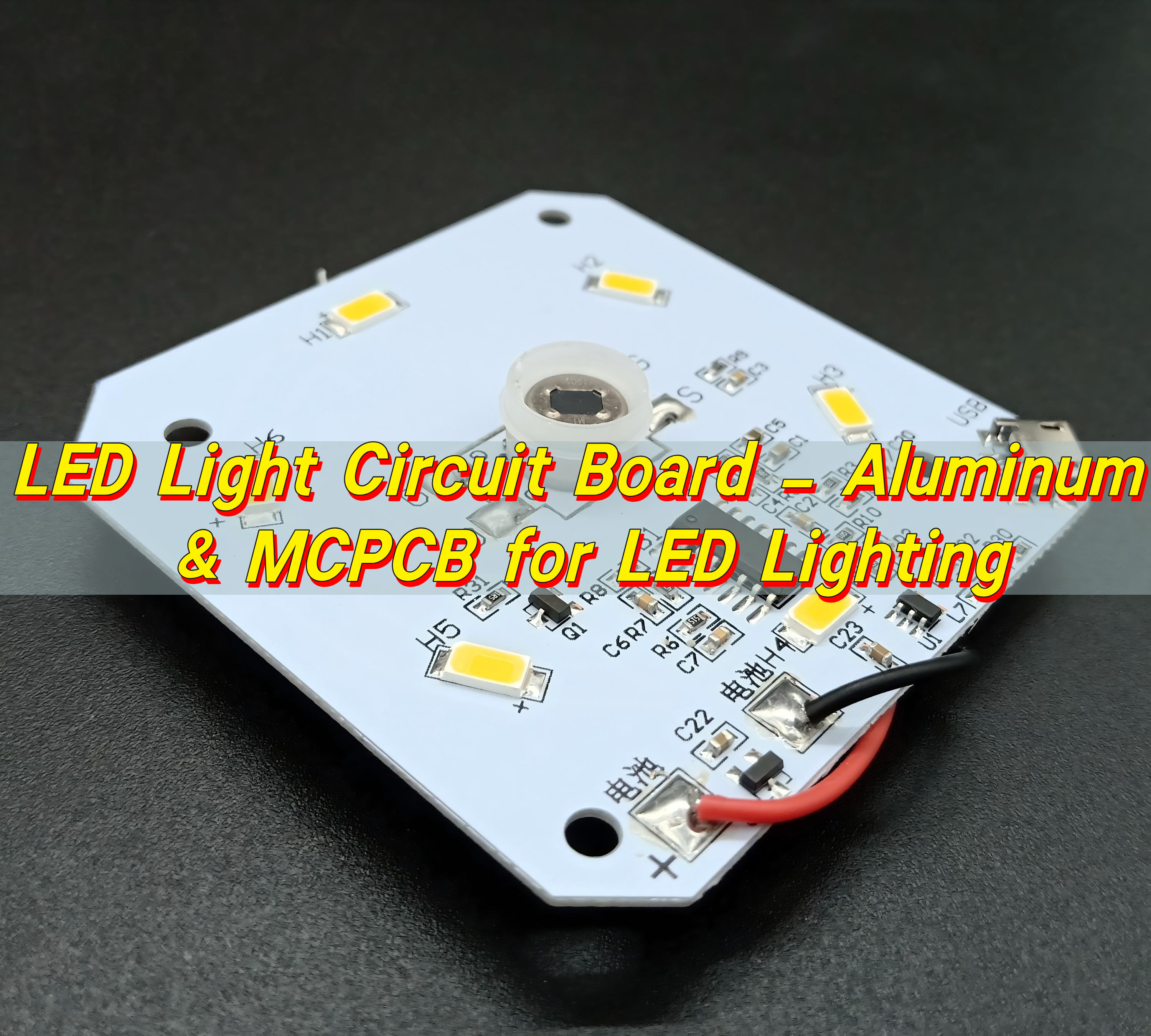
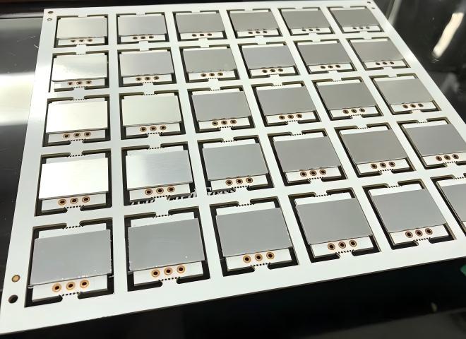
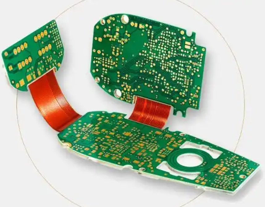
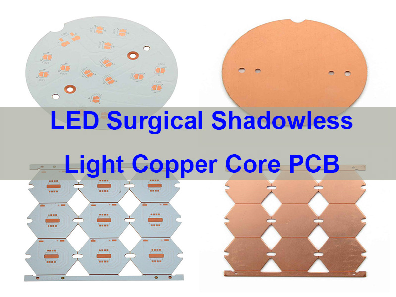
LED surgical shadowless light copper core PCB is the thermal backbone of modern operating room lighting, ensuring stable lumen output, uniform illumination, and long service life under continuous high-power operation.
Key Parameters You Should Care About
- Thermal conductivity: ≥ 380 W/m·K (pure copper core)
- Copper thickness: 1–4 oz (customizable)
- Dielectric thickness: 50–150 μm
- Surface finish: ENIG / ENEPIG
- Flatness tolerance: ≤ 0.1 mm
- Operating temperature range: -40°C to 150°C
Why Is EBest Circuit (Best Technology) the Best Choice for LED Surgical Shadowless Light Copper Core PCB?
- Quality: Strict IPC Class 3 standard with full traceability
- Lead Time: Stable 1.5-week delivery for PCBA projects
- Service: Professional technical team covering DFM, process, and reliability
- Supply Chain: Global component sourcing with risk control
- Consistency: MES system ensures repeatable production
In real-world applications, choosing a stable copper core PCB supplier directly determines light consistency and system reliability in surgical environments. At EBest Circuit (Best Technology), we specialize in high-reliability LED Surgical Shadowless Light Copper Core PCB solutions tailored for the medical industry. Whether you are designing a new surgical lamp or upgrading an existing system, our team is ready to provide the high-thermal conductivity boards you need. Please feel free to contact us at sales@bestpcbs.com to discuss your project or request a quote.
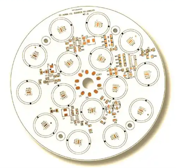
What is LED Surgical Shadowless Light Copper Core PCB?
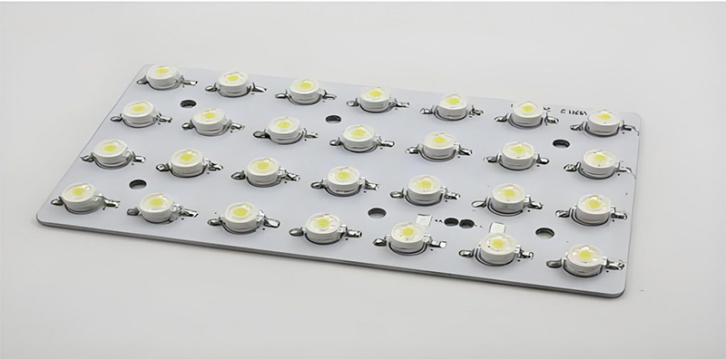
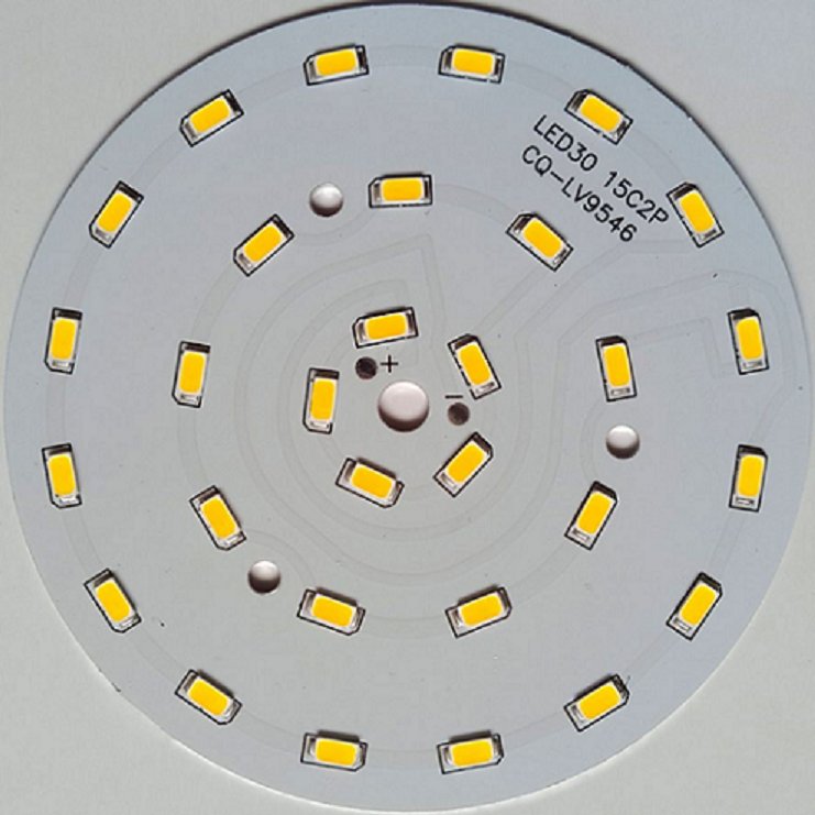
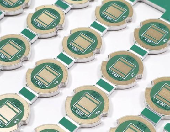
An LED Surgical Shadowless Light Copper Core PCB is a type of metal core printed circuit board specifically designed for high-power LED surgical lighting systems, where stable illumination and efficient heat dissipation are essential.
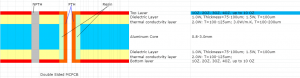
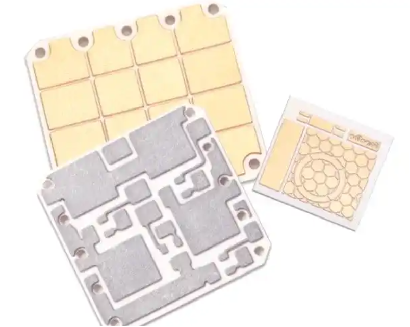
Core Structure
It typically consists of:
- A copper circuit layer for LED mounting
- A thermally conductive dielectric layer
- A solid copper core for heat transfer
Compared with standard PCBs, the copper core enables faster heat conduction away from LEDs, helping maintain consistent light output during long surgical procedures.
Therefore, this type of PCB serves as the thermal and structural foundation of surgical shadowless lighting systems.
What Makes LED Surgical Shadowless Light Copper Core PCB Essential for Heat Management?
The answer is straightforward. Copper core PCBs provide superior heat dissipation, reducing LED junction temperature and maintaining luminous efficiency during long surgeries.
Thermal Advantage Explained
- Copper thermal conductivity is 2x–3x higher than aluminum
- Rapid heat spreading reduces hot spots
- Improves LED lifespan by over 30%
Engineering Insight
Lower junction temperature leads to stable color rendering index (CRI), which is critical in surgical precision.
Therefore, copper core PCB is not optional but essential for high-end surgical lighting performance.
How Does Copper Core PCB Compare with Aluminum PCB in Surgical Lighting?
Direct comparison shows copper core PCBs outperform aluminum in thermal and reliability aspects.
Comparison Table
| Parameter | Copper Core PCB | Aluminum PCB |
|---|---|---|
| Thermal Conductivity | ~380 W/m·K | ~200 W/m·K |
| Heat Spreading | Excellent | Moderate |
| Mechanical Strength | High | Medium |
| LED Lifespan Impact | Longer | Shorter |
| Application Level | High-end medical | General lighting |
From an engineering perspective, copper core PCB ensures consistent performance in mission-critical environments like operating rooms.
Why Are Thermal Stability and Uniform Light Output Critical in Surgical Lighting?
Stable illumination ensures accurate tissue differentiation and reduces surgeon fatigue during long procedures.
Key Performance Requirements
- Uniform light distribution
- No flickering or color drift
- Long-term stability under continuous operation
Role of PCB
The PCB acts as a thermal and structural platform. Poor heat management leads to uneven brightness.
As a result, copper core PCB becomes the preferred solution for maintaining optical consistency.
How to Design LED Copper Core PCB for Surgical Shadowless Lights?
Designing an LED Copper Core PCB Surgical Shadowless Light is essentially a thermal-driven engineering task. The goal is not just to place LEDs on a board, but to ensure that heat generated by each LED can be transferred efficiently to the copper core and then dissipated uniformly across the entire lamp structure. If thermal design is weak, the result is immediate: brightness inconsistency, color drift, and reduced reliability.
Thermal design must start from junction temperature control
The most practical way to begin is to define the allowable LED junction temperature, because this directly determines light stability in surgical environments.
A simplified engineering model is:
Tj = Ta + P × Rθ(total)
Where:
- Tj = LED junction temperature
- Ta = ambient temperature inside the lamp head
- P = power per LED
- Rθ(total) = total thermal resistance from junction to ambient
This formula is not theoretical—it directly tells you whether your PCB structure is acceptable. If Rθ(total) is too high, no layout optimization can compensate later.
Use thermal budget to guide PCB stack-up design
Once the target temperature is defined, the next step is to allocate thermal resistance across each layer.
In a Copper Core PCB for LED Surgical Shadowless Light, the thermal path can be simplified into:
- LED package → solder layer
- dielectric layer → copper core
- interface material → lamp housing
Among these, the dielectric layer is usually the weakest link, because its thermal conductivity is much lower than copper.
A practical estimation method:
R = L / (k × A)
Where:
- L = thickness of dielectric
- k = thermal conductivity
- A = effective heat transfer area
This equation helps you answer a very practical question:
👉 Is my dielectric layer too thick for this LED power level?
If the calculated resistance is too high, you must:
- reduce dielectric thickness
- increase thermal pad area
- or switch to higher conductivity materials
Estimate LED heat generation correctly before layout
Before routing anything, you should estimate how much heat each LED generates.
Basic calculation:
P = Vf × If
For example:
- Forward voltage = 3.0 V
- Current = 700 mA
Then:
P = 3.0 × 0.7 = 2.1 W per LED
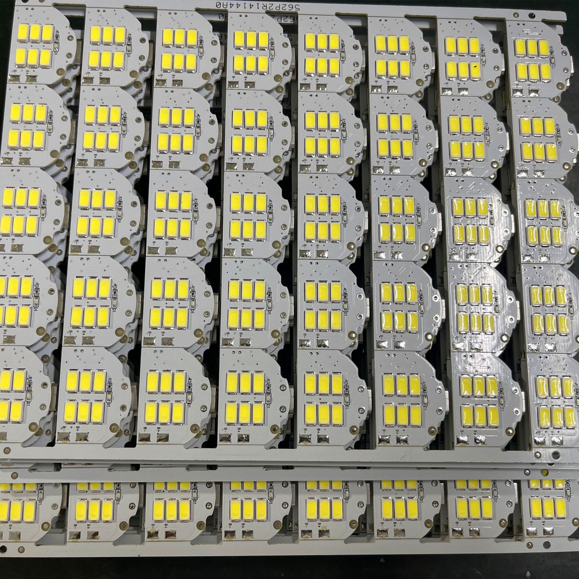
If your module contains 20–30 LEDs, the total heat load becomes significant. This is why surgical lighting PCBs behave more like thermal modules than traditional signal boards.
Why copper core PCB is structurally necessary, not optional
In this application, copper is not chosen for convenience—it is chosen because of heat spreading capability.
Compared with other structures:
- Copper distributes heat laterally much faster
- Reduces local hot spots under LED arrays
- Improves temperature uniformity across the entire light surface
This uniformity is especially important in shadowless lighting, where uneven temperature leads directly to uneven illumination.
Layout symmetry directly affects both optics and temperature
In surgical lighting, LED layout is not only about light distribution, but also about thermal balance.
A good layout should:
- distribute LEDs evenly across the board
- avoid thermal concentration in one region
- keep power density consistent
- maintain symmetrical current paths
If one side of the board carries more heat, that region will age faster and create brightness variation over time.
Maximize thermal conduction area in copper layer
The copper layer is your main heat spreader, so its usage must be intentional.
Key practices:
- Use large copper planes under LED pads
- Minimize unnecessary segmentation of copper areas
- Avoid narrow thermal bottlenecks
- Ensure direct thermal path to the copper core
Even small layout decisions, such as cutting copper for routing convenience, can increase thermal resistance significantly.
Flatness is a hidden but critical design parameter
Flatness is often ignored at the design stage, but it directly affects:
- LED solder joint quality
- thermal interface contact
- optical alignment
If the PCB warps after reflow, part of the LED array may lose proper contact with the heat sink. That creates localized overheating even if your thermal calculation was correct.
So design must consider:
- balanced copper distribution
- proper stack-up symmetry
- controlled material expansion
DFM considerations must be integrated early
Design for manufacturability is not a separate step—it must be built into the design phase.
Important factors include:
- compatibility with reflow profile
- solder paste thickness control
- heavy copper handling capability
- panelization strategy
Ignoring DFM often leads to:
- low assembly yield
- inconsistent solder joints
- thermal performance variation between batches
Engineering validation is the final step
After design, validation is essential.
A practical method:
- measure solder point temperature (Ts)
- calculate junction temperature using thermal resistance
- compare with design target
This closes the loop between design and real-world performance.
In practice, designing an LED Copper Core PCB Surgical Shadowless Light is a balance between thermal calculation, layout symmetry, material selection, and manufacturability. A well-designed structure ensures stable light output, uniform temperature distribution, and long-term reliability, which are all critical in surgical environments.
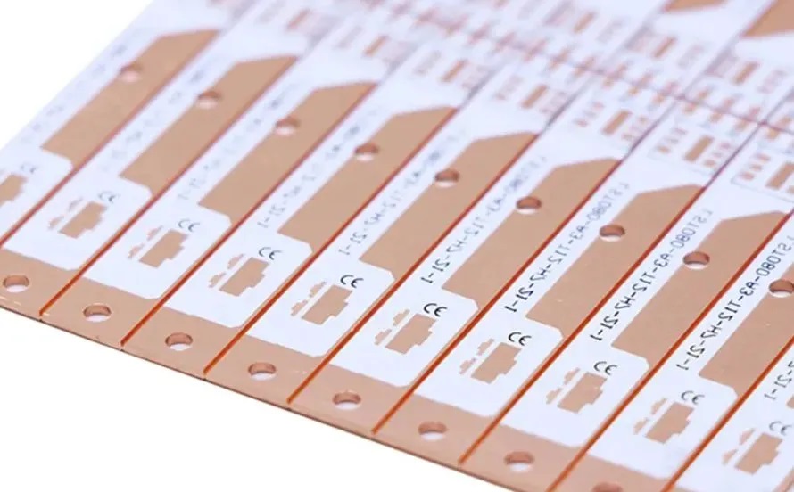
What Are the Common Challenges in LED Surgical Shadowless Light PCB Manufacturing?
Users often struggle with thermal mismatch, warpage, and inconsistent soldering quality.
Typical Challenges
- CTE mismatch causing stress
- Uneven solder joints due to heavy copper
- Surface flatness affecting LED alignment
- Thermal cycling reliability issues
Our Solutions
- Controlled lamination process
- Precision surface finishing
- Optimized reflow profile
- Full AOI and X-ray inspection
Overall, solving these issues requires both material expertise and process control capability.
How Do We Solve Real User Pain Points in Surgical Lighting PCB Projects?
Users demand reliability, fast delivery, and consistent quality across batches.
Pain Points
- Inconsistent brightness across batches
- Thermal failure after long operation
- Long development cycles
- Assembly defects in high-power LEDs
Our Approach
- Thermal simulation before production
- DFM feedback within 24 hours
- Automated SMT + selective soldering
- Burn-in testing for reliability validation
Notably, addressing these challenges early significantly improves product stability and time-to-market.
What Certifications Ensure Quality in LED Surgical Shadowless Light Copper Core PCB?
Certifications validate process control and product reliability in medical-grade applications.
| Certification | Scope |
|---|---|
| ISO 9001 | Quality Management |
| ISO 13485 | Medical Device Manufacturing |
| IATF 16949 | Automotive Quality Standard |
| AS9100D | Aerospace Quality System |
| RoHS | Environmental Compliance |
This means certified processes ensure consistent performance in critical medical lighting systems.
Which Industries Use LED Surgical Shadowless Light Copper Core PCB Most?
These PCBs are widely used in high-reliability lighting systems.
Top Applications
- Medical surgical lighting systems
- Dental operating lamps
- High-end diagnostic equipment
- Precision industrial inspection lighting
Case Example
A surgical lighting system using copper core PCB achieved 25% longer LED lifespan and improved light uniformity.
In short, these PCBs are critical in environments where lighting accuracy directly impacts outcomes. EBest Circuit (Best Technology) is a specialized manufacturer of LED Surgical Shadowless Light Copper Core PCB, with deep expertise in high-thermal medical lighting applications. We understand the strict requirements of surgical environments, including sterilization compatibility, stable heat dissipation, and long-term reliability, and we integrate these standards directly into our material selection and process control.
Our engineering-driven approach ensures optimized thermal structures, uniform temperature distribution, and consistent optical performance, helping lighting systems maintain high brightness without shadow or drift. With certified manufacturing systems, fast response DFM support, and stable delivery capability, we provide a reliable solution for projects that demand both medical compliance and engineering precision. Pls feel free to call us anytime at +86-755-2909-1601 to discuss your LED Surgical Shadowless Light Copper Core PCB project.
How Does Surface Finish Impact LED Performance in Copper Core PCB?
Surface finish affects solderability, thermal interface, and long-term reliability.
Common Finishes
- ENIG – stable and widely used
- ENEPIG – superior for high-reliability applications
Engineering Impact
Better surface finish ensures consistent solder joints and improved thermal conduction.
To sum up, selecting the right surface finish enhances both manufacturing yield and product lifespan.
Why Use LED Surgical Shadowless Light Copper Core PCB in High-End Medical Equipment?
Beyond surgical lights, the Surgical Shadowless Light LED Copper Core PCB is essential for any equipment where heat is the enemy of accuracy. High-intensity light sources generate localized heat that can warp thin boards; however, the rigidity of a Copper Core PCB LED Surgical Shadowless Light maintains a perfectly flat focal plane.
Industry Applications:
- Endoscopy Light Sources: Requires compact, high-power LED Copper Core PCB Surgical Shadowless Light modules.
- Dental Operatory Lights: Benefits from the long-term reliability of Copper Core PCB for LED Surgical Shadowless Light.
- Diagnostic Imaging: Uses LED Surgical Shadowless Light Copper Core PCB tech for high-output X-ray collimators.
- Veterinary Surgery: Provides durable LED Surgical Shadowless Light with Copper Core PCB solutions for rugged use.
Therefore, investing in copper-core technology is a strategic move to future-proof any high-intensity medical lighting product line.
Why Is Flatness Control Critical in Surgical Lighting PCB Assembly?
Flatness directly affects LED alignment and optical performance.
Key Factors
- Warping leads to uneven light output
- Affects optical lens positioning
- Impacts assembly accuracy
Control Methods
- Precision lamination
- Controlled cooling process
- Post-process flattening
From a manufacturing standpoint, flatness control is essential for achieving consistent lighting performance.
To sum up, LED surgical shadowless light copper core PCB is a high-thermal-conductivity circuit board designed to support high-power LEDs in medical lighting systems. It ensures efficient heat dissipation and stable illumination. EBest Circuit (Best Technology) provides LED Surgical Shadowless Light Copper Core PCB with high reliability, stable delivery, and full-process support. If you are looking for a trusted manufacturing partner, pls feel free to contact us at sales@bestpcbs.com to start your project at any time.
FAQs About LED Surgical Shadowless Light Copper Core PCB
What is the thermal conductivity of a copper core PCB LED surgical shadowless light?
Our LED Surgical Shadowless Light Copper Core PCB typically features a thermal conductivity of 380W/m.K to 400W/m.K for the copper base, with dielectric layers ranging from 3W/m.K to 12W/m.K depending on your specific insulation needs.
How to choose the right thickness for a surgical shadowless light LED copper core PCB?
Choosing the right thickness for a Surgical Shadowless Light LED Copper Core PCB depends on the weight constraints of the lamp head and the heat load; common thicknesses range from 1.0mm to 3.0mm, with 1.6mm being the industry standard for LED Copper Core PCB Surgical Shadowless Light applications.
Why use copper core PCB for surgical lighting?
Copper core PCBs provide superior heat management, reducing LED degradation and ensuring consistent light output during long surgical procedures.
How does copper core PCB improve LED lifespan?
By lowering junction temperature, copper core PCBs reduce thermal stress, extending LED lifespan significantly.
What surface finish is best for medical LED PCB?
ENEPIG is preferred for high-reliability applications due to its superior corrosion resistance and bonding performance.
Can copper core PCB be used in other industries?
Yes, it is widely used in automotive lighting, industrial systems, and high-power LED applications.
Finally, addressing these technical questions early in the design phase ensures a smoother transition from prototype to mass production for your medical lighting products.