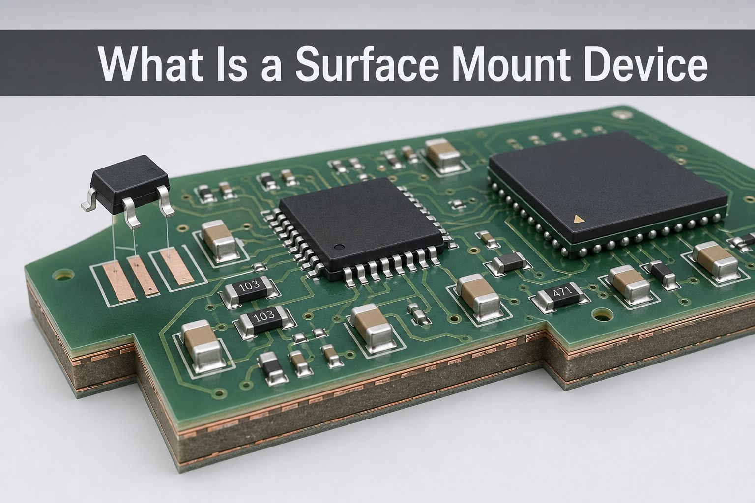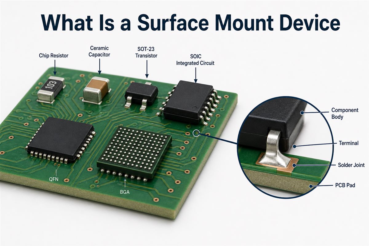
A surface mount device (SMD) is an electronic component designed to be soldered directly onto pads on the surface of a printed circuit board. Unlike a through-hole part, it normally does not need long leads inserted through drilled holes. This mounting method supports compact products, dense circuit layouts, short electrical paths, and automated assembly.
This guide answers what is a surface mount device in practical terms. It also organizes common surface mount device components, explains the main types of SMD packages, and follows those parts through the surface mount technology process. The goal is to help designers, buyers, and production teams use the same language when reviewing a BOM, PCB layout, quotation, or assembly plan.
What Does Surface Mounted Device Mean in Electronics?
In electronics, a surface mounted device means a component whose terminals are joined to conductive pads on the outer surface of a PCB. The terminals may be metal end caps, gull-wing leads, J-leads, flat bottom contacts, an exposed thermal pad, or an array of solder balls. The package style changes, but the defining feature is the same: the component is attached to surface pads rather than installed primarily through lead holes.
The related terms are easy to confuse:
- SMD is the physical component.
- SMT, or surface mount technology, is the method used to place and solder SMDs.
- SMA may refer to a surface mount assembly.
- PCBA is the completed printed circuit board assembly after components have been installed.
So, when someone asks “what is SMD in electronics?”, the short answer is: it is the part, not the whole manufacturing process. A chip resistor is an SMD; stencil printing, pick-and-place, and reflow soldering are stages of SMT.
Surface Mount Device Components: A Practical SMD Components List
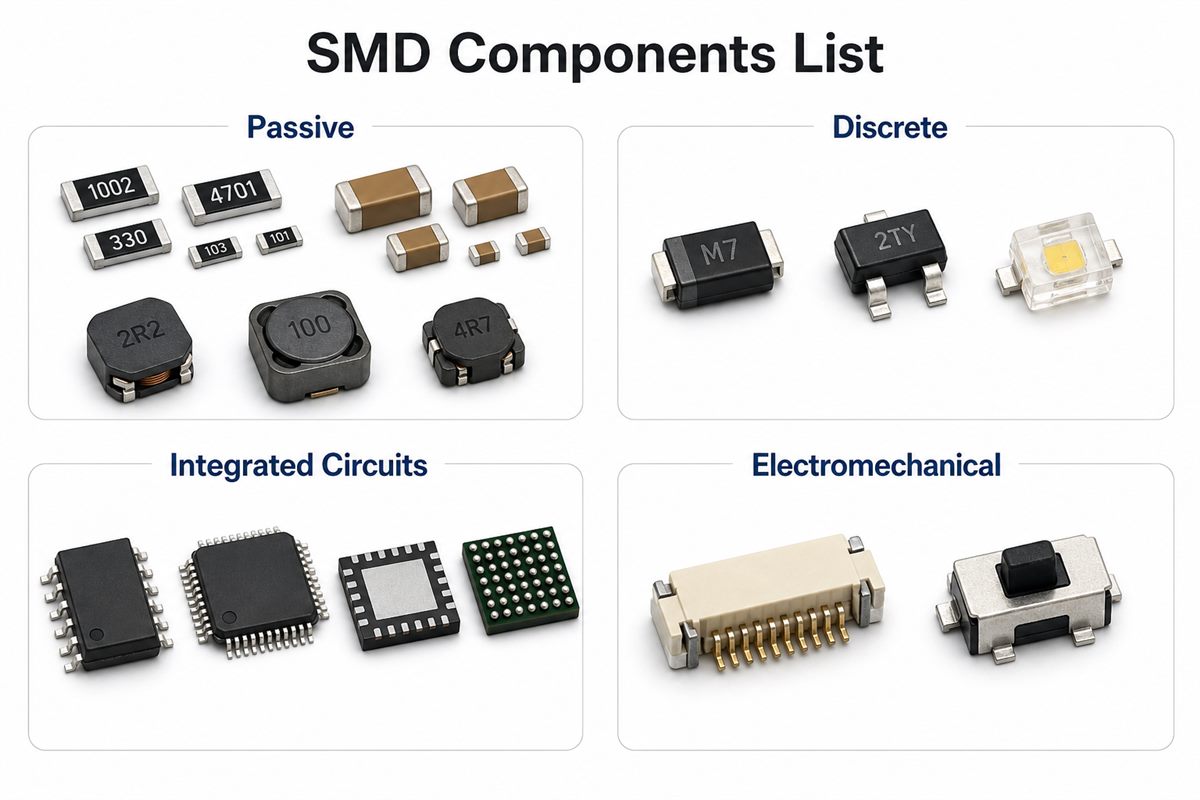
Surface mount device components include passive parts, discrete semiconductors, integrated circuits, optoelectronic parts, and some electromechanical devices. Grouping them by function is more useful than treating every package code as a separate component category.
| Category | Common examples | Typical circuit role |
|---|---|---|
| Passive | Resistors, capacitors, inductors, ferrite beads | Biasing, filtering, decoupling, energy storage and EMI control |
| Discrete semiconductor | Diodes, transistors, MOSFETs, TVS devices | Switching, amplification, rectification and protection |
| Integrated circuit | Op-amps, regulators, drivers, memory and microcontrollers | Analog, power, logic, control and data processing |
| Optoelectronic | LEDs, photodiodes and optocouplers | Indication, sensing and isolation |
| Electromechanical | Connectors, switches, buzzers and relays | Physical connection, user input and mechanical switching |
A useful SMD components list must include more than part names. For production, each BOM item should also identify the manufacturer part number, value, tolerance, voltage or power rating, package, approved substitute policy, quantity, and reference designators. Those fields connect the electrical design to sourcing, footprint verification, feeder setup, and inspection.
Types of SMD and Common Package Families
The main types of SMD can be classified by function, terminal structure, or package family. Package classification is especially important because it affects PCB land patterns, placement accuracy, solder-joint visibility, thermal behavior, inspection, and rework.
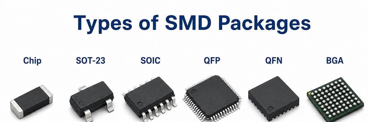
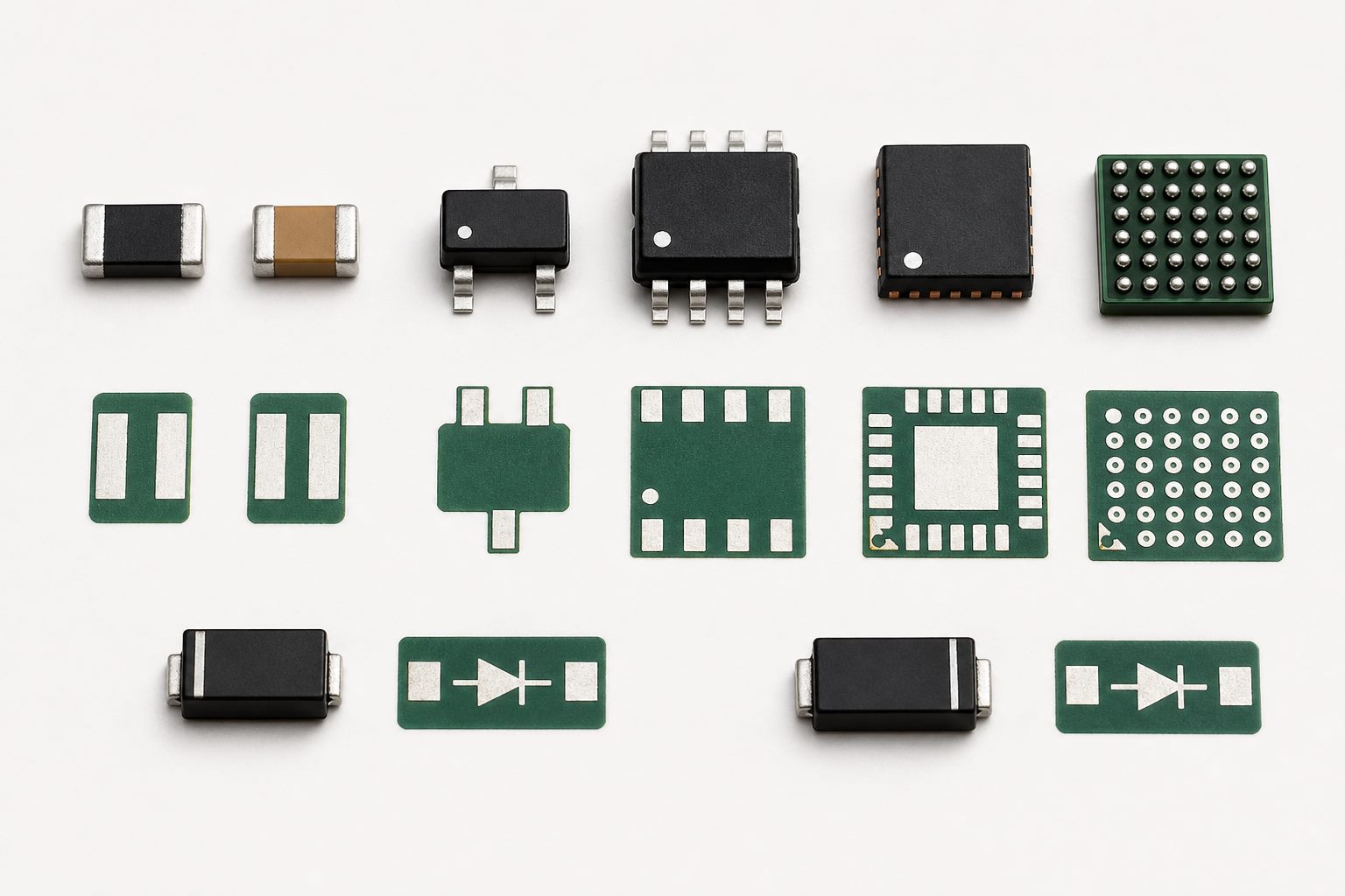
- Chip packages: rectangular resistors, capacitors, inductors, and ferrite beads with metalized end terminals. Common size codes include 0402, 0603, 0805, and 1206 in the imperial system.
- SOT packages: small transistor and diode outlines such as SOT-23, often used for discrete semiconductors and compact regulators.
- SOIC and TSSOP: integrated circuits with visible leads on two sides. They are comparatively easy to inspect and rework.
- QFP: IC packages with gull-wing leads on four sides. Fine-pitch versions need accurate printing, placement, and soldering.
- QFN and DFN: leadless packages with bottom contacts, often with an exposed center pad for thermal and electrical performance.
- BGA: high-I/O packages that connect through an array of solder balls under the body. Their hidden joints typically require X-ray inspection when joint-level evidence is needed.
Package names alone are not enough to create a footprint. Two parts described as QFN may have different body sizes, pitches, pad dimensions, or exposed-pad requirements. The component datasheet and approved land-pattern data should control the design.
What Is a Surface-Mount Device (SMD) Package?
A surface-mount device (SMD) package is the physical enclosure and terminal arrangement that allows the electronic die or functional element to connect to a PCB. It defines dimensions, terminal locations, pitch, polarity or pin-one indicators, thermal paths, and the interface used by assembly equipment.
The package, PCB footprint, and component value are separate facts. For example, several resistor values may share the same 0603 package, while one IC function may be offered in SOIC, QFN, and BGA options. Choosing the right package requires balancing board area, electrical performance, heat dissipation, sourcing availability, assembly capability, inspection access, and rework needs.
Do not assume a size code means the same physical dimensions in every naming system. Chip components are commonly described with imperial and metric codes, so the design team should state the convention and verify actual dimensions in the datasheet. This avoids selecting a correct electrical value in the wrong physical package.
What Is the Surface Mount Technology Process?
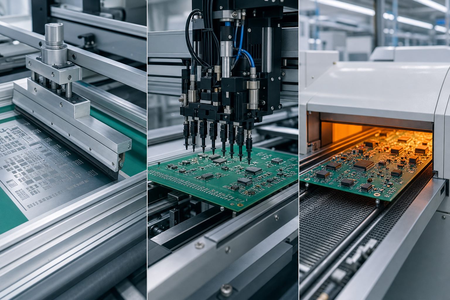
The surface mount technology process normally applies solder paste to PCB pads, verifies the paste deposit, places SMDs, reflows the solder, and inspects the assembled board. Programming, electrical testing, cleaning, conformal coating, depaneling, or final assembly may follow depending on the product.
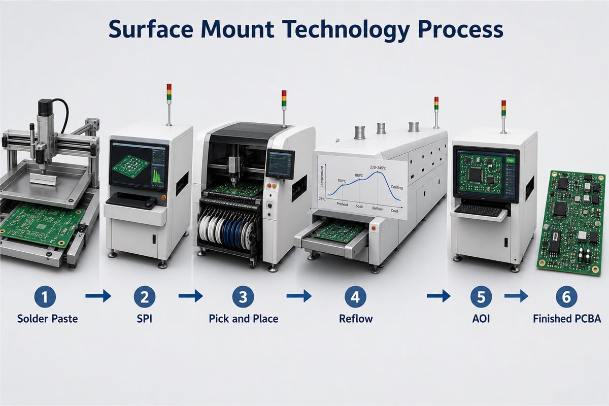
- Solder paste printing: a stencil transfers controlled deposits of solder paste onto the PCB pads. Aperture design, stencil thickness, paste condition, and printing alignment influence deposit quality.
- Solder paste inspection (SPI): the system measures paste position, area, height, and volume so printing problems can be corrected before components are added.
- Pick and place: a surface mount machine collects components from reels, trays, or tubes, identifies them, and places them at programmed coordinates and orientations.
- Reflow soldering: the assembly passes through controlled heating zones. The paste activates, melts, wets the pads and terminals, then solidifies during cooling.
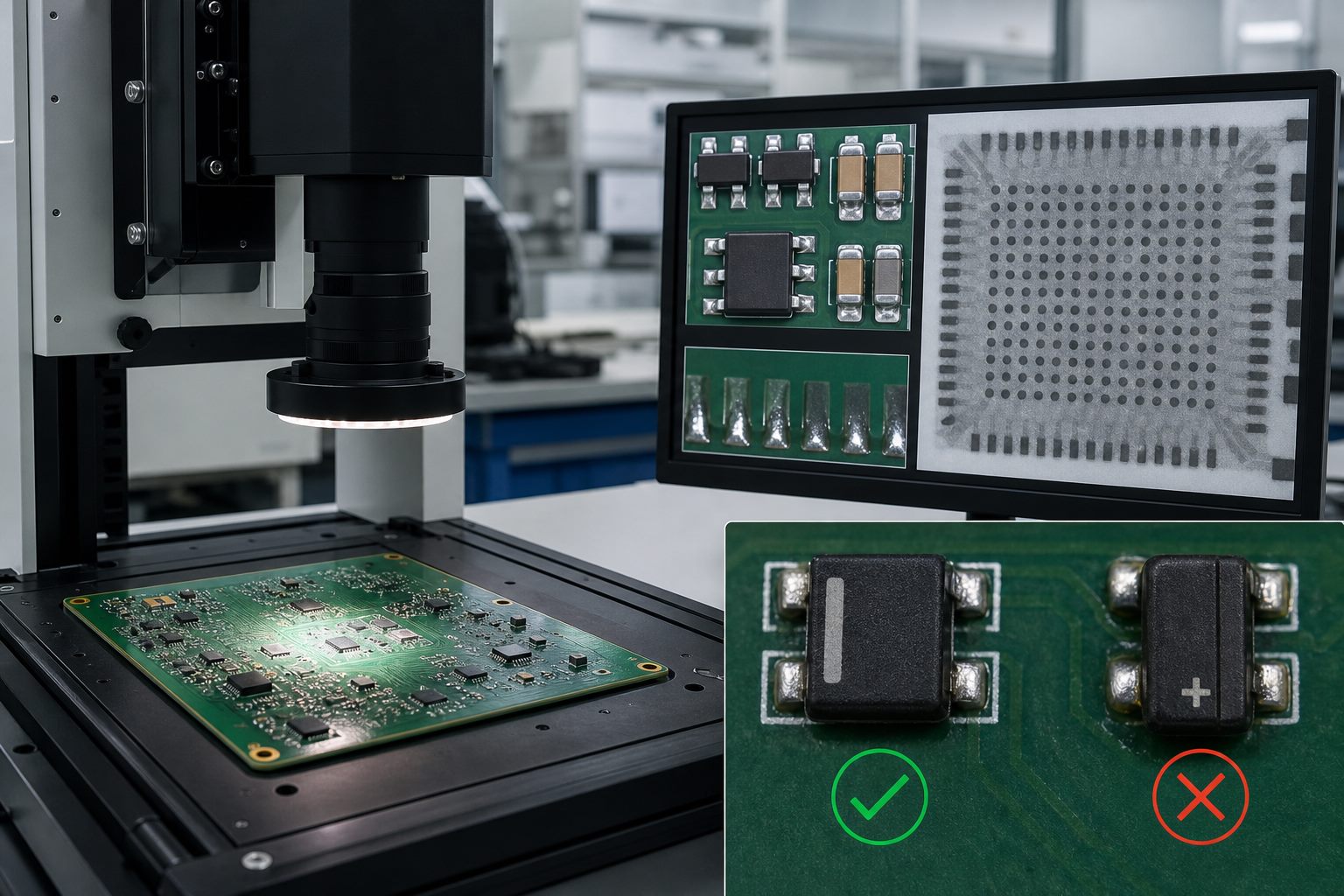
- Inspection: automated optical inspection checks visible placement and solder conditions. X-ray can examine hidden BGA or bottom-terminated joints, while electrical and functional tests verify circuit behavior.
The assembly result depends on the full system rather than one machine. PCB pad design, the SMT stencil, solder paste, component packaging, placement data, reflow profile, and inspection criteria must work together. Teams preparing a build can use a professional PCB assembly service to review these inputs before production.
How Do SMDs Compare with Through-Hole Components?
SMDs are usually preferred when compact size, short interconnections, high component density, and automated placement matter. Through-hole components remain useful when leads must provide stronger mechanical anchoring, when a specific high-power or high-voltage part is only available in a leaded package, or when manual handling and field replacement are priorities.
| Design factor | SMD | Through-hole |
|---|---|---|
| Mounting | Soldered to surface pads | Leads pass through drilled holes |
| Board density | Supports small parts and dense layouts | Consumes hole and routing area |
| Automation | Well suited to high-speed placement and reflow | May require insertion and wave or selective soldering |
| Mechanical anchoring | Depends on pads, solder joints, and package design | Leads through the board can provide extra retention |
| Inspection | Some bottom joints are hidden | Many joints are visually accessible on the opposite side |
Many products use mixed technology. A board may use hundreds of SMDs for signal and control functions while retaining through-hole connectors, transformers, or large capacitors where mechanical or electrical requirements justify them. For a terminology-focused comparison, see SMT vs SMD.
How Should You Select Surface Mount Device Components?
Select surface mount device components by checking electrical ratings first, then confirming package and manufacturing compatibility. A smaller package is not automatically better; it may reduce routing space while increasing placement, inspection, thermal, sourcing, or rework difficulty.
- Confirm value, tolerance, voltage, current, power, frequency, and temperature requirements.
- Match the exact package and terminal pattern to the verified PCB footprint.
- Check polarity, pin-one, diode cathode, LED orientation, and connector mating direction.
- Review component height, courtyard, nozzle access, and spacing around test points or mechanical features.
- Check moisture sensitivity, storage, baking, and reflow limits for sensitive packages.
- Consider thermal pads, copper spreading, vias, airflow, and enclosure temperature for power devices.
- Verify availability, lifecycle status, minimum order conditions, and approved alternatives.
- Ensure the assembler can print, place, inspect, and rework the chosen pitch and package.
Before release, compare the BOM package field with the CAD footprint name and the manufacturer datasheet. This three-way check catches common mismatches such as metric-versus-imperial chip sizes, similar package names with different pitches, or an exposed pad missing from the PCB land pattern.
Which SMD Assembly Defects Matter Most?
The most important SMD assembly defects include insufficient solder, solder bridges, opens, tombstoning, component shift, reversed polarity, lifted leads, voiding, and hidden-joint problems. Their causes may come from pad geometry, stencil design, paste deposition, placement, component condition, thermal profile, or handling.
- Tombstoning: one end of a small chip component lifts during reflow, often because wetting forces or heating are unbalanced.
- Solder bridges: unintended solder connects adjacent terminals, potentially causing an electrical short.
- Opens: a terminal does not form a reliable electrical connection because of insufficient paste, poor wetting, warpage, or misalignment.
- Polarity errors: a diode, LED, electrolytic capacitor, or IC is placed in the wrong orientation.
- Hidden-joint defects: BGA, QFN, and other bottom-terminated packages may require X-ray, electrical test, or process evidence because optical inspection cannot see every joint.
Quality control should connect each defect to a prevention and detection method. SPI controls paste deposition, placement verification controls orientation and position, the reflow profile controls soldering conditions, AOI checks visible features, and X-ray or electrical tests address hidden or functional risks.
Frequently Asked Questions About Surface Mount Devices
1. What does surface mount mean?
Surface mount means attaching an electronic component directly to conductive pads on the surface of a PCB instead of primarily inserting its leads through holes.
2. What is SMD in electronics?
SMD stands for surface mount device. It is a component package designed for direct surface mounting, such as a chip resistor, SOT-23 transistor, QFN IC, or BGA.
3. Is SMD the same as SMT?
No. SMD is the component, while SMT is the manufacturing method used to place and solder surface mount components.
4. What is a surface mount machine?
A surface mount machine usually means a pick-and-place system that takes components from feeders or trays and places them on solder-pasted PCB pads according to programmed coordinates.
5. What is a surface mount device LED?
An SMD LED is a light-emitting diode packaged for surface mounting. Its footprint, polarity marks, optical output, color, current rating, and thermal needs must match the design.
6. Are all surface mount components polarized?
No. Many resistors and ceramic capacitors are non-polarized. Diodes, LEDs, electrolytic capacitors, transistors, and ICs normally require a defined orientation.
7. Why do some SMDs have no readable marking?
Very small packages may not have enough printable area. Identification should come from the BOM, manufacturer part number, reel label, feeder record, and controlled material traceability rather than appearance alone.
8. What do 0402, 0603, and 0805 mean?
They are common chip-package size codes. Because imperial and metric codes can be confused, always confirm the stated convention and actual body dimensions in the datasheet.
9. Can surface mount devices be soldered by hand?
Many larger chip, SOIC, and SOT packages can be hand-soldered with suitable tools and skill. Fine-pitch, QFN, BGA, and very small chips generally need more controlled equipment and inspection.
10. Can SMDs be mounted on both sides of a PCB?
Yes. Double-sided SMT is common, but the process sequence, component mass, adhesive needs, reflow exposure, and handling plan must be reviewed.
11. How are surface mount devices tested?
Testing may include AOI, X-ray, in-circuit testing, flying-probe testing, programming, boundary scan, functional testing, and product-specific verification. The right combination depends on package visibility and circuit risk.
12. What files are needed for SMD assembly?
A controlled package commonly includes Gerber or ODB++ data, drill files, BOM, centroid or pick-and-place data, assembly drawings, polarity notes, approved substitutions, test requirements, and any special process instructions.
Summary
A surface mount device is a component designed to connect directly to pads on a PCB surface. Surface mount device components range from simple chip resistors to fine-pitch ICs and BGAs, while the surface mount technology process turns those parts into an assembled board through printing, placement, reflow, and inspection.
For a reliable build, treat the electrical part number, SMD package, PCB footprint, polarity data, BOM, placement file, stencil, and inspection plan as one connected system. This practical definition of surface mount device components helps prevent package mismatches and improves communication from design through production.
Need support with an SMD assembly project? Share your PCB data, BOM, placement files, and quality requirements with Best Technology for an engineering review and quotation.