When people search for what is a good SNR for WiFi, they usually want a clear number. Is 15 dB enough? Is 20 dB good? Is 30 dB ideal? In simple terms, WiFi works better when the useful signal is much stronger than the surrounding noise. That is why signal bars alone are not enough. A device may show strong signal strength, but if the noise floor is high, the real connection can still be slow, unstable, or easy to drop.
For wireless products, WiFi SNR is also related to how the device is built. PCB layout, RF trace routing, grounding, antenna keep-out handling, controlled impedance, power noise control, SMT assembly, RF connector soldering, and shield-can assembly can all affect final performance. This article explains WiFi SNR in a practical way and focuses on what a PCB and PCBA manufacturer can support. If you are developing a WiFi PCB or PCBA project, you are welcome to send your files and requirements to sales@bestpcbs.com for a careful review.

What Does SNR Stand for in WiFi?
SNR stands for signal-to-noise ratio. In WiFi, it shows the difference between the useful wireless signal and the surrounding noise. It is usually measured in decibels, written as dB.
A simple way to understand it is:
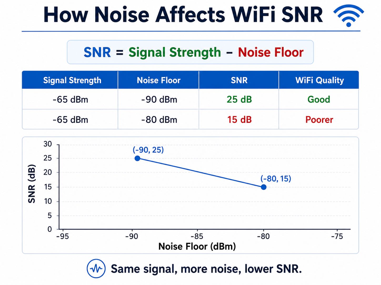
SNR = Signal Strength – Noise Floor
SNR is not the same as signal strength. Full signal bars do not always mean a high SNR.
For example:
| Signal Strength | Noise Floor | SNR | WiFi Quality |
|---|---|---|---|
| -65 dBm | -90 dBm | 25 dB | Good |
| -65 dBm | -80 dBm | 15 dB | Weaker |
In both cases, the WiFi signal strength is the same: -65 dBm. The real difference is the noise floor. When the surrounding noise rises from -90 dBm to -80 dBm, the SNR drops from 25 dB to 15 dB.
This is why a device can be close to the router but still have a poor WiFi experience. Nearby WiFi networks, Bluetooth devices, microwave ovens, switching power supplies, motors, displays, and other noise sources can raise the noise floor. When that happens, RSSI or signal bars may still look good, but the actual connection can become slow or unstable.
So, when evaluating WiFi quality, do not only look at RSSI or signal bars. SNR gives a clearer view of how clean the WiFi signal is compared with the surrounding noise.
For wireless products, this matters because the end user does not care whether the problem comes from the router, enclosure, PCB layout, power noise, antenna position, or PCBA process. They only notice unstable connection, slower response, packet loss, or shorter range.
What Is a Good SNR for WiFi?
A good SNR for WiFi is usually around 20 dB or higher for normal data communication. For better stability, 25–30 dB is a stronger target range. If the SNR is above 30 dB, the WiFi connection usually has a comfortable margin over noise.
In practical terms:
| SNR Rating | General Meaning |
|---|---|
| Below 10 dB | Poor |
| 10–15 dB | Weak |
| 15–20 dB | Fair |
| 20–25 dB | Good |
| 25–30 dB | Very good |
| 30 dB+ | Excellent |
So, what is a good signal to noise ratio for WiFi? For many wireless products, 20 dB or higher is a useful baseline. For products that need better reliability, such as WiFi cameras, IoT gateways, smart control devices, medical monitoring products, and industrial terminals, a higher SNR is preferred.
However, there is no single ideal SNR for every product. A battery-powered sensor, a smart plug, a WiFi camera, and an industrial gateway do not have the same communication load or installation environment.
A simple sensor may only send small data packets. A WiFi camera needs more stable bandwidth. An industrial gateway may need reliable communication in a noisy electrical environment. That is why the ideal SNR depends on the product application, wireless module, antenna type, enclosure, power system, and final test environment.
For PCB and PCBA projects, the target should come from the customer’s product requirement, wireless module datasheet, RF test plan, and application environment. The PCB layout and manufacturing team can then support the project by following the approved stack-up, impedance requirement, grounding rule, antenna keep-out rule, and assembly instruction.
What Do Different SNR Values Mean for WiFi Quality?
Different SNR values show how much margin the WiFi signal has over the surrounding noise. The higher the SNR, the easier it is for the receiver to separate useful data from unwanted interference.
| WiFi SNR | Quality Level | Practical Meaning |
|---|---|---|
| 0–10 dB | Poor | Unstable connection |
| 10–15 dB | Weak | Basic connection only |
| 15–20 dB | Fair | Usable, but limited margin |
| 20–25 dB | Good | Suitable for normal WiFi use |
| 25–30 dB | Very Good | Better stability and speed |
| 30 dB+ | Excellent | Strong signal margin |
For example, SNR 15 may still support basic WiFi communication, but it is not ideal for stable data transmission. It may work in a clean environment, but the margin is limited. If the noise increases, the device moves farther from the router, or the enclosure weakens the antenna performance, the connection may become unstable.
SNR 6 is usually too low. At this level, the useful signal is very close to the noise floor. The device may still connect, but slow speed, packet loss, retransmission, or disconnection can occur.
A high SNR is usually better because the receiver has a cleaner difference between the useful signal and the noise. A high signal-to-noise ratio does not solve every WiFi issue, but it gives the system more room to work.
For wireless product development, the goal is not only to reach a good value in a perfect lab condition. The product should also maintain enough margin after enclosure assembly, component tolerance, PCB production, SMT assembly, and real-world operation.
Why Can WiFi Signal Strength Be Good but SNR Still Poor?
A common misunderstanding is that strong WiFi signal means good WiFi quality. This is not always true. If the signal is strong but the noise is also high, the SNR will still be low.
In other words, a device can show full signal bars but still suffer from slow speed, retransmission, packet loss, or unstable connection.
This happens because WiFi quality depends on both sides of the equation:
- Signal strength shows how strong the useful WiFi signal is.
- Noise floor shows how much unwanted background noise exists.
- SNR shows the gap between them.
If the signal is strong and the noise is low, the SNR is good. If the signal is strong but the noise is also high, the SNR becomes worse.
In real products, noise can come from many places:
- Neighboring WiFi networks
- Bluetooth devices
- Microwave ovens
- Switching power supplies
- DC-DC converters
- High-speed digital circuits
- Motors, relays, and power drivers
- Displays, cameras, USB circuits, and other modules
- Poor grounding or noisy return paths
- Bad RF connector contact or weak soldering
Some of these issues are outside the PCB factory’s control. For example, the factory cannot control the customer’s router, building structure, wireless channel, firmware, or final installation environment.
But some issues are related to hardware execution. If noisy circuits are placed too close to the WiFi section, if the RF trace has poor reference grounding, if the antenna area is blocked by copper or metal, or if the RF connector is not soldered well, the wireless module may not perform as expected.
That is why WiFi SNR should not be treated only as a router setting. In embedded wireless devices, PCB layout and PCBA quality can affect whether the wireless module works close to its intended performance.
Which PCB Layout Factors Can Influence WiFi SNR?
PCB layout cannot decide the final WiFi SNR alone. The wireless chip, antenna, firmware, enclosure, access point, distance, and environment also matter. However, poor layout can reduce the performance margin of a WiFi device.
In WiFi PCB layout, the following points need careful control:
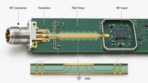
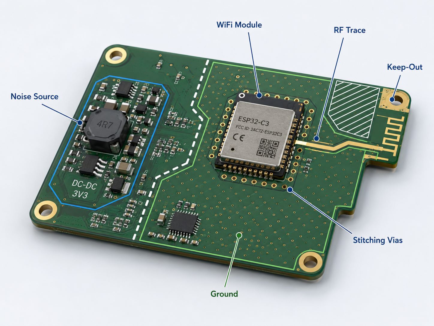
- RF trace path
The RF trace should be short, clean, and routed according to the WiFi module datasheet or customer-provided layout guide. If a 50Ω RF path is required, the trace geometry should match the approved stack-up. - Ground reference
RF traces need a stable reference plane. Broken ground, unnecessary slots, or poor ground continuity can disturb the return path and increase noise sensitivity. - Noise source placement
DC-DC converters, high-speed signals, motors, relays, displays, and large current loops should be kept away from RF-sensitive areas when the layout allows. - Antenna area
The antenna keep-out area should remain clear according to the module or antenna layout guide. Copper, ground, components, and metal structures should not be added into this area unless approved. - Via and shielding support
Ground stitching vias and shield-can grounding should follow the customer’s layout requirements. These details help create a cleaner local ground environment around RF sections.
A PCB layout team should not replace RF system design. Its practical role is to execute the layout correctly based on the customer’s schematic, datasheet, stack-up, impedance requirement, antenna guide, and mechanical constraints.
For PCB manufacturing, the production side should also protect the layout intent. Line width, copper thickness, dielectric thickness, registration, solder mask opening, via quality, and surface finish can all affect high-frequency reliability when the design is compact or impedance-sensitive.
Why Does Controlled Impedance Matter in WiFi PCB Layout?
Controlled impedance matters because WiFi RF traces work at high frequencies. At 2.4 GHz, 5 GHz, or 6 GHz, the RF path cannot be treated like an ordinary low-speed signal trace.
Many WiFi modules require a 50Ω single-ended RF trace between the module and the antenna connector, chip antenna, or external antenna path. To achieve this, the PCB layout and PCB fabrication process must work together.
Key factors include:
- PCB stack-up
- Dielectric thickness
- Copper thickness
- Trace width
- Reference ground plane
- Solder mask influence
- Impedance tolerance
- Test coupon requirement
For PCB manufacturing, controlled impedance is not only a drawing requirement. It must be supported by real production control. If the stack-up changes, the RF trace impedance may also change. If trace width, copper plating, or dielectric thickness are not stable, the final RF performance can shift.
This is where a PCB factory can provide practical value. The factory can review the stack-up, calculate impedance based on actual materials, control etching and lamination, and provide impedance testing when required.
For WiFi PCB projects, the customer should provide clear impedance requirements. If the project uses a WiFi module, the module datasheet or layout guide may already define the RF trace structure. The PCB layout should follow those requirements instead of guessing.
For PCBA projects, controlled impedance is only one part of the whole path. The assembly team should also protect the RF-related areas during SMT, reflow, cleaning, inspection, and handling. RF connectors, WiFi modules, antenna connectors, and shield cans should be assembled with consistent quality.
How Should Antenna Keep-Out Areas Be Handled in PCB Layout?
Antenna keep-out is one of the most important layout details in wireless products. It is also an area where the service boundary must be clear.
A PCB layout team can help implement antenna keep-out rules. But antenna design and RF tuning should be handled by the customer’s RF engineer, module supplier, or antenna specialist.
Many WiFi and Bluetooth modules provide layout instructions for antenna position and keep-out areas. These instructions may define board edge distance, copper clearance, ground clearance, component restriction, and nearby metal limitations.
In PCB layout execution, antenna keep-out usually means:
- No copper in the defined keep-out area
- No components inside the antenna clearance zone
- No high-speed traces crossing the antenna area
- No ground pour where the module guide forbids it
- No shield can or metal part over the antenna area unless approved
- Proper distance from batteries, displays, heat sinks, speakers, and metal enclosure parts
The most common mistake is treating the antenna area like normal empty PCB space. It is not. The antenna area is part of the wireless performance structure.
For PCB and PCBA production, the factory should check that the Gerber files follow the keep-out requirements. During assembly, the production team should also avoid adding labels, metal parts, tall components, or unexpected shielding structures that conflict with the antenna zone.
If the customer uses a certified WiFi module, following the module manufacturer’s layout guide is especially important. Poor placement can reduce range, change radiation behavior, or make the final product fail RF validation.
This does not mean the PCB factory is designing the antenna. It means the factory helps preserve the antenna conditions required by the customer’s approved design.
How Does PCB Grounding Affect WiFi Noise?
PCB grounding affects WiFi noise because RF signals need a clear return path. A clean ground reference helps the RF path behave more predictably. A broken or noisy ground structure can increase coupling, radiation, and signal instability.
In WiFi PCB layout, grounding should focus on these points:
- Continuous reference plane
RF traces should have a solid ground reference. Avoid routing RF traces over ground gaps, plane splits, or large voids. - Short return path
The return current should have a nearby path. A long or interrupted return path can create extra noise and unwanted radiation. - Ground stitching vias
Proper via stitching around RF sections, board edges, or shield-can areas can help improve local grounding. - Power noise isolation
Switching power circuits should be arranged carefully. Poorly placed DC-DC converters or noisy current loops may affect WiFi module stability. - Shield-can grounding
If a shield can is used, its grounding pads should be well connected and properly soldered during PCBA production.
Grounding cannot solve every WiFi problem, but it can reduce avoidable layout-related noise. For wireless products, clean grounding is one of the most important details in PCB layout execution.
Grounding quality also depends on manufacturing and assembly. Via reliability, copper plating, solder mask registration, module pad soldering, connector grounding, and shield-can soldering can all affect the final consistency of the product.
A prototype may work during a quick test, but mass production requires repeatability. If grounding-related solder joints or RF connectors vary from board to board, wireless performance may also vary.
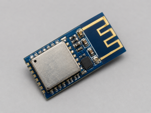
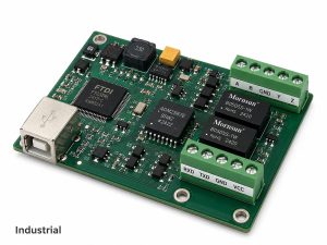
What Types of WiFi PCB and PCBA Products Need Good SNR?
Good SNR is important for many wireless products, especially when the device needs stable data transmission, long working distance, or reliable operation in a noisy environment. For PCB and PCBA projects, this often appears in products that combine WiFi modules, RF traces, antenna areas, power circuits, sensors, and control circuits on a compact board.
Common WiFi PCB and PCBA products include:
- IoT control boards
Smart controllers, wireless sensors, and connected terminals often use compact PCB layouts. Good grounding, antenna keep-out handling, and stable PCBA assembly help support reliable wireless communication. - Smart home device PCBA
Smart switches, smart plugs, gateways, lighting controllers, and home automation products need stable WiFi connection in environments with many nearby wireless devices. - Industrial wireless gateways
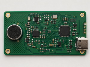
Industrial gateways, monitoring terminals, and control modules may work near motors, power supplies, relays, and metal enclosures. These products need careful PCB layout and strong manufacturing consistency. - WiFi camera and security device PCBA
WiFi cameras, access control devices, and security terminals usually require more stable data transmission. Poor SNR may lead to video delay, dropped connection, or unstable upload. - Medical and monitoring device PCBA
Wireless monitoring devices need stable communication and clean assembly quality. In these products, consistent soldering, connector reliability, and functional testing are important. - Consumer electronics with WiFi modules
Portable devices, audio products, handheld terminals, and appliance control boards may use built-in WiFi modules. The PCB layout should follow module datasheets, impedance requirements, and antenna clearance rules.
For these products, the PCB type may vary. Some use standard FR4 PCB, while compact wireless devices may need multi-layer PCB, HDI PCB, rigid-flex PCB, or impedance-controlled PCB. The final choice depends on the product size, signal speed, routing density, antenna position, power design, and assembly method.
A PCB/PCBA manufacturer can support these projects by producing the approved PCB stack-up, controlling impedance-sensitive traces, assembling WiFi modules and RF connectors, checking soldering quality, and supporting functional testing based on customer-provided requirements.

How Can PCBA Manufacturing Quality Affect WiFi Device Performance?
PCBA quality can affect WiFi performance because wireless circuits are sensitive to small production defects. A weak solder joint, shifted module, poor connector soldering, or unstable shield-can grounding may cause intermittent wireless problems.
For WiFi PCBA manufacturing, these points should be controlled carefully:
- WiFi module soldering
WiFi modules may use castellated holes, LGA pads, or fine-pitch SMT pads. Solder wetting, pad alignment, bridging, and voiding should be checked carefully. - RF connector assembly
U.FL, IPEX, SMA, and similar RF connectors need clean soldering and proper mechanical strength. A loose or misaligned connector can affect the antenna path. - Shield-can assembly
If the design includes a shield can, it should be soldered according to the customer’s drawing. Lifted corners, weak grounding, or excessive solder may reduce shielding performance. - Antenna connector handling
Small antenna connectors can be damaged by rough handling. Proper insertion, inspection, and production handling help protect the RF connection. - AOI and X-ray inspection
AOI can check placement, polarity, and visible solder quality. X-ray can help inspect hidden joints, bottom-terminated components, and some module packages. - Functional testing support
If the customer provides test firmware and test instructions, the PCBA factory can support power-on tests, module communication checks, basic wireless function checks, and other defined production tests.
A good PCB/PCBA partner should focus on repeatable manufacturing quality. The goal is not to promise complete RF tuning, but to make sure the approved design is produced and assembled consistently.
For wireless products, consistency is especially important. One good prototype is not enough. The customer needs stable soldering, controlled process parameters, traceable inspection, and reliable handling across batches.
FAQs About What Is a Good SNR for WiFi
Q1: What is a good SNR rating for WiFi?
A good SNR rating for WiFi is usually 20 dB or higher. For more stable wireless performance, 25–30 dB gives better margin.
Q2: Is SNR 15 good for WiFi?
SNR 15 is usable, but it is not ideal. It may support basic connection, but WiFi performance can become unstable when interference increases.
Q3: Is SNR 6 bad for WiFi?
Yes. SNR 6 is generally poor. The signal is too close to the noise floor, so the device may experience slow speed, packet loss, or disconnection.
Q4: Can PCB layout affect WiFi SNR?
PCB layout can influence WiFi performance by affecting RF trace quality, grounding, noise coupling, antenna keep-out, and power integrity. It does not control the full wireless environment, but poor layout can reduce the available SNR margin.
Q5: Can poor PCBA assembly reduce WiFi performance?
Yes. Poor soldering of WiFi modules, RF connectors, antenna connectors, shield cans, or ground pads can affect wireless stability. Stable SMT assembly, inspection, and functional testing help improve production consistency.

So, what is a good SNR for WiFi? In most cases, 20 dB or higher is a practical baseline, while 25–30 dB gives better stability for many wireless devices. However, WiFi performance is not decided by SNR values alone. PCB layout, grounding, controlled impedance, antenna keep-out handling, and PCBA manufacturing quality can all influence how well the wireless module performs in the final product.
For OEMs developing WiFi devices, IoT controllers, smart home products, industrial gateways, or wireless module assemblies, a reliable PCB and PCBA partner can help turn the approved design into stable production. At Best Technology, we support PCB layout execution, controlled impedance PCB manufacturing, WiFi module PCBA, PCB SMT assembly, shield-can assembly, connector soldering, AOI, X-ray inspection, and functional testing support based on customer-provided requirements.
If you have a WiFi PCB or PCBA project under development, you are welcome to send your schematic, BOM, Gerber files, stack-up, impedance requirements, and assembly instructions to sales@bestpcbs.com. Our team will review the files carefully and help you evaluate the most suitable manufacturing approach.