





A single inline package places all component leads in one straight row. Most traditional SIP components stand vertically on a PCB, allowing designers to reduce the horizontal area occupied by the package.
SIP packaging is commonly used for resistor networks, hybrid circuits, power modules, signal-conditioning devices, and some integrated circuits. It is less common in modern high-pin-count digital products, but it remains useful where a narrow footprint, through-hole retention, or several integrated passive components provide a practical advantage.
The abbreviation also requires care. SIP may mean Single Inline Package, while SiP often means System in Package. These are different packaging concepts and should not be treated as interchangeable.
What Is a Single Inline Package (SIP)?
A single inline package is an electronic component package with its pins arranged in one linear row. Traditional SIP components use through-hole leads that pass through drilled PCB holes and are soldered on the opposite side.
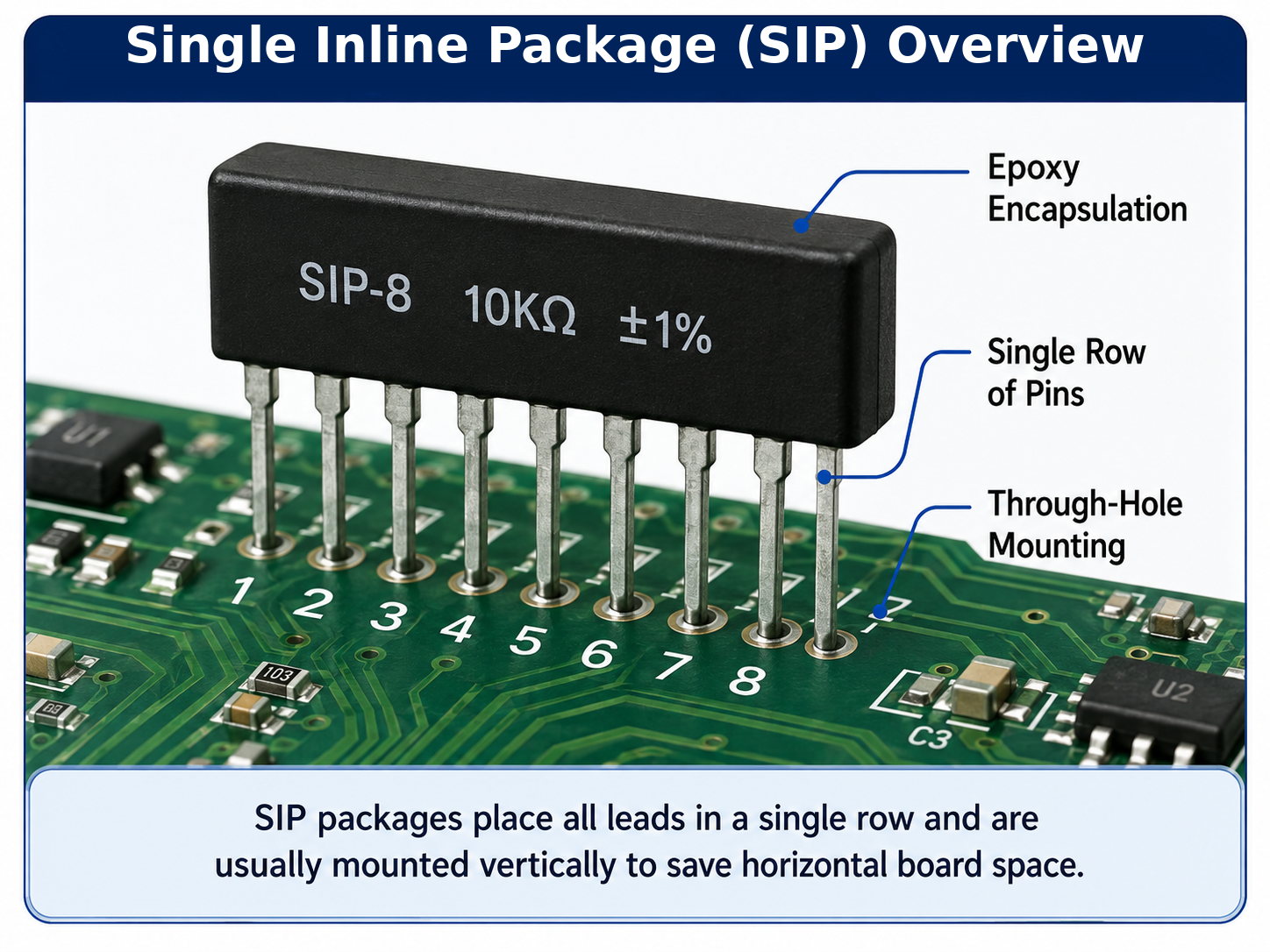
Because the body normally stands perpendicular to the PCB, the package uses little board width. The trade-off is greater component height, which can affect enclosure clearance and vibration resistance.
Common terms include:
- Single inline package
- Single in-line package
- SIP package
- Single inline pin package
- SIPP
- SIL package
A SIP package may contain one semiconductor device, multiple resistors, a hybrid circuit, or a complete power function. The name describes the external lead arrangement rather than the electrical function inside the body.
How Is a Single Inline Package Constructed?
A SIP package normally contains an internal circuit connected to a single row of metal leads. The exact construction depends on whether the part is a resistor network, semiconductor IC, hybrid module, or power device.
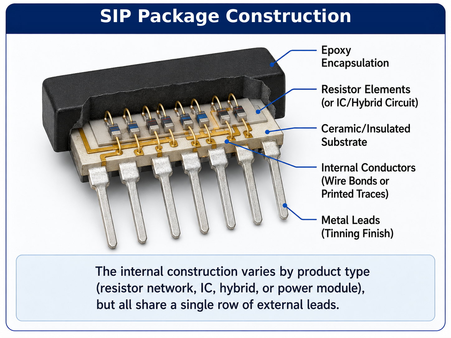
A typical package may contain:
- A semiconductor die or passive network
- A metal lead frame or internal substrate
- Wire bonds, printed conductors, or welded connections
- Plastic, epoxy, ceramic, or resin encapsulation
- Straight, formed, or staggered external leads
- A dot, notch, chamfer, or printed mark for pin 1
Thick-film resistor networks commonly use resistive elements formed on an insulated substrate and protected by a molded or coated body. Power and hybrid modules may use a ceramic substrate to support several active and passive components.
Pin pitch varies by product family. A 2.54 mm pitch is common in traditional SIP sockets and resistor networks, but designers should confirm the dimensional drawing rather than build a footprint from a visual estimate.
Package length is largely determined by pin count and lead pitch. Height varies more widely because the vertical body is part of the space-saving strategy.
What Components Use Single Inline Packages?
SIP packaging is suitable for components that require a modest number of connections and benefit from vertical installation or integrated circuitry.
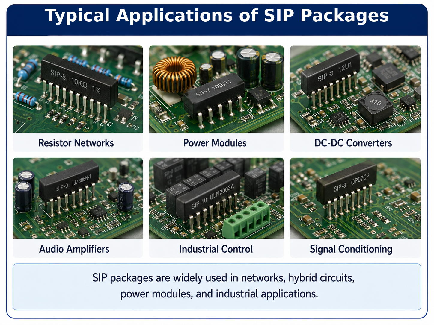
Common examples include:
- Resistor networks: Multiple resistive elements placed in one package.
- Hybrid integrated circuits: Semiconductor dies and passive components assembled on one substrate.
- Power regulator modules: Integrated switching or linear regulation functions.
- DC-DC converter modules: Input, output, control, and ground connections arranged in one row.
- Audio amplifier modules: Compact amplifier circuits used in consumer and industrial equipment.
- Transistor and diode arrays: Several related semiconductor elements in one package.
- Signal-conditioning modules: Amplification, filtering, isolation, or interface functions.
- Industrial control modules: Application-specific circuits designed for straightforward through-hole assembly.
SIP is less suitable for processors, FPGAs, and other devices requiring dozens or hundreds of connections. Those products normally use QFP, BGA, LGA, or similar high-density packages.
Buyers should also check lifecycle status. Some SIP ICs are mature or application-specific parts with limited alternatives. A design should not depend on an obsolete component unless the supply strategy and replacement plan are clear.
What Is a Single Inline Package Resistor Network?
A single inline package resistor network combines several resistors within one body. Instead of placing each resistor separately, the PCB assembler inserts one component with a single row of leads.
This arrangement can reduce PCB area, component placement count, BOM line items, purchasing workload, inspection points, and resistance variation between matched channels.
SIP resistor networks are commonly used for logic pull-ups, pull-downs, signal termination, LED current control, relay-driver interfaces, voltage dividers, and digital input conditioning.
The package appearance does not reveal the internal circuit. Two eight-pin networks may contain completely different electrical arrangements. One might have seven resistors connected to a common terminal, while another might contain four isolated resistors.
Replacement parts must therefore be selected by schematic, pinout, resistance value, tolerance, power rating, and package dimensions—not by pin count alone.
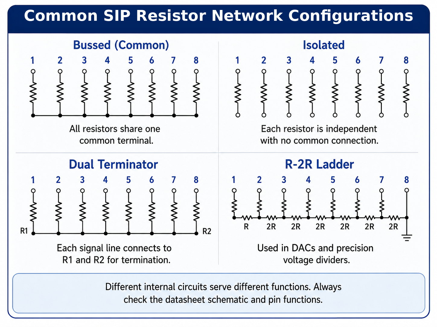
What Are the Common SIP Resistor Network Configurations?
The correct network depends on how the resistors must connect inside the circuit.
| Configuration | Internal Arrangement | Typical Application | Main Item to Verify |
|---|---|---|---|
| Bussed | One end of each resistor connects to a common pin | Pull-up, pull-down, LED current limiting | Common-pin position |
| Isolated | Each resistor has two independent terminals | Matched channels and general resistor replacement | Number of independent resistors |
| Dual terminator | Each signal connects through two resistor values | Logic-line and bus termination | Resistance pair and reference rails |
| R-2R ladder | Resistors form repeating R and 2R values | Digital-to-analog conversion | Ratio accuracy |
| RC network | Resistors and capacitors share one package | Filtering, timing, and noise suppression | Resistance, capacitance, and voltage rating |
A bussed network is efficient when several signals share a supply or ground reference. It cannot replace an isolated network unless the circuit already requires that shared connection.
For precision circuits, ratio tolerance may be more important than absolute resistance tolerance. Components formed on the same substrate often track temperature more closely than unrelated discrete resistors, but the datasheet must state the required matching performance.
What Are the Advantages and Limitations of SIP Packages?
SIP packages are most effective when a narrow footprint or integrated network provides more value than a low-profile surface-mount solution.
| Factor | Advantage | Limitation |
|---|---|---|
| PCB area | Uses a narrow strip of board space | Requires greater vertical clearance |
| Assembly | Leads are visible and easy to inspect | Requires drilled holes and a THT process |
| Mechanical retention | Through-hole leads provide strong attachment | Tall packages create more vibration leverage |
| Component integration | Can replace several separate components | One package failure may affect several functions |
| Electrical matching | Networks can provide close element matching | Internal topology reduces circuit flexibility |
| Rework | Large leads are usually accessible | Replacement parts may have limited availability |
| Production cost | Reduces placement and BOM complexity | May add a separate process to an SMT-only board |
| Pin capacity | Suitable for simple functional modules | Unsuitable for high-I/O devices |
A SIP resistor network may still be economical on a modern PCBA if it replaces many discrete components. In a fully automated SMT product, however, a surface-mount network may reduce handling and eliminate through-hole soldering.
Single Inline Package vs Dual Inline Package
The main selection question is whether the board benefits more from a narrow vertical package or a lower, mechanically balanced two-row package.
| Feature | Single Inline Package | Dual Inline Package |
|---|---|---|
| Pin arrangement | One row | Two parallel rows |
| Typical orientation | Vertical | Flat or low above the PCB |
| PCB width | Narrow | Wider |
| Component height | Usually higher | Usually lower |
| Mechanical support | Concentrated along one row | Distributed across two rows |
| Pin capacity | Low to moderate | Moderate |
| Socket availability | Product-specific | Widely available for standard DIP sizes |
| Common applications | Resistor networks, hybrid circuits, power modules | Logic ICs, op-amps, controllers, memory |
A SIP package is useful when board width is restricted. DIP is often preferable when socketing, standardized dimensions, lower height, or stronger two-sided mechanical support is required.
Single Inline Package vs Small Outline Package
A traditional SIP is normally a through-hole package, while a small outline package is designed for surface-mount assembly.
| Feature | SIP | SOP |
|---|---|---|
| Lead arrangement | One row | Two opposite rows |
| Assembly type | Usually through-hole | Surface mount |
| PCB drilling | Required | Not required |
| Body orientation | Usually vertical | Flat |
| Component height | Higher | Lower |
| Assembly process | Wave, selective, or manual soldering | Solder paste, placement, and reflow |
SOP is generally better for compact, high-volume SMT production. SIP remains appropriate when a through-hole module, resistor network, or vertical package provides a specific electrical or mechanical advantage.
Single Inline Package vs Quad Flat Package
QFP packages distribute leads around four sides, allowing many more electrical connections than a single-row package.
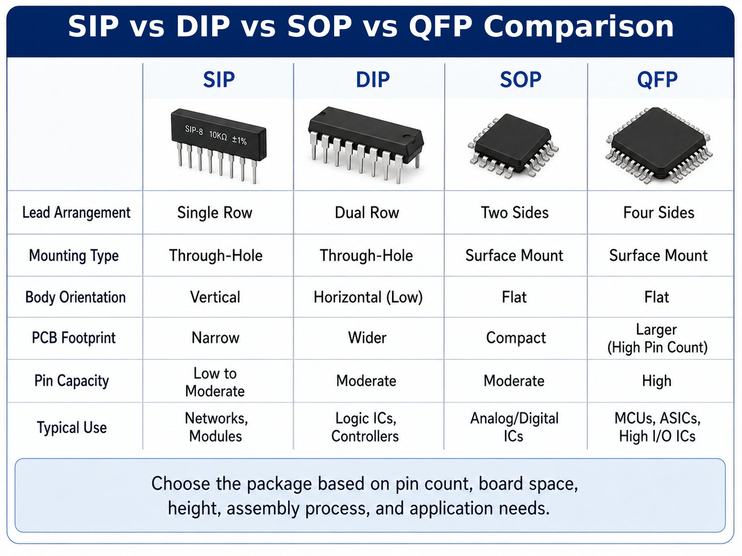
| Feature | SIP | QFP |
|---|---|---|
| Lead locations | One side | Four sides |
| Pin density | Low to moderate | Moderate to high |
| Mounting method | Usually through-hole | Surface mount |
| Body orientation | Vertical | Flat |
| Routing complexity | Relatively simple | Higher due to dense lead distribution |
| Typical devices | Networks, hybrid circuits, power modules | Microcontrollers, ASICs, interface ICs |
QFP is the practical choice when an IC needs many signal, power, and ground pins. SIP is better suited to simpler functions where one linear row provides enough connections.
Single Inline Package vs System in Package: Why Does SIP Have Two Meanings?
Single Inline Package and System in Package describe different features.
A Single Inline Package describes how the external leads are arranged. The component has one row of pins and is often mounted vertically through the PCB.
A System in Package, commonly written as SiP, describes the integration of several semiconductor dies or functional blocks inside one package. A SiP may combine a processor, memory, RF circuitry, sensors, and passive components.
| Term | Meaning | What It Describes | Example |
|---|---|---|---|
| SIP or SIPP | Single Inline Package | External pin arrangement | Resistor network or power module |
| SiP | System in Package | Internal functional integration | Processor and memory in one package |
Datasheets and distributor listings do not always use capitalization consistently. Buyers should specify the full package name, exact manufacturer part number, and package drawing when requesting a component or PCBA quotation.
How Do You Read a SIP Package Datasheet and Pinout?
The footprint should be created from the mechanical drawing rather than from a photograph or measured sample.
Review these items before PCB layout:
- Pin count: Confirm the number of physical leads and any omitted positions.
- Pin pitch: Check the center-to-center spacing.
- Lead dimensions: Review lead width, thickness, shape, and tolerance.
- Body dimensions: Use maximum length, width, and height values.
- Stand-off: Determine how far the body sits above the PCB.
- Pin 1 mark: Look for a dot, notch, chamfer, stripe, or molded feature.
- Internal schematic: Verify bussed, isolated, terminated, or functional connections.
- Electrical ratings: Check voltage, current, resistance, power, and insulation.
- Tolerance: Separate absolute tolerance from element-to-element matching.
- Temperature rating: Review operating, storage, and soldering limits.
- Derating curve: Confirm how allowable power changes with temperature.
- Ordering suffix: Check lead finish, package profile, tolerance, and packing method.
For resistor networks, the internal schematic is essential. A shared terminal may appear at pin 1, the last pin, or another location depending on the series.
What Should PCB Designers Consider for SIP Footprints and Assembly?
A reliable SIP footprint must account for lead tolerance, plated-hole size, annular ring, component height, soldering method, and mechanical loading.
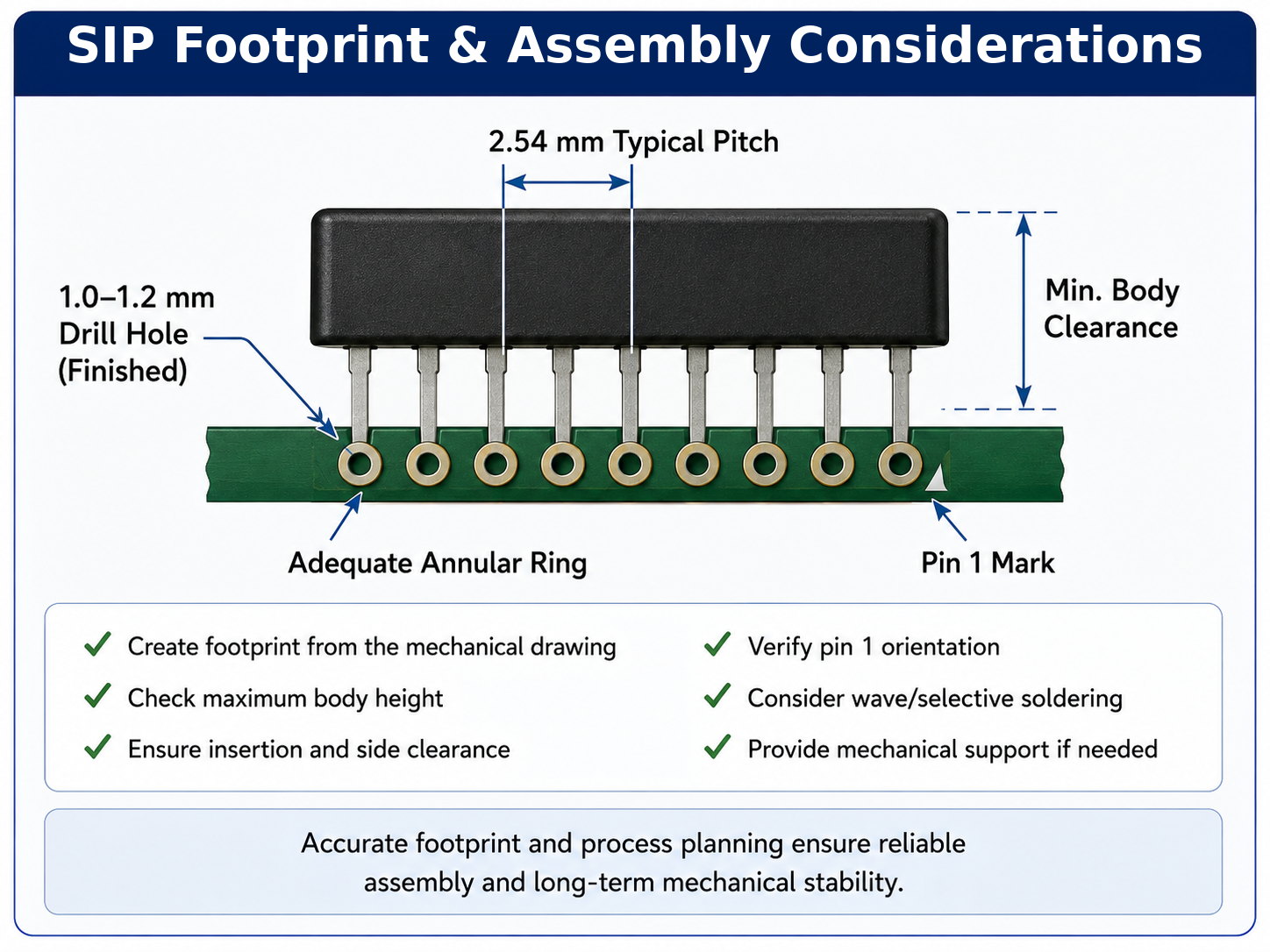
The finished-hole diameter should provide enough clearance for the component’s maximum lead dimensions while remaining compatible with the PCB fabricator’s drilling and plating tolerances. Avoid copying the nominal lead width directly into the drill size.
Important layout and assembly checks include:
- Create the footprint from the manufacturer’s mechanical drawing.
- Confirm whether dimensions are stated in inches or millimeters.
- Mark pin 1 on both the silkscreen and assembly drawing.
- Provide enough annular ring for drill registration and plating.
- Check the maximum package height against the enclosure.
- Leave side clearance for insertion and rework.
- Keep the body away from connectors, shielding cans, and board stiffeners.
- Verify lead protrusion on the solder side.
- Add support for tall or heavy modules used in vibration environments.
- Confirm compatibility with wave, selective, or manual soldering.
Tall modules deserve additional attention in automotive, industrial, railway, and heavy-equipment electronics. Their mass can create leverage at the solder joints during vibration. Adhesive support, retaining clips, shorter leads, or a lower-profile alternative may be required.
For PCBA quotation, EBest Circuit normally needs the Gerber files, NC drill data, BOM, assembly drawings, and component information. Centroid data is also required for SMT components on a mixed-technology board. The company’s PCB assembly FAQ explains the broader file and process requirements. Providing the SIP datasheet helps engineers verify orientation, hole dimensions, height, and soldering requirements before production.
How Do You Choose the Right SIP Package for a PCB or PCBA?
Start with the electrical function. Then evaluate mechanical compatibility, manufacturing cost, and supply continuity.
Confirm the internal circuit. For a resistor network, determine whether the design requires bussed, isolated, dual-terminator, ladder, or RC connections. For an IC or module, compare every pin function.
Check the electrical ratings. Review voltage, current, resistance, power, tolerance, temperature coefficient, insulation, and operating temperature. Apply the manufacturer’s derating requirements.
Evaluate board and enclosure space. A SIP package saves horizontal area but requires more vertical clearance. Use maximum body dimensions rather than typical values.
Match the assembly process. A SIP component adds little complexity when the board already contains through-hole connectors or transformers. On an otherwise all-SMT assembly, it may require manual insertion, selective soldering, or an additional production stage. Review the available through-hole assembly service when planning insertion, soldering, inspection, and mixed-technology production.
Review mechanical conditions. Consider package mass, body height, lead length, PCB thickness, support points, vibration, and shock.
Check supply continuity. Confirm lifecycle status, manufacturer lead time, minimum order quantity, authorized distribution, and second-source availability.
Compare total installed cost. A resistor network may cost more than one discrete resistor but still lower the total cost when placement, inspection, purchasing, and inventory are included.
A useful PCB or PCBA quotation package should include:
- Gerber files
- NC drill files
- BOM with manufacturer part numbers
- Assembly drawings
- Pick-and-place data
- SIP component datasheet
- Prototype and volume quantities
- Soldering requirements
- Inspection and testing requirements
- Approved substitution rules
Prototype assembly is particularly useful when a SIP component is tall, heavy, obsolete, manually formed, or based on an unusual pitch. The prototype should verify fit, polarity, solder fill, enclosure clearance, mechanical stability, and rework access.
FAQs About Single Inline Packages
1. What does SIP stand for in electronic packaging?
SIP commonly stands for Single Inline Package when describing a component with one row of pins. SiP may also mean System in Package in semiconductor-integration discussions.
2. Is a SIP package always a through-hole package?
Most traditional SIP components are through-hole devices. Some specialized products may use formed or surface-compatible leads, so the manufacturer’s recommended footprint should be checked.
3. What is a single inline package resistor?
It is a package containing several resistors. The elements may share a common terminal, remain isolated, or form a termination or ladder network.
4. What is the difference between SIP and DIP?
SIP uses one row of pins and usually stands vertically. DIP uses two parallel rows and normally has a lower, wider body.
5. Is SIP the same as System in Package?
No. Single Inline Package describes the external lead arrangement. System in Package describes several functional devices integrated inside one package.
6. What is the typical pin spacing of a SIP package?
A 2.54 mm pitch is common in traditional SIP products, but other pitches exist. The exact spacing must come from the mechanical drawing.
7. How do you identify pin 1 on a SIP component?
Pin 1 may be identified by a dot, notch, stripe, chamfer, molded feature, or different lead shape. The datasheet should provide the official orientation.
8. Are SIP packages still used in modern electronics?
Yes. They remain useful in resistor networks, power modules, hybrid circuits, industrial controls, and products that benefit from through-hole retention or a narrow footprint.
9. Can a SIP component be replaced with an SOP component?
Not directly. The PCB footprint, pinout, package height, thermal behavior, and assembly process are different. A board redesign or adapter may be necessary.
10. What PCB files are needed to assemble a SIP component?
The assembler normally needs Gerber files, drill data, a BOM, assembly drawings, and the component datasheet. Mixed SMT and through-hole boards also require pick-and-place data for the SMT components.
Conclusion
A single inline package provides a narrow PCB footprint, accessible through-hole connections, and an efficient way to integrate resistor networks or functional modules. Its main trade-offs are greater component height, limited pin capacity, additional through-hole processing, and possible sourcing constraints for older parts.
Before selecting a SIP component, verify its internal circuit, pinout, lead pitch, maximum height, soldering method, mechanical support, and lifecycle status. Complete component and PCB documentation also helps prevent footprint and orientation errors during prototype assembly.
For support with SIP footprint review, PCB fabrication, prototype PCBA, or mixed SMT and through-hole assembly, contact EBest Circuit at sales@bestpcbs.com.







