MCPCB VS Regular PCB is a topic many engineers and buyers search when choosing the right board for a project. Each type has clear benefits depending on the application, environment, and performance needs. Choosing between them needs more than just looking at the price. It also depends on thermal needs, material selection, and the product’s lifespan.
In this blog, we’ll explore the core differences between MCPCB VS Regular PCB, focusing on materials, design, thermal resistance, and common applications. We’ll also highlight why metal core boards have become more popular for LED lighting and other heat-sensitive uses.
What is the most basic circuit board?
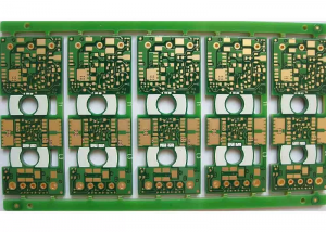
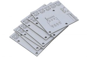
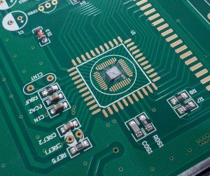
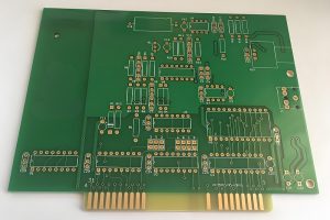
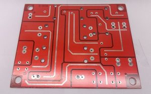
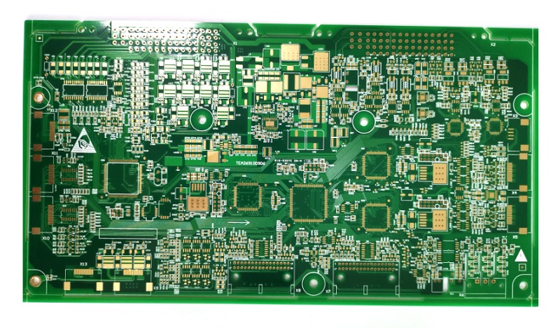
The most basic circuit board used today is the FR4 PCB. FR4 refers to the fiberglass-reinforced epoxy laminate used as the core. This type of board acts as a solid foundation for electrical components. It supports the copper traces that carry signals across the board. FR4 has been the industry standard for decades due to its balanced electrical, mechanical, and thermal properties.
Most everyday electronics, from home appliances to industrial equipment, rely on FR4 PCBs because of their low cost, stable structure, and easy processing.
What is MCPCB?
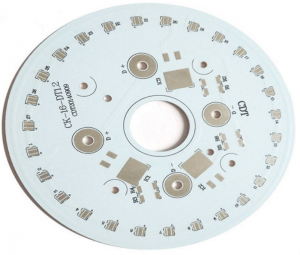
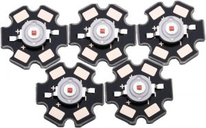
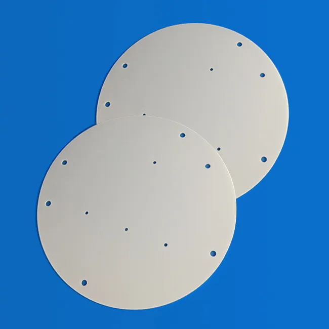
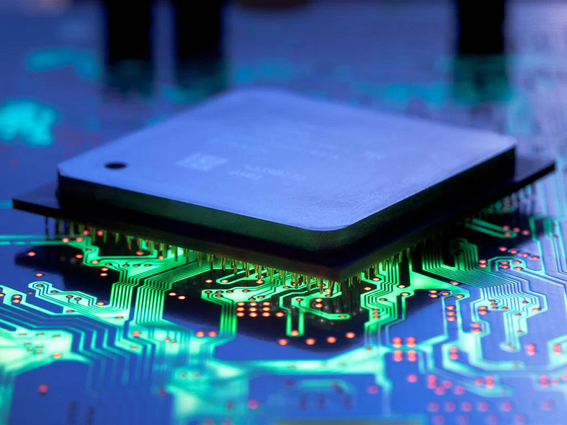
MCPCB stands for Metal Core Printed Circuit Board. Instead of a fiberglass base, these boards use a metal core layer, usually aluminum or copper. This design helps the board handle high heat better than regular FR4 boards.
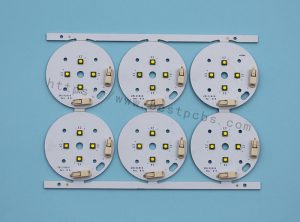
In MCPCB design, the metal core sits under the circuit layers. It helps pull heat away from hot components like LEDs or power transistors. This cooling method reduces the chance of overheating, extending the life of the whole board. MCPCB LED applications are some of the most common, especially in automotive, industrial, and high-power LED lighting.
What is the material of MCPCB?
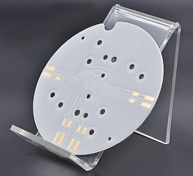
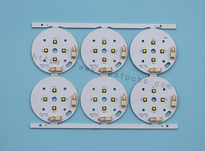
The core material used in MCPCB design is usually aluminum or copper. Aluminum is more common due to its good heat conductivity and affordable cost. It balances performance and price, making it a top choice for MCPCB LED boards.
Copper has higher thermal conductivity, but its cost is much higher. That’s why copper-core MCPCBs are mainly found in high-end equipment or where heat management is critical. On top of the metal core, dielectric layers provide electrical insulation and guide heat to the core. Copper traces on top complete the circuit.
Why is FR4 used in PCB?
FR4 remains popular in regular FR4 PCBs for many reasons. It has good mechanical strength, supports multi-layer designs, and offers decent thermal stability for common electronics. It also resists moisture well, making it reliable in humid environments.
Another reason FR4 PCBs are used widely is their low manufacturing cost. They work well for low-power circuits where high heat dissipation isn’t a serious issue. For most general electronics, FR4 boards provide all the needed performance at a low price.
What are the thermal issues with PCB?
Regular FR4 PCBs struggle when components produce high heat. Since fiberglass does not spread heat well, hot spots form near high-power parts. Over time, this localized heat can damage components, weaken solder joints, or deform the board itself.
This thermal problem becomes more serious in high-density layouts where heat has nowhere to escape. That’s why high-power LED lighting, power converters, and some automotive systems have switched to MCPCB design.
What is the thermal resistance of MCPCB?
MCPCB thermal resistance is much lower than regular PCBs. This low resistance means heat can move through the board faster, keeping temperatures under control.
In a well-designed MCPCB, heat moves directly from the component through the dielectric layer into the metal core, where it spreads across a larger area. This process reduces hot spots, protects components, and extends the product’s lifespan. Compared to regular FR4 boards, MCPCBs handle thermal stress far better.
What are the uses of MCPCB?
MCPCB design works best for products where heat dissipation matters most. Common uses include:
High-power LED lighting, especially in automotive headlights and streetlights.
Power supplies where voltage conversion creates heat.
Solar inverters, handling high current and constant power flow.
Telecom equipment, where stable performance under heat matters.
Automotive control systems, especially in engine bays.
Because of their thermal handling skills, MCPCB LED boards are some of the most common in today’s market.
What are the advantages of metal core PCB?
MCPCB design offers many advantages over regular PCBs. They include:
Superior heat management, extending product life.
Better mechanical strength, reducing vibration damage.
Compact layouts, reducing weight and size.
Reliable thermal paths, protecting sensitive parts.
Stronger durability in tough environments.
For projects where heat is a real issue, MCPCBs provide solutions that FR4 PCBs cannot match.
What are the disadvantages of PCB?
While FR4 PCBs work well for many products, they do have some limits in high-heat conditions. These boards:
Do not spread heat well, leading to hot spots.
May soften under high heat, reducing long-term stability.
Offer weaker thermal paths, limiting high-power designs.
However, for low-power and general devices, FR4 PCBs still provide affordable, reliable performance.
What is the difference between FR4 and MCPCB?
When comparing MCPCB VS Regular PCB, What are Differences? The biggest difference comes down to thermal performance. MCPCBs use metal cores, usually aluminum or copper, to spread heat faster and protect components.
Regular FR4 PCBs rely on fiberglass, which does not move heat well. This makes them better for low-power circuits, where thermal buildup is not a concern.
Cost is another difference. FR4 PCBs cost less to produce, especially in mass production. But for products where heat is a risk, spending more on MCPCB design reduces failure rates, protects components, and lowers maintenance costs.
In short, MCPCB VS Regular PCB is not just about cost. It’s about matching the board to the product’s real-world needs.
In a nutshell, in the world of MCPCB VS Regular PCB, there’s no one-size-fits-all answer. FR4 PCBs remain the first choice for low-power electronics due to their low cost and easy manufacturing process. But when heat handling matters, especially for LED lighting, power electronics, or automotive systems, MCPCB design offers the best protection.
At EBest Circuit (Best Technology), we specialize in custom MCPCB design, high-quality FR4 PCBs, and tailored thermal solutions. With over 18 years of experience, we help customers select the right PCB for each project. Whether you need reliable FR4 boards or advanced metal core solutions, our team provides fast support, expert advice, and global delivery. Please feel free to reach out to EBest Circuit (Best Technology) at sales@bestpcbs.com for your needs related to MCPCB and regular PCB.