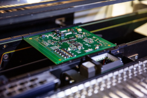
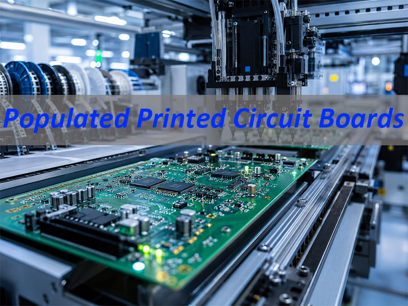
For professional electronics buyers, populated printed circuit boards are more than assembled boards with components soldered on them. They are production-ready PCBAs that must meet design intent, component sourcing requirements, soldering reliability, test standards, delivery schedules, and final product performance. A project may start with a Gerber file and BOM, but turning it into a stable PCBA requires engineering review, PCB fabrication control, component verification, SMT assembly, through-hole soldering, inspection, testing, and production documentation.
Best Technology provides custom populated printed circuit boards services from prototype to production. We support bare PCB manufacturing, component sourcing, PCB SMT assembly, DIP assembly, mixed assembly, AOI inspection, X-ray inspection, functional testing, packaging, and global delivery. For prototypes, low-volume builds, and batch production, our team helps customers reduce handover risks and keep the PCB-to-PCBA process under one coordinated system. For project review or quotation, please send your Gerber files, BOM, pick-and-place file, assembly drawing, quantity, and testing requirements to sales@bestpcbs.com.
What Are Populated Printed Circuit Boards?
Populated printed circuit boards are PCBs that already have electronic components mounted and soldered onto the board. These components may include resistors, capacitors, ICs, connectors, relays, LEDs, sensors, transformers, switches, and other parts required by the product design.
In practical engineering and purchasing communication, populated printed circuit boards are also called:
- Populated PCBs
- Assembled PCBs
- PCBAs
- PCB with components
- Printed circuit board assemblies
A bare PCB is only the foundation. It contains copper traces, pads, vias, solder mask, silkscreen, and surface finish, but it cannot perform the final electronic function alone. After components are installed and soldered, the board becomes a functional electronic assembly.
For professional customers, the key difference is not only terminology. The real difference is responsibility.
| Item | Bare PCB | Populated PCB / PCBA |
|---|---|---|
| Component status | No components | Components mounted and soldered |
| Function | Cannot work alone | Can be tested and used in a device |
| Supplier scope | PCB fabrication only | PCB fabrication + assembly + inspection |
| Main risk | Material, stack-up, copper, drilling | BOM, soldering, polarity, testing, function |
| Buyer focus | Board quality | Full assembly reliability |
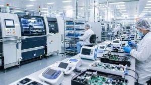
A populated PCB project usually involves more coordination than a bare PCB order. The supplier needs to understand the PCB design, BOM accuracy, part availability, assembly process, inspection requirements, and final test method. This is why many professional buyers prefer a manufacturer that can manage both PCB fabrication and PCBA assembly.
Custom Populated PCB Assembly Services We Offer
Best Technology provides custom populated PCB assembly services for customers who need more than basic component soldering. Our service is designed for projects that require controlled manufacturing, flexible order quantities, engineering communication, and reliable delivery.
Our populated PCB services include the following major areas:
1. Bare PCB Fabrication
We can manufacture the bare circuit board before assembly, which helps reduce mismatch between PCB production and assembly requirements.
We support:
- FR4 PCB
- HDI PCB
- Rigid-flex PCB
- Flexible PCB
- Aluminum PCB
- Copper base PCB
- Ceramic PCB
- Heavy copper PCB
- High Tg PCB
- Impedance control PCB
- Multilayer PCB
- Special surface finish PCB
This is useful when your populated circuit boards require special materials, controlled impedance, high-current design, thermal management, or compact routing.
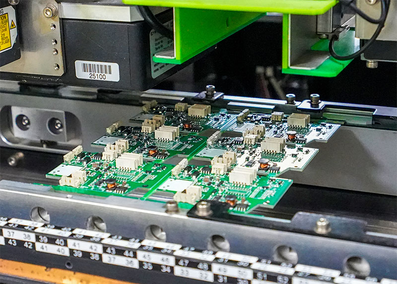
2. SMT Assembly
SMT assembly is used for surface-mount components and high-density PCB designs. It is suitable for compact boards, automated production, and modern electronic products.
We support:
- Resistors and capacitors
- Diodes and LEDs
- ICs and controllers
- QFN, QFP, SOP, SOT packages
- BGA assembly
- Fine-pitch components
- Sensors and communication modules
- Small passive components
For dense PCBA projects, SMT process control is critical. Solder paste printing, placement accuracy, reflow profile, and AOI inspection all affect final board reliability.
3. Through-Hole Assembly
Some populated PCBs still require through-hole components because of mechanical strength, high current, or connector durability.
Common through-hole components include:
- Pin headers
- Terminal blocks
- Transformers
- Relays
- Large capacitors
- Connectors
- Switches
- Power components
- Mechanical support parts
Through-hole assembly may involve manual soldering, wave soldering, or selective soldering, depending on the design and production quantity.
4. Mixed Assembly
Many custom populated printed circuit boards use both SMT and through-hole parts. These projects need a clear process route because the board may pass through several assembly stages.
A typical mixed assembly project may include:
- Solder paste printing
- SMT placement
- Reflow soldering
- AOI inspection
- Through-hole insertion
- Wave soldering or manual soldering
- Final inspection
- Functional testing
Mixed assembly is common in industrial control boards, power supply boards, LED driver boards, communication modules, and automotive electronic modules.
5. Component Sourcing
For turnkey populated PCB projects, we can source components according to the customer’s BOM.
Our sourcing support includes:
- Manufacturer part number checking
- Package verification
- Quantity confirmation
- Availability review
- Lead time checking
- Alternative part suggestion
- Obsolete component warning
- Customer approval before substitution
Component sourcing is one of the most important parts of populated PCB production. A wrong package, wrong voltage rating, wrong tolerance, or unapproved substitute can create serious production issues. That is why BOM review is completed before assembly starts.
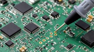
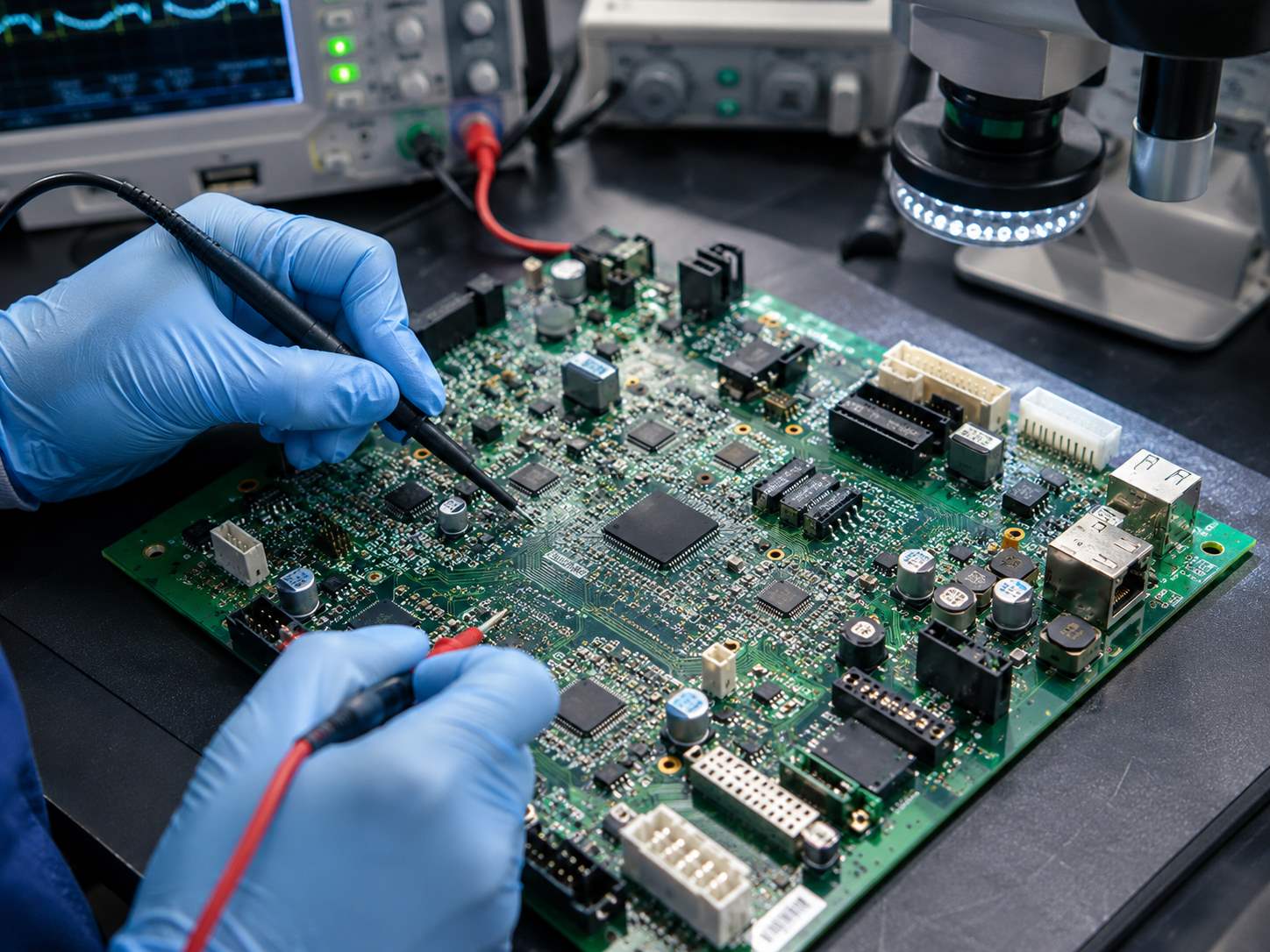
6. Inspection and Testing
Inspection and testing are not optional details. They are part of the production strategy.
Depending on project requirements, we can support:
- Visual inspection
- AOI inspection
- X-ray inspection
- First article inspection
- ICT
- Flying probe testing
- Functional testing
- Customer-specific test procedure
- Final quality report
For BGA, QFN, and other hidden-joint packages, X-ray inspection is especially useful because the solder joints cannot be fully checked by visual inspection alone.
7. Packaging and Delivery
Finished populated PCBs need proper packaging to avoid damage during transportation.
Packaging can be arranged based on:
- Component height
- Board size
- Connector position
- Moisture sensitivity
- ESD requirements
- Quantity per carton
- Customer labeling requirements
- Export shipping method
For professional customers, good packaging is part of quality control. A board that passes testing still needs to arrive safely.
How We Build Populated PCBs from Bare Boards?
A reliable populated PCB is not created by one assembly step. It is built through a controlled production chain. At Best Technology, the process starts with engineering review and continues through PCB fabrication, component preparation, assembly, inspection, testing, and shipment.
The typical build process includes:
1. Engineering File Review
Before production, our engineering team reviews the files provided by the customer.
We check:
- Gerber file completeness
- PCB stack-up and material notes
- BOM accuracy
- Component package matching
- Polarity marks
- Pick-and-place coordinates
- Assembly drawing notes
- Special soldering requirements
- Testing requirements
This step helps identify possible problems before they enter production. For example, a mismatch between BOM package and PCB footprint can delay assembly or cause wrong placement. A missing polarity mark can create functional failure. A connector direction issue can affect final enclosure installation.
2. PCB Fabrication Preparation
Once the PCB data is confirmed, the bare board is manufactured according to the project specification.
Key points include:
- Material selection
- Copper thickness
- Board thickness
- Layer count
- Surface finish
- Solder mask color
- Silkscreen clarity
- Hole tolerance
- Impedance control, if required
- Panelization for assembly
For populated printed circuit boards, PCB fabrication must consider later assembly needs. Pad quality, surface finish, solder mask registration, and panel design all affect SMT performance.
3. Component and BOM Verification
Before assembly, components are checked against the BOM.
We review:
- Part number
- Package type
- Quantity
- Polarity
- Moisture sensitivity
- Storage condition
- Substitute approval
- Customer-supplied parts, if any
This is especially important for turnkey and hybrid projects. When parts are sourced by the manufacturer, clear approval rules help prevent wrong substitutions.
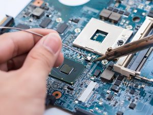
4. SMT Assembly
The SMT PCB assembly process includes solder paste printing, component placement, and reflow soldering.
Key control points include:
- Stencil design
- Solder paste volume
- Printing alignment
- Placement accuracy
- Reflow temperature profile
- Component shift control
- Tombstone prevention
- Solder bridge prevention
For fine-pitch ICs, BGA, QFN, small passive parts, LEDs, and thermal pads, SMT process control directly affects production yield.
5. Through-Hole and Manual Assembly
If the board includes through-hole or mechanical components, they are assembled after SMT or according to the planned route.
This stage may include:
- Manual insertion
- Manual soldering
- Wave soldering
- Selective soldering
- Connector alignment check
- Mechanical fit check
Professional handling is important because through-hole parts often face mechanical stress during product installation.
6. Inspection and Testing
After assembly, populated PCBs are inspected and tested according to project needs.
Common inspection steps include:
- AOI for SMT defects
- X-ray for BGA and QFN solder joints
- Visual inspection for connectors and through-hole parts
- First article inspection for new projects
- Functional testing based on customer test procedure
The purpose is not only to find defects. It is to confirm that the board is ready for customer validation or final use.
Turnkey and Consigned Options for Populated PCB Projects
Professional customers often have different supply chain strategies. Some prefer a complete turnkey service. Others want to provide key components themselves. Best Technology supports both options.
Option 1: Turnkey Populated PCB Service
In turnkey service, we manage the full production chain.
This can include:
- PCB fabrication
- Component sourcing
- BOM review
- SMT assembly
- Through-hole assembly
- Inspection
- Testing
- Packaging
- Shipment
Turnkey service is suitable for customers who want fewer suppliers and smoother coordination.
It is especially useful when:
- The BOM contains many standard parts
- The customer wants to reduce purchasing workload
- The project needs faster supplier communication
- PCB and assembly should be coordinated together
- The customer needs prototype-to-production support
The main advantage is efficiency. Instead of managing PCB supplier, component supplier, assembly factory, and testing partner separately, the customer can work with one manufacturing team.
Option 2: Consigned Assembly
In consigned assembly, the customer provides all or part of the components. We handle the PCB fabrication and assembly work based on the provided materials and production files.
Consigned assembly is suitable when:
- The customer already has approved components
- Some ICs are customer-controlled
- Certain parts are expensive or difficult to source
- The customer has existing supplier agreements
- Components require programming before assembly
- The customer wants strict control over key parts
Before production, we check the received components and confirm quantity, packaging, and condition.
Option 3: Hybrid Assembly
Many projects use a hybrid model. The customer provides key ICs, programmed parts, or special components, while we source standard passive components, connectors, and common parts.
This option gives customers both control and flexibility.
| Service Model | Best For | Customer Provides | Best Technology Handles |
|---|---|---|---|
| Turnkey | Full project outsourcing | Design files and BOM | PCB, parts, assembly, testing |
| Consigned | Customer-controlled components | Components and files | Assembly and inspection |
| Hybrid | Mixed sourcing strategy | Key parts | Common parts, PCB, assembly |
The right choice depends on cost, lead time, component risk, and internal purchasing policy.
Prototype Populated PCB Services for Design Validation
Prototype populated PCBs are used to verify the design before batch production. This stage is important because it helps customers find design, assembly, sourcing, and testing issues early.
For professional projects, prototype production is not simply “making a few samples.” It is a risk-control step before larger investment.
What Prototype Builds Help Validate
A prototype populated PCB can help check:
- Circuit function
Confirm whether the board performs as designed. - Component package matching
Check whether BOM parts match PCB footprints. - Polarity and orientation
Verify LEDs, diodes, ICs, electrolytic capacitors, and connectors. - Mechanical fit
Confirm connector direction, component height, enclosure fit, and mounting holes. - Thermal behavior
Check whether heat-generating components need layout or material adjustment. - Assembly feasibility
Identify soldering risks, stencil issues, fine-pitch challenges, or manual assembly concerns. - Testing method
Confirm how the board should be powered, measured, programmed, and validated.
How We Support Prototype Projects
For prototype populated printed circuit boards, we can support:
- Small-batch PCB fabrication
- Quick SMT assembly
- Through-hole assembly
- Engineering file review
- DFM and DFA feedback
- First article inspection
- Functional testing support
- Production notes for next batch
The prototype stage also helps prepare for pilot production. Once the prototype is approved, we can improve stencil design, assembly route, test plan, packaging method, and production documentation for repeat orders.
This is valuable for R&D teams, startups, OEM brands, hardware companies, industrial product developers, and customers preparing for mass production.
Quality Control for Populated Printed Circuit Boards
Quality control for populated printed circuit boards must cover the full process. A board can fail because of PCB defects, wrong components, poor soldering, incorrect polarity, weak connectors, insufficient testing, or packaging damage. A reliable manufacturer must control each stage.
At Best Technology, quality control is divided into several layers.
1. PCB Quality Control
Before assembly, the bare PCB must meet the design specification.
We check:
- Board dimension
- Hole quality
- Surface finish
- Solder mask
- Silkscreen
- Pad condition
- Warpage
- Panel quality
- Electrical performance, if required
PCB quality affects assembly quality. Poor pad finish or board warpage can create soldering issues.
2. Component Quality Control
Components are checked before production.
Important checks include:
- Correct part number
- Correct package
- Correct quantity
- Moisture sensitivity
- Visible damage
- Polarity
- Storage condition
- Customer approval for substitutes
This step reduces the risk of wrong assembly and functional failure.
3. SMT Process Control
During SMT assembly, solder paste printing and placement accuracy are controlled carefully.
Key inspection points include:
- Solder paste coverage
- Component alignment
- Missing parts
- Polarity direction
- Solder bridges
- Tombstoning
- Fine-pitch solder quality
AOI inspection is widely used after reflow soldering.
4. X-Ray Inspection for Hidden Solder Joints
For BGA, QFN, LGA, and some bottom-terminated components, solder joints are hidden under the package. X-ray inspection helps check:
- Solder ball alignment
- Bridging
- Voiding
- Open joints
- Insufficient solder
- Short circuits
This is important for high-density and high-reliability populated PCBs.
5. Functional Testing
Functional testing checks whether the assembled board works according to the customer’s requirement.
Testing may include:
- Power-on test
- Voltage and current check
- LED indicator check
- Signal input/output test
- Communication test
- Firmware or programming check
- Load test
- Customer test fixture operation
For complex products, the customer may provide a test procedure or test fixture. We can follow the approved method during production.
6. Final Inspection and Packaging Check
Before shipment, final inspection confirms:
- Board appearance
- Labeling
- Quantity
- Packaging method
- Connector protection
- ESD protection
- Carton information
- Shipment documents
This final step helps ensure that the boards arrive in usable condition.
Custom Populated PCB Types We Can Build
Different electronic products need different PCB structures. Best Technology supports various populated PCB types for prototype, low-volume, and batch production projects.
1. FR4 Populated PCBs
FR4 populated PCBs are widely used in consumer electronics, industrial control, communication devices, power modules, and general electronic products.
They are suitable for:
- Control boards
- Sensor boards
- Communication modules
- Smart home devices
- Industrial controllers
- General PCBA projects
FR4 offers a practical balance of cost, mechanical strength, and electrical performance.
2. HDI Populated PCBs
HDI populated PCBs are used when the product needs compact size and high routing density.
They are suitable for:
- Portable electronics
- Communication devices
- Medical instruments
- High-density control modules
- Products using small BGAs or fine-pitch ICs
HDI projects require strong coordination between PCB fabrication and assembly because pad size, via structure, and component density are more demanding.
3. Rigid-Flex Populated PCBs
Rigid-flex populated PCBs combine rigid board areas and flexible circuits. They are useful when the product has limited space or needs folding installation.
They are suitable for:
- Wearable devices
- Medical electronics
- Compact instruments
- Camera modules
- Aerospace electronics
- Complex mechanical designs
Rigid-flex assembly needs careful handling because the flexible area can be damaged by stress or incorrect fixture design.
4. Aluminum Populated PCBs
Aluminum populated PCBs are used when thermal dissipation is important.
They are suitable for:
- LED lighting
- Power modules
- Motor control
- Automotive lighting
- High-power driver boards
The metal base helps move heat away from components, improving thermal stability.
5. Ceramic Populated PCBs
Ceramic populated PCBs are used in high-power, high-temperature, high-frequency, and high-reliability applications.
Common ceramic materials include:
- Alumina
- Aluminum nitride
- Silicon nitride
They are suitable for:
- Power electronics
- Laser modules
- Medical devices
- RF applications
- EV power modules
- High-thermal-demand products
Ceramic PCB assembly requires proper process control because the substrate and metallization structure differ from standard FR4 boards.
6. Heavy Copper Populated PCBs
Heavy copper populated PCBs are designed for higher current applications.
They are suitable for:
- Battery systems
- Power control boards
- Industrial equipment
- Energy storage systems
- High-current modules
Heavy copper boards need careful thermal and soldering consideration during assembly.
7. Impedance Control Populated PCBs
Impedance control populated PCBs are used for high-speed and signal-sensitive applications.
They are suitable for:
- RF products
- Communication equipment
- High-speed digital modules
- Data transmission boards
- Signal control devices
These projects require controlled stack-up, trace width, dielectric thickness, and manufacturing tolerance.
Files Needed for a Populated PCB Quote
A clear quote depends on clear technical files. When customers request a populated PCB quote, incomplete information may cause delays or inaccurate pricing. To help us quote quickly and correctly, please prepare the following files.
1. Gerber Files
Gerber files define the PCB manufacturing data.
They should include:
- Copper layers
- Solder mask
- Silkscreen
- Drill data
- Board outline
- Surface finish notes
- Panel information, if available
For special boards, please also provide material, thickness, copper weight, impedance, and stack-up requirements.
2. BOM
The BOM is one of the most important files for populated printed circuit boards.
A complete BOM should include:
- Reference designator
- Component value
- Package
- Manufacturer part number
- Brand or manufacturer
- Quantity
- Description
- Approved alternatives, if allowed
- Do-not-substitute parts, if any
A clear BOM helps avoid wrong components and speeds up sourcing.
3. Pick-and-Place File
The pick-and-place file is also called a centroid file or CPL file.
It should include:
- Component coordinates
- Rotation
- Placement side
- Reference designators
This file is used for SMT programming.
4. Assembly Drawing
The assembly drawing helps confirm component orientation and mechanical details.
It may include:
- Polarity marks
- Connector direction
- Component height notes
- Manual soldering notes
- Mechanical installation notes
- Special assembly instructions
For complex boards, a 3D file is also helpful.
5. Testing Requirements
If functional testing is needed, please provide a clear test method.
Useful information includes:
- Input voltage
- Output requirement
- Current limit
- Signal requirement
- Firmware or programming notes
- Test fixture information
- Pass/fail criteria
- Test report format
6. Quantity and Lead Time
Please provide the target quantity and expected delivery time.
For example:
- Prototype quantity
- Pilot run quantity
- Batch production quantity
- Annual demand estimate
- Urgent delivery requirement
This helps us plan material sourcing, production scheduling, and cost calculation.
Quote File Checklist
| File / Information | Why It Matters |
|---|---|
| Gerber files | PCB fabrication |
| BOM | Component sourcing and cost |
| Pick-and-place file | SMT programming |
| Assembly drawing | Orientation and assembly details |
| Testing requirement | Functional verification |
| Quantity | Pricing and scheduling |
| Lead time | Production planning |
| Packaging notes | Shipment protection |
For quotation, you can send these files to sales@bestpcbs.com.
Populated PCB Case Study: Prototype to Batch Production
This case involved a custom 6-layer heavy copper populated PCB project. The customer required strict control over copper thickness, board marking, testing, packaging, and shipment documentation before production release.
Project Specifications
- Board type: 6-layer PCB
- Material: FR4 IT180
- Inner copper: 5 oz
- Finished outer copper: 6 oz
- Board thickness: 2.0828 mm / 0.082 inch, ±10%
- Solder mask / silkscreen: Green solder mask, white silkscreen
- Surface finish: ENIG, Au 3u”
- Marking: Customer logo, YYWW date code, and RoHS label
- Testing: 100% AOI and flying probe test before shipment
- Reports: Shipment report required with delivery
- Special requirement: Robber copper / plating thieving pattern, referring to B16P210543A0
- Delivery: Single-unit boards according to customer data
- Pre-production: Production files must be sent to the customer for confirmation
- EQ item: Ls and Rd / DCR test values need customer confirmation
Key Engineering Controls
The main challenge was the heavy copper structure. With 5 oz inner copper and 6 oz finished outer copper, the project required careful control of plating uniformity, etching compensation, solder mask coverage, and final board thickness.
The customer also required clear product traceability. The company logo, YYWW production code, and RoHS label had to be printed clearly and placed where they would not be blocked by components, pads, or other board features.
Before production, our team reviewed the customer files and confirmed the production data. The robber copper pattern was added according to the referenced method to support more uniform copper plating. For unclear Ls and Rd / DCR testing values, EQ was raised before manufacturing.
Inspection and Shipment Requirements
Before shipment, the boards required:
- 100% AOI inspection
- 100% flying probe testing
- Clear RoHS and date-code marking
- Shipment report provided with goods
- Packaging according to customer instructions
The packaging requirement was also important because heavy copper boards are thicker and heavier than standard PCBs. Proper packaging helped protect the ENIG surface, board edges, silkscreen labels, and shipment traceability.
Case Value
This case shows how a professional populated PCB project requires more than assembly. For heavy copper populated printed circuit boards, early engineering confirmation is essential. Copper thickness, board thickness, logo marking, RoHS label position, test reports, packaging, and EQ items must be confirmed before production.
By reviewing the production data in advance, applying the required copper balancing pattern, and completing 100% AOI plus flying probe testing, the project could move from prototype confirmation to batch delivery with better process control.
FAQs About Populated Printed Circuit Boards
Q1. Are populated printed circuit boards the same as PCBA?
Yes. In most manufacturing and purchasing situations, populated printed circuit boards and PCBA refer to the same type of product: a PCB with components mounted and soldered onto it.
Q2. Can Best Technology provide both PCB fabrication and assembly?
Yes. We can manufacture the bare PCB and complete the assembly process. This one-stop service helps reduce communication between separate suppliers.
Q3. Do you support turnkey populated PCB assembly?
Yes. We can support PCB fabrication, component sourcing, SMT assembly, through-hole assembly, inspection, testing, packaging, and shipment.
Q4. Can customers provide their own components?
Yes. We support consigned assembly. Customers can provide all components or only key parts. We can also source the remaining components if needed.
Q5. What files are needed for a populated PCB quote?
The basic files include Gerber files, BOM, pick-and-place file, assembly drawing, quantity, and testing requirements.
Q6. Can you assemble BGA, QFN, and fine-pitch components?
Yes. We support BGA, QFN, QFP, fine-pitch ICs, SMD passives, connectors, LEDs, and mixed assembly projects.
Q7. Can populated PCBs be tested before shipment?
Yes. We can provide AOI, X-ray inspection, visual inspection, ICT, functional testing, and customer-specific test procedures based on project needs.
Q8. Do you support prototype populated PCBs?
Yes. We support prototype assembly for design validation, engineering review, functional testing, and preparation before batch production.
Q9. What industries use populated printed circuit boards?
They are used in industrial control, medical electronics, automotive electronics, communication equipment, LED lighting, smart devices, power electronics, and consumer products.
Q10. How do I start a populated PCB project with Best Technology?
You can send your Gerber files, BOM, pick-and-place file, assembly drawing, quantity, and testing requirements to sales@bestpcbs.com. Our team will review the project and provide a quotation.
All in all, custom populated printed circuit boards require more than component placement. A successful PCBA project depends on accurate engineering files, reliable PCB fabrication, correct component sourcing, controlled SMT assembly, stable soldering, proper inspection, functional testing, and safe packaging.
For professional buyers, the right supplier should not only build the board. The supplier should help reduce project risk from prototype to production. That includes reviewing the BOM, checking component packages, confirming assembly details, supporting turnkey or consigned options, and preparing the project for repeatable batch manufacturing.
Best Technology provides custom populated printed circuit boards services for prototypes, small batches, and production orders. We support PCB fabrication, SMT assembly, through-hole assembly, component sourcing, AOI inspection, X-ray inspection, functional testing, and global delivery.
If you are preparing a populated PCB project, please send your Gerber files, BOM, pick-and-place file, assembly drawing, quantity, and testing requirements to sales@bestpcbs.com. Our engineering and sales team will review your files and provide a practical quotation for your next build.