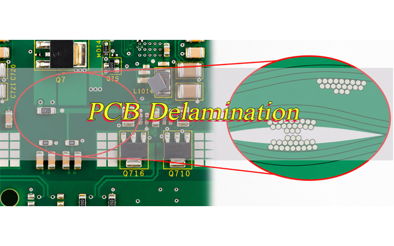
PCB delamination happens when bonded layers inside a PCB separate because of moisture, heat, weak adhesion, material stress, or process defects. It may appear as a blister, white area, lifted laminate, edge gap, or hidden internal separation found only after cross-section analysis.
The key issue is not only whether the defect is visible. A reliable judgment should confirm the PCB delamination root cause, check whether the board is still safe to use, and stop the same issue from entering SMT assembly or batch production.
What Is PCB Delamination?
PCB delamination is the separation of bonded layers inside a printed circuit board. It means the laminate, copper foil, prepreg, core, or solder mask has lost adhesion from the surrounding structure. This can happen between copper and dielectric, between prepreg and core, around plated holes, or near board edges.
Delamination of PCB materials may appear during fabrication, reflow soldering, rework, thermal cycling, or long-term field use. It is more serious than a surface mark because the separated area can grow under heat, humidity, vibration, or electrical stress.
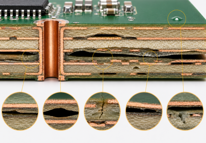
Common signs include blistering, raised laminate, white patches, edge lifting, and internal gaps. Some defects are visible on the surface, while others need cross-section inspection to confirm the real condition.
What Does PCB Delamination Cross Section Look Like?
PCB delamination cross section usually shows a gap, crack, void, or lifted interface inside the board. The clearest sign is a visible separation line between layers that should remain fully bonded. This may appear near copper foil, prepreg, glass fiber, plated through holes, or resin-rich areas.
In PCB delamination images, surface defects may look like bubbles, white patches, or pale marks. However, a cross section shows whether the defect is only near the surface or already inside the laminate. Under magnification, resin cracking, copper separation, air pockets, or fractured dielectric material may appear.
This inspection is important because a board can look acceptable from the outside but still contain hidden internal separation. Cross-section evidence helps confirm defect location, severity, and likely root cause.
What Causes PCB Delamination?
PCB delamination is usually caused by moisture, excessive heat, weak bonding, material mismatch, contamination, or poor lamination control. Most PCB delamination failures are not caused by one single factor. They often happen when material, storage, fabrication, and soldering risks combine.
Common causes include:
- Moisture absorption
PCB laminate can absorb moisture during storage, handling, or long air exposure. During reflow soldering, trapped moisture turns into vapor and creates internal pressure. If the pressure is stronger than the laminate bonding strength, blisters, bubbles, or internal separation may appear. - Excessive soldering temperature
Lead-free reflow, wave soldering, and hot-air rework expose the PCB to high heat. If the material cannot tolerate the peak temperature or repeated thermal cycles, resin stress increases and layer separation may occur. - Low Tg or low Td material
Tg affects dimensional stability under heat, while Td relates to resin decomposition. If the material has poor thermal resistance, the PCB becomes more vulnerable to delamination during assembly or long-term operation. - High Z-axis expansion
When the board is heated, the laminate expands through its thickness. High Z-axis CTE can create stress around plated holes, inner layers, and copper interfaces, especially in thick, multilayer, or heavy copper PCB structures. - Poor lamination control
Incorrect lamination temperature, pressure, vacuum, or resin flow can create weak bonding between prepreg, core, and copper layers. Resin starvation, trapped air, and incomplete curing can later develop into a PCB delamination issue. - Contaminated copper or laminate surface
Oil, oxidation, dust, chemical residue, or poor surface treatment can reduce bonding strength. Even if the PCB looks normal after fabrication, weak adhesion may fail during soldering heat or reliability testing. - Drilling, desmear, or plating stress
Rough drilling, over-aggressive desmear, or uneven plating can damage the hole wall and nearby laminate. These defects are more likely to cause separation around plated through holes after thermal stress. - Excessive rework or repeated heating
Repeated soldering and local hot-air repair can overheat the same area. This weakens resin, increases internal stress, and may turn a small hidden defect into visible PCB delamination.
In short, PCB delamination root cause analysis should check material selection, moisture control, lamination quality, surface cleanliness, drilling quality, and soldering profile together. Only checking the visible blister is not enough.
What Is the Problem With PCB Delamination?
The main problem with PCB delamination is that it damages the mechanical, electrical, and thermal reliability of the board. A small separated area can become a larger failure after reflow, rework, humidity exposure, or long-term operation. The risk depends on defect location and product application.
When layers separate, the dielectric structure changes. This may affect impedance, insulation resistance, heat transfer, and high-voltage spacing. Moisture may also enter the separated area and increase the risk of corrosion, leakage current, conductive anodic filament growth, or intermittent failure.
The most difficult part is timing. A PCB delamination issue may not appear during bare-board electrical testing. It may appear after SMT assembly, after functional testing, or after the product has already entered actual use.
How Bad Is Delaminating a PCB?
A delaminating PCB should not be used without evaluation. The real risk depends on where the delamination appears, how large it is, and whether it affects electrical, mechanical, or thermal performance. A board may still power on during a short test, but the separated area can grow under heat, humidity, vibration, or repeated operation.
Main risks include:
- Reduced electrical reliability
If delamination occurs near traces, vias, plated holes, or high-voltage spacing, it may affect insulation resistance, signal stability, or long-term electrical safety. Hidden separation may also lead to intermittent opens or leakage current. - Higher risk during soldering and rework
A delaminated area can expand during reflow, wave soldering, or hot-air repair. Trapped moisture and thermal expansion may turn a small blister into a larger PCB delamination issue after additional heating. - Weak mechanical strength
Delamination reduces the bonding strength between PCB layers. This is risky for connector areas, screw holes, edge plating areas, press-fit zones, and boards exposed to vibration or mechanical load. - Poor heat dissipation
Air gaps inside the laminate reduce heat transfer. In power electronics, LED products, charging modules, or high-current PCB designs, this may create local hot spots and shorten product life. - Signal or impedance problems
In RF, high-speed, or controlled impedance PCB designs, layer separation can change dielectric spacing. This may affect impedance control, signal loss, crosstalk, or high-frequency performance. - Moisture and corrosion risk
Once layers separate, moisture can enter the internal gap more easily. This may increase corrosion, copper migration, conductive anodic filament risk, and long-term field failure. - Possible batch quality problem
If the same defect appears on multiple boards, it may indicate a material, storage, lamination, or soldering process problem. In this case, the whole lot should be reviewed, not only the visible defective board.
In short, a small non-functional surface blister may be reviewed, but delamination near vias, pads, traces, BGA areas, high-voltage spacing, or thermal stress zones should be treated as high risk. For reliable production, cross-section analysis and root cause confirmation are safer than judging by appearance only.
How Do Tg, Td, CTE and Soldering Temperature Affect PCB Delamination?
Tg, Td, CTE, and soldering temperature directly affect PCB delamination risk. PCB delamination temperature is not a fixed value. It depends on laminate type, moisture content, board thickness, copper weight, layer count, and the full soldering profile.
Tg is the glass transition temperature. When a PCB is heated above Tg, the laminate expands faster and becomes less stable. If the board also has high moisture content or weak bonding, this expansion can increase internal stress and lead to layer separation.
Td is the decomposition temperature of the resin system. If the PCB material is exposed to excessive heat for too long, the resin may start to break down. Once the resin structure is damaged, the bonding strength between copper, prepreg, and core materials becomes weaker.
CTE shows how much the material expands when heated. The Z-axis CTE is especially important because PCB layers expand through the board thickness during reflow. High Z-axis expansion can stress plated holes, inner layers, and copper interfaces, increasing the chance of delamination.
Soldering temperature also matters. Lead-free reflow, wave soldering, and hot-air rework usually expose the PCB to higher heat than standard operating conditions. Multiple reflow cycles or repeated repair heating can make the problem worse, especially for thick PCB, multilayer PCB, heavy copper PCB, and boards stored in humid conditions.
In short, PCB delamination risk increases when low thermal resistance, high moisture absorption, high Z-axis expansion, and aggressive soldering heat appear together. For reliable production, the laminate should match the reflow profile, product temperature range, board structure, and expected rework conditions.
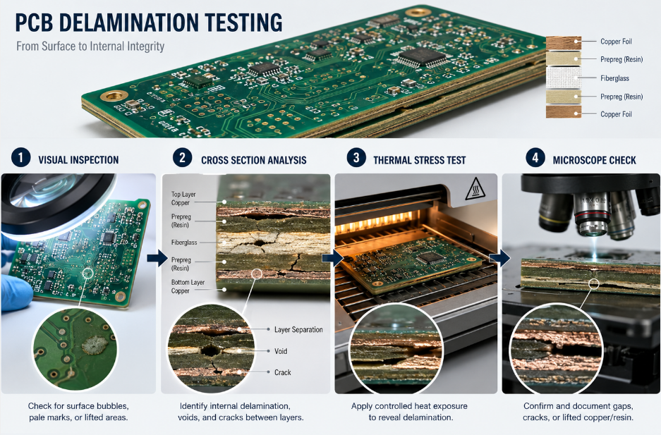
How to Test for PCB Delamination?
PCB delamination test should follow a clear inspection path from surface review to internal confirmation. The goal is not only to find the defect, but also to confirm its location, severity, and root cause. A visible blister may be only a surface symptom, while hidden separation may require thermal testing or cross-section analysis.
Step 1: Start with visual inspection. Check the PCB surface, edges, plated holes, solder mask areas, BGA areas, connector areas, and large copper zones. Look for blisters, raised laminate, white patches, edge lifting, discoloration, solder mask bubbling, or cracks around holes. This step helps define where further testing should focus.
Step 2: Review the defect location and risk level. Delamination near vias, pads, traces, controlled impedance layers, high-voltage spacing, or thermal stress areas should be treated as high risk. If the defect is only in a non-functional edge area, it may still need review, but the risk may be lower.
Step 3: Use thermal stress or reflow simulation when heat is suspected. The PCB can be exposed to a controlled soldering or thermal stress condition based on the actual assembly profile. If moisture, weak bonding, or poor material resistance exists, the defect may expand after heating.
Step 4: Use non-destructive inspection when hidden separation is suspected. Acoustic microscopy can help detect internal voids, gaps, or layer separation without cutting the board. This is useful when the surface looks normal but the product has reliability concerns after reflow or thermal cycling.
Step 5: Confirm the defect with cross-section analysis. The sample is cut from the suspected area, mounted, ground, polished, and inspected under magnification. Cross-section analysis can show whether the separation is at the copper-prepreg interface, inside the resin, around plated holes, or between laminate layers.
Step 6: Combine test results with process history. Material type, storage condition, baking record, lamination process, soldering profile, rework history, and defect position should be reviewed together. A reliable PCB delamination test should end with a root cause judgment, not only a pass/fail result.
How Does Cross-Section Analysis Identify PCB Delamination?
Cross-section analysis identifies PCB delamination by exposing the internal structure and showing exactly where the layers separated. It turns a surface symptom into physical evidence. This makes it one of the most useful methods for root cause analysis.
The process begins by selecting the defect area. The sample is usually taken from a blister, edge separation, plated hole, BGA area, connector area, or high-stress location. The sample is then cut, mounted in resin, ground, polished, and inspected under a microscope.
If separation appears at the copper-prepreg interface, weak bonding or surface treatment may be suspected. If resin voids appear inside prepreg, lamination or moisture may be involved. If cracks appear near plated holes, drilling, plating, or Z-axis expansion may be the cause.
How Can PCB Delamination Be Prevented?
PCB delamination can be prevented by controlling material, moisture, lamination, soldering heat, storage, and inspection. The best prevention method is to reduce bonding stress before the PCB reaches assembly or batch production.
- Choose the right laminate material
Select high-Tg, high-Td, low-CTE materials for lead-free reflow, high-temperature products, thick boards, multilayer PCB, heavy copper PCB, and power electronics. The material should match the soldering temperature, operating environment, and reliability requirement. - Control PCB moisture before assembly
Keep PCB boards in sealed dry packaging before SMT assembly. Long air exposure, damaged vacuum bags, high humidity, or poor storage conditions can increase moisture absorption and raise PCB delamination risk during reflow. - Use baking carefully when needed
Baking can help reduce absorbed moisture, but it should not be used blindly. Temperature and time should follow material type, surface finish, board thickness, storage history, and assembly requirements. Over-baking may affect solderability or surface finish quality. - Improve lamination quality
Lamination pressure, temperature, vacuum, prepreg condition, resin flow, and curing control must be stable. Poor lamination can create voids, weak bonding, resin starvation, or trapped air, which may later become delamination during soldering heat. - Keep copper and laminate surfaces clean
Contamination, oxidation, chemical residue, oil, or dust can reduce bonding strength. Proper surface treatment and clean process control help improve adhesion between copper, prepreg, core, and solder mask layers. - Avoid excessive thermal shock
Reflow profile, wave soldering temperature, and hot-air rework should be controlled. Multiple reflow cycles and repeated local heating can weaken resin and expand hidden separation, especially in thick or moisture-sensitive PCB structures. - Review design and stackup before fabrication
Balanced copper distribution, suitable material pairing, proper via design, and reasonable layer structure reduce internal stress. Thick copper, HDI, rigid-flex, and high-layer-count PCB projects should receive stronger DFM review. - Add inspection for high-risk projects
For high-reliability or first-batch production, add cross-section inspection, thermal stress testing, and material record review. Early inspection is more effective than discovering PCB delamination after SMT assembly or field use.
How to Fix a Delaminated Board?
A delaminated board usually cannot be restored to original reliability. Internal PCB delamination is normally not a true repair item; it is a reliability judgment and root cause issue. If internal layers, plated holes, impedance areas, high-voltage spacing, or solder pads are affected, replacement is safer than repair.
Minor surface lifting or solder mask issues may sometimes be reviewed for non-critical prototypes, but internal laminate separation is different. Resin cracks, copper separation, and internal air gaps cannot be reliably rebonded without changing the board structure.
Before any reuse decision, the board should pass visual review, electrical testing, thermal exposure review, and acceptance criteria. For production products, the better action is to isolate the lot, confirm the PCB delamination root cause, correct the process, and remake boards when reliability is at risk.
PCB Delamination Case Study: From Visual Defect to Root Cause Analysis
In one 6-layer FR-4 PCB project, raised circular areas appeared after lead-free reflow. The boards passed bare-board electrical testing before assembly, but some units failed functional testing after connectors were soldered. The visible defect looked like a local blister near a large copper area.
Cross-section analysis showed separation at the copper-prepreg interface and small voids in nearby resin-rich zones. The root cause was linked to absorbed moisture, insufficient storage control before assembly, and high thermal stress during reflow.
Corrective actions included dry storage control, reviewed baking conditions, adjusted reflow profile, tighter incoming inspection, and additional cross-section checks for the next pilot lot. After these changes, the PCB delamination issue was controlled before batch production.
FAQs About Delamination of PCB
Q1: Is delamination a defect?
A1: Yes. Delamination is a PCB defect because bonded layers have separated from each other. Even if the board still works, the separated area may grow during soldering, rework, thermal cycling, or humidity exposure. The final judgment should follow IPC class, project drawing, defect location, and product reliability requirements.
Q2: How much does it cost to fix delamination?
A2: The cost depends on whether the issue appears on a prototype, bare PCB, assembled PCBA, or production batch. Internal delamination is usually not cost-effective to repair for production use. Real cost may include inspection, cross-section analysis, scrap boards, lost components, remake, schedule delay, and quality risk.
Q3: Can a PCB pass electrical testing with delamination?
A3: Yes. A PCB can pass open and short testing while still having hidden laminate separation. Electrical testing checks connectivity at that moment, but it may not reveal weak adhesion or internal voids. This is why thermal stress, acoustic inspection, or cross-section analysis may be required for high-reliability boards.
Q4: Can X-ray find PCB delamination?
A4: X-ray may help find some internal defects, but it is not always the best method for laminate separation. Delamination can be thin and difficult to identify between similar materials. Acoustic microscopy and cross-section inspection are usually more useful when the goal is to confirm internal separation.
Q5: Does conformal coating stop delamination?
A5: No. Conformal coating protects the surface but does not rebond separated laminate layers. It may reduce moisture exposure after assembly, but it cannot fix internal voids, copper-prepreg separation, or resin cracks. If delamination already exists, the board should be evaluated before coating.
Q6: Why does delamination appear after reflow soldering?
A6: Reflow heats the PCB quickly. If moisture is trapped inside the laminate, it turns into vapor and creates internal pressure. When this pressure is stronger than layer bonding strength, blisters or separation appear. High peak temperature, fast ramp rate, repeated reflow, and poor storage can make the problem worse.
Q7: Is a small blister always a reason to scrap the board?
A7: Not always. A small blister in a non-functional area may be reviewed by location, size, and product class. However, blisters near vias, BGA pads, high-voltage spacing, controlled impedance traces, or solder joints are high risk. For production boards, cross-section analysis is often the safest judgment method.
Q8: Which PCB materials reduce delamination risk?
A8: Materials with higher Tg, higher Td, lower Z-axis CTE, lower moisture absorption, and stable resin systems reduce risk. High-Tg FR-4, polyimide, and special high-temperature laminates may be selected based on application. The best material should match reflow profile, operating heat, board thickness, and reliability class.
Q9: Can poor PCB design increase delamination risk?
A9: Yes. Unbalanced copper, large solid copper areas, weak stackup symmetry, poor via design, and local hot spots can increase stress. Design may not be the only cause, but it can make material and process risks worse. DFM review before fabrication helps reduce delamination risk.
Q10: What should be confirmed before ordering PCB production?
A10: Key items include material Tg/Td, IPC class, lamination control, storage method, reflow compatibility, cross-section capability, and defect handling process. For high-reliability projects, stackup confirmation, material data, inspection reports, and pilot-run test results should be reviewed before batch production.
Q11: Is delamination more common in multilayer PCB boards?
A11: Multilayer PCB boards can carry higher risk because more layers, more prepreg interfaces, thicker stackups, and stronger Z-axis stress create more bonding challenges. This does not mean multilayer boards are unreliable. It means material selection, lamination control, moisture management, and inspection must be stronger.
Q12: Can delamination happen before SMT assembly?
A12: Yes. Delamination can happen during lamination, drilling, desmear, plating, routing, solder mask curing, or thermal testing. Assembly may only expose an existing weakness. Sometimes the board looks acceptable before reflow, but heat makes the hidden defect visible.
Q13: Does board thickness affect delamination risk?
A13: Yes. Thicker PCB boards can retain more moisture and experience stronger Z-axis stress during heating. High layer count, heavy copper, buried vias, and mixed dielectric materials can also raise process difficulty. These projects need stronger material matching, dry storage, lamination control, and inspection.
Q14: What documents help prevent delamination disputes?
A14: Useful documents include fabrication drawing, IPC class, material data sheet, stackup, reflow profile, inspection plan, and acceptance criteria. Clear documents help judge whether a condition is acceptable, repairable, or rejectable. They also reduce disputes after production or assembly.
Q15: When should cross-section reports be requested?
A15: Cross-section reports are useful for high-layer-count PCB, HDI PCB, thick copper PCB, rigid-flex PCB, automotive PCB, medical PCB, power electronics, and first batch production. A cross-section report helps verify plating quality, internal bonding, layer structure, and hidden defects before mass production.
PCB delamination is not only a visible surface defect. It is a warning that material selection, moisture control, lamination, soldering temperature, storage, or quality inspection may not match the product requirement. The best technical approach is to confirm the separation location, identify the root cause, and prevent recurrence before batch production.
For material selection, focus on Tg, Td, CTE, soldering temperature, board thickness, copper weight, and real operating conditions. For PCB and PCBA projects, choose a China source factory that can support DFM review, material matching, lamination control, cross-section inspection, PCBA process feedback, and global delivery. Send your Gerber files, stackup, drawings, and assembly requirements to EBest Circuit for a fast quotation: sales@bestpcbs.com.