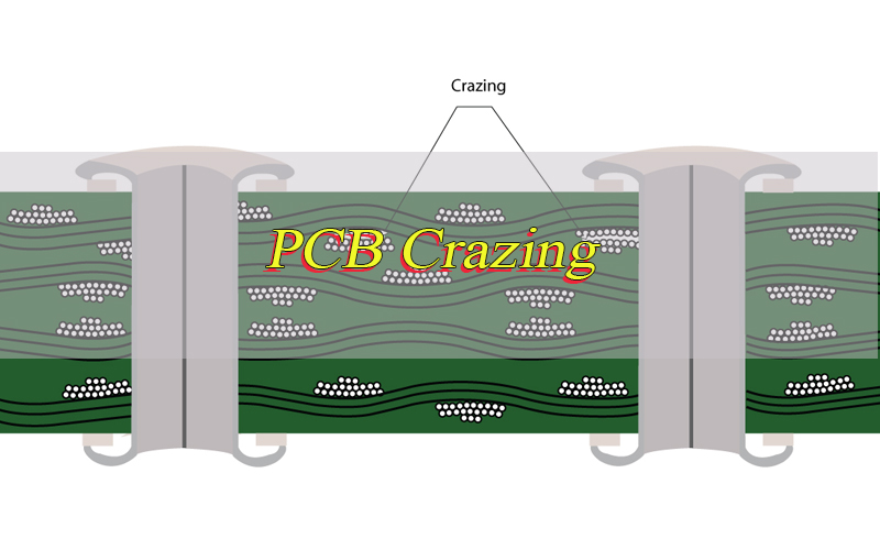
PCB crazing is a laminate defect that appears as fine white lines, cloudy marks, or glass-weave stress patterns inside a printed circuit board. It often points to resin-to-glass fiber separation caused by heat, moisture, drilling stress, bending, or unstable process control.
For most projects, the main concern is not only the appearance of the mark. The real question is whether the defect affects insulation, plated holes, copper adhesion, soldering reliability, or long-term field performance. This guide explains how to identify PCB crazing, inspect it before assembly, prevent repeat defects, and decide whether a crazed or cracked board can still be used.
What Is Crazing in PCB?
PCB crazing is an internal laminate defect where fine cracks or separations form between resin and glass fiber inside the PCB base material. It often looks like thin white lines, cloudy streaks, or connected stress marks under the board surface.
This defect is different from a simple solder mask scratch. A scratch usually stays on the surface, while crazing is related to the internal laminate structure. In PCB manufacturing, it may appear after drilling, routing, soldering, thermal shock, moisture expansion, or mechanical bending. When it appears near vias, plated through holes, high-voltage spacing, or fine traces, the reliability risk becomes much higher.
What Does PCB Crazing Look Like on a Printed Circuit Board?
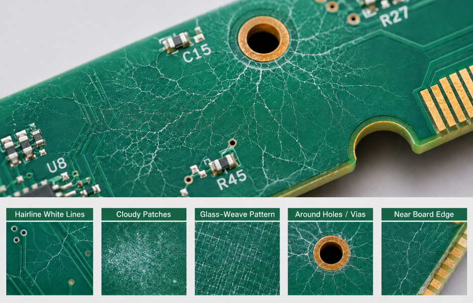
PCB crazing usually appears as white hairline marks, cloudy patches, or connected white lines following the glass fiber direction. It may be visible under normal light, but side lighting, backlighting, or magnification often makes the defect easier to identify.
Common visual signs include:
- White lines around drilled holes, slots, or board edges
- Web-like whitening inside the laminate
- Pale stress marks near copper areas
- Fine cracks following the glass weave
- Local whitening after reflow or wave soldering
- Marks close to vias, pads, or routed cutouts
However, visual appearance is only the first clue. The final judgment depends on defect depth, location, electrical spacing, product class, and actual test results.
Is PCB Crazing a Serious PCB Manufacturing Defect?
PCB crazing can be minor or serious depending on where it appears and how deep the laminate damage goes. A small isolated mark in a nonfunctional area may be acceptable after inspection, but a connected or deep defect near conductors should be treated carefully.
The risk is higher when the defect appears:
- Around plated through holes
- Between conductors with tight spacing
- Near high-voltage clearance areas
- Around heavy copper or high-current zones
- At board edges exposed to bending
- After reflow, wave soldering, or repair heating
- In automotive, medical, industrial, aerospace, or power electronics projects
For mass production, the safest rule is clear: do not assemble expensive components on a suspicious PCB before the laminate defect is confirmed.
What Causes PCB Crazing During PCB Manufacturing?
The main PCB crazing causes are moisture expansion, thermal shock, mechanical stress, weak lamination bonding, drilling damage, and unsuitable material selection. In real production, several causes may happen together.
Common causes include:
- Moisture absorption: Trapped moisture expands during soldering, baking, or hot air processes.
- Thermal shock: Fast heating during reflow, HASL, wave soldering, or rework stresses the resin system.
- Poor lamination control: Incorrect pressure, resin flow, or curing weakens resin-to-glass bonding.
- Drilling stress: Dull drills, wrong feed rate, or high drilling heat can damage nearby laminate.
- Mechanical bending: Depaneling, connector insertion, fixture pressure, or handling can create internal stress.
- Material mismatch: Low Tg, high CTE, or weak resin systems may fail under repeated thermal cycles.
- Copper imbalance: Uneven copper distribution increases warpage and localized stress.
Because most causes are process-related, prevention should start with material control, fabrication settings, and assembly temperature review.
Where Does PCB Crazing Commonly Appear?
PCB crazing commonly appears in areas where thermal or mechanical stress is concentrated. These areas should receive extra attention during incoming quality control, production inspection, and failure analysis.
Typical locations include:
- Around drilled holes: Vias, plated through holes, tooling holes, and mounting holes can carry drilling stress.
- Near board edges: Routing, scoring, punching, or rough depaneling can create edge cracks.
- Around slots and cutouts: Sharp internal corners concentrate mechanical stress.
- Near copper planes: Heavy copper and uneven copper balance can create expansion differences.
- Beside connectors: Press-fit parts, plug-in connectors, and repeated insertion can bend the board locally.
- After soldering areas: Reflow, wave soldering, selective soldering, and repair heating can reveal hidden moisture or weak bonding.
Location matters because the same visual defect may be acceptable in one area but unacceptable near electrical or mechanical stress points.
How Does PCB Crazing Affect PCB Reliability?
PCB crazing affects reliability by weakening laminate integrity and increasing the risk of moisture paths, insulation failure, copper separation, and crack growth. The risk depends on defect size, depth, location, and operating environment.
Possible reliability impacts include:
- Lower insulation resistance between nearby conductors
- Higher moisture penetration risk
- Weaker bonding between resin, glass fiber, and copper
- Crack growth during thermal cycling
- Reduced mechanical strength around holes and edges
- Higher failure risk under vibration or bending
- Possible conductive anodic filament risk in humid, high-voltage applications
For low-stress consumer products, a tiny isolated mark may not cause immediate failure. For power electronics, industrial controls, automotive modules, and medical devices, the acceptance threshold should be much stricter because field failure cost is far higher than bare board rejection cost.
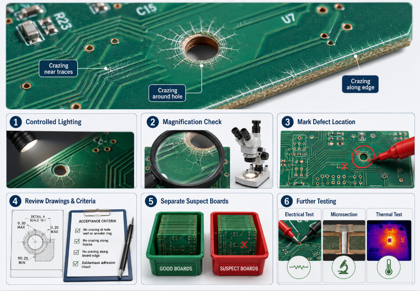
How to Inspect PCB Crazing Before PCB Assembly?
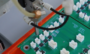
PCB crazing inspection should be completed before SMT assembly, especially when the mark appears near holes, traces, copper planes, connectors, or high-voltage spacing. The purpose is to prevent questionable bare boards from entering component mounting, soldering, and functional testing.
Step 1: Review the defect area under controlled lighting.
Place the board under bright, stable light and check it from different angles. Side lighting can reveal white lines, cloudy streaks, and stress marks that are not obvious under normal inspection. If the board is thin or translucent, backlighting may help expose whitening inside the laminate.
Step 2: Use magnification to confirm the defect shape.
Inspect the area with a magnifier or microscope. Check whether the mark is a surface scratch, solder mask damage, glass-weave whitening, or internal laminate stress. Pay special attention to hole edges, slot corners, routed edges, and dense via areas.
Step 3: Mark the defect location on the board map.
Record whether the mark is close to pads, traces, vias, plated through holes, copper planes, or clearance areas. A defect in a nonfunctional corner has a different risk level from a defect between conductors or beside a connector.
Step 4: Compare the board with drawings and acceptance criteria.
Review the fabrication drawing, PCB class, voltage spacing, customer notes, material requirement, and final application. Boards for industrial, automotive, medical, or high-voltage use should follow stricter judgment than simple low-risk commercial boards.
Step 5: Separate suspicious boards before assembly.
Affected boards should be held and clearly identified. Do not mix them with normal production lots, because once components are assembled, inspection becomes harder and repair cost increases.
Step 6: Decide whether further testing is required.
If the defect is close to functional copper, plated holes, or high-stress areas, visual inspection alone is not enough. Electrical testing, microsection analysis, or thermal stress testing should be used before the board enters assembly.
What Testing Methods Can Confirm PCB Crazing Defects?
PCB crazing defects can be confirmed by combining visual inspection, microsection analysis, electrical testing, and reliability testing. The right method depends on defect location, product risk, and whether the board is for prototype, pilot run, or mass production.
- Visual inspection:
This is the first screening method. It helps identify whitening, hairline marks, glass-weave stress, and abnormal areas around holes, edges, slots, and soldered zones. It is fast, but it cannot confirm defect depth. - Backlighting inspection:
Backlighting is useful for thin boards or translucent laminate areas. It can make internal white marks more visible and help distinguish surface contamination from internal stress marks. - Microscope inspection:
Magnification helps confirm whether the mark follows the glass fiber direction, starts from a drilled hole, or extends from a routed edge. It is useful for printed circuit board crazing inspection before assembly. - Microsection analysis:
Cross-section testing is the most direct method for confirming internal laminate damage. It shows whether the defect reaches glass fiber, resin-rich areas, plated holes, copper interfaces, or inner layers. - Continuity test:
This test checks whether traces or plated holes have open circuits. It is important when the defect is near vias, pads, or narrow conductors. - Insulation resistance test:
This test checks leakage risk between nearby conductors. It is especially useful for high-voltage boards, fine-pitch layouts, and products used in humid environments. - Thermal stress test:
Reflow simulation, solder float, or thermal cycling can reveal whether the defect expands after heat exposure. It helps judge whether the board can survive assembly and field operation. - Humidity-related reliability test:
Humidity testing helps evaluate moisture penetration and insulation stability. It is useful for outdoor electronics, power modules, industrial controls, and long-life products.
A practical confirmation plan should not rely on one method only. For high-reliability projects, visual evidence, electrical data, microsection results, and product application risk should be reviewed together.
How Can PCB Crazing Be Prevented in PCB Manufacturing?
PCB crazing prevention depends on moisture control, stable materials, proper lamination, controlled drilling, safe routing, balanced copper, and suitable soldering temperature. Prevention is more reliable than repair because internal laminate damage cannot be fully restored after it forms.
- Control material storage before production:
Laminates, prepregs, and finished boards should be stored in dry, sealed, and traceable conditions. Moisture absorption is one of the most common contributors to whitening, stress marks, and laminate damage during thermal processing. - Use proper baking when moisture risk exists:
Boards stored for a long time, exposed to humidity, or used in lead-free assembly may require controlled baking before soldering. Baking should be based on material type, board thickness, and customer requirements, not random high-temperature treatment. - Select laminate suitable for the application:
Low-cost material may work for simple electronics, but it may not be suitable for repeated reflow, high humidity, high voltage, or harsh field environments. Tg, Td, CTE, resin system, and moisture absorption should match the real use condition. - Stabilize lamination process control:
Incorrect temperature, pressure, resin flow, or curing can weaken bonding between glass fiber and resin. Stable lamination helps reduce internal stress and improves long-term board reliability. - Optimize drilling parameters:
Dull drill bits, excessive feed speed, poor chip removal, and high drilling heat can damage the laminate around holes. Tool life control, suitable drill speed, and clean hole wall preparation help reduce local stress. - Improve routing and depaneling support:
Rough routing, sharp slot corners, punching, or unsupported depaneling may create cracks at edges and cutouts. Smooth routing, radiused corners, proper fixture support, and controlled V-score depth reduce mechanical damage. - Balance copper distribution in the stack-up:
Large copper imbalance can increase warpage and expansion mismatch during heat exposure. Better copper symmetry and panel design help reduce internal stress during lamination and assembly. - Control soldering and rework temperature:
Excessive peak temperature, long dwell time, repeated rework, and uncontrolled hot air repair can expand small laminate weaknesses. A stable reflow profile and limited rework cycles help prevent defect growth.
For mass production, the best prevention method is not a single process change. It is a complete control plan covering material storage, DFM review, fabrication parameters, assembly profile, and final inspection.
What Design and Material Factors Can Reduce PCB Crazing Risk?
Design and material decisions can reduce PCB crazing risk before production starts. A reliable PCB should be designed around thermal stress, mechanical support, copper balance, board thickness, hole structure, and operating environment.
- Choose laminate with suitable Tg and Td:
High Tg material improves resistance to lead-free soldering and repeated heat exposure. Higher Td helps reduce decomposition risk when the board faces high-temperature processes or long operating life. - Review CTE for thermal expansion control:
A lower CTE helps reduce expansion mismatch between copper, resin, and glass fiber. This is important for multilayer boards, heavy copper boards, high-voltage boards, and products exposed to thermal cycling. - Avoid unnecessary thin board design:
Thin boards bend more easily during handling, connector insertion, depaneling, and assembly. If the product has large connectors, heavy components, or mechanical fixing points, board thickness should be reviewed carefully. - Balance copper across layers:
Uneven copper distribution creates stress during lamination and soldering. Large copper planes on one side and sparse copper on the other side can increase warpage and local laminate strain. - Use rounded corners for slots and cutouts:
Sharp internal corners are common crack-starting points. Rounded corners reduce stress concentration and help prevent edge-related laminate damage. - Keep enough spacing around holes and edges:
Dense vias, narrow webs, and holes too close to routed edges can weaken local structure. Enough spacing improves mechanical strength and reduces stress around drilled areas. - Match surface finish with assembly process:
ENIG, HASL, OSP, immersion silver, and other finishes have different thermal exposure and handling requirements. The finish should match solderability, storage time, assembly temperature, and product reliability level. - Consider the operating environment:
Outdoor, automotive, power, medical, and industrial PCBs may face humidity, vibration, temperature cycling, or high voltage. These projects should use stronger material and stricter inspection standards than simple consumer boards.
For customers, the key is to confirm material and design risks before placing a mass production order. A small DFM review before production can prevent larger lot rejection, assembly delay, and field failure later.
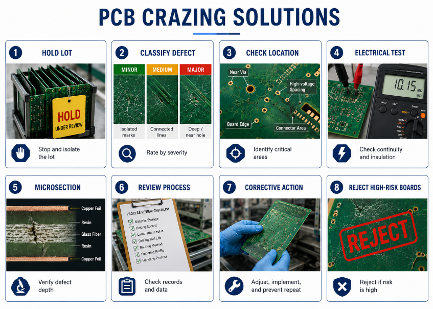
What PCB Crazing Solutions Can Be Used After Defects Are Found?
PCB crazing solutions should start with lot control, risk classification, and root cause analysis. Surface repair is not the first step because the defect may already exist inside the laminate.
- Hold the affected lot immediately:
Stop the lot from entering SMT assembly, shipment, or final product build. Mixing suspicious boards with normal boards makes traceability difficult and increases quality risk. - Classify the defect by severity:
Separate minor visual marks from internal laminate damage. Check whether the mark is isolated, connected, deep, or close to functional copper. - Check the location carefully:
Defects near plated holes, vias, conductor spacing, high-voltage areas, connectors, board edges, or mounting points should be treated as higher risk. Defects in nonfunctional areas may be reviewed with more flexibility. - Run electrical verification:
Continuity testing and insulation resistance testing should be used when the defect is close to traces or spacing. A board that passes visual inspection may still have hidden electrical risk. - Use microsection analysis for unclear defects:
If the defect depth is uncertain, cross-section testing can confirm whether the laminate, copper interface, hole wall, or inner layer is affected. - Review process history:
Check material storage, baking record, lamination profile, drilling tool life, routing method, soldering profile, and handling process. The goal is to find the real source, not only sort finished boards. - Apply corrective action before the next batch:
Adjust baking, drilling parameters, routing support, copper balance, lamination control, or material grade based on actual root cause. Repeat defects should not be accepted as normal production variation. - Reject boards with structural or electrical risk:
If the defect affects plated holes, insulation, copper adhesion, mechanical strength, or high-voltage clearance, replacement is safer than repair.
The right response depends on product risk. Prototype boards may allow limited engineering judgment, but mass production boards should follow agreed acceptance criteria and documented corrective action.
Can a Crazed or Cracked PCB Be Repaired?
A crazed PCB is usually not truly repairable because the damage is inside the laminate. Surface coating, epoxy, or cleaning cannot fully restore separated resin and glass fiber.
A cracked PCB may be repaired only when the damage is local and low-risk. For example, one broken trace on a prototype board may be restored with trace repair, jumper wire, reinforcement, or epoxy support. This type of repair is usually for temporary recovery, not long-term production use.
For automotive, medical, aerospace, industrial control, power electronics, or high-voltage products, replacement is safer. If the defect affects insulation, plated holes, copper adhesion, or mechanical strength, the board should not be used in mass production. The practical answer to “Can a cracked PCB be repaired?” is: sometimes for prototypes, rarely for reliable production.
| Condition | Repair Option | Production Decision |
|---|---|---|
| Minor surface mark | Review and test | May accept if criteria allow |
| Isolated nonfunctional area | Inspect and document | Conditional acceptance |
| Near PTH or via | Cross-section required | High caution |
| Near high-voltage spacing | Insulation test required | Usually reject |
| Broken trace | Local repair possible | Not for critical production |
| Structural crack | Reinforcement possible | Replace preferred |
| Internal crazing | Not fully repairable | Root cause control |
| Repeated lot defect | Process correction | Hold shipment |
FAQs About PCB Crazing
Q1: Is this laminate defect covered by IPC inspection standards?
A1: This issue is normally judged through visual acceptability, customer drawings, product class, and agreed inspection criteria. IPC-related inspection logic can help classify laminate defects, but the final decision should also consider board location, electrical spacing, product application, and reliability risk. For critical products, appearance alone is not enough.
Q2: Can this defect appear after the board passes factory inspection?
A2: Yes. Some defects may become visible after reflow, wave soldering, baking, connector insertion, or mechanical assembly. Heat and stress can expose hidden moisture or weak laminate bonding. This is why customers should review not only bare board inspection, but also assembly profile, storage time, and handling method.
Q3: Does board thickness affect this risk?
A3: Yes. Very thin boards bend more easily during handling, depaneling, fixture loading, and connector assembly. Thick boards may carry more thermal stress if copper balance and lamination are not controlled well. The right thickness should match mechanical support, component weight, assembly process, and final product structure.
Q4: Can this defect affect high-voltage products?
A4: Yes. High-voltage boards are more sensitive because laminate cracks may create moisture paths or reduce insulation stability between conductors. Even a small internal defect can become risky in humid or polluted environments. For high-voltage projects, insulation resistance testing and stricter spacing review are strongly recommended.
Q5: Should prototype boards with white laminate marks be used for testing?
A5: They can be used only after inspection and electrical verification. For simple power-on checks, a minor mark in a noncritical area may be acceptable. For thermal, vibration, high-voltage, or life-cycle tests, questionable boards should be avoided because they may distort test results and hide real design performance.
Q6: What information should customers send when reporting this issue?
A6: Customers should send clear photos, Gerber files, stack-up, material grade, board thickness, copper thickness, surface finish, quantity, lot number, soldering profile, and application environment. Complete information helps the supplier judge whether the defect is related to design stress, material choice, fabrication process, or assembly handling.
Q7: Can storage conditions cause similar laminate damage later?
A7: Poor storage can increase moisture absorption and make laminate defects more likely during soldering. Boards should be sealed, stored in dry conditions, and protected from long humidity exposure. For boards stored for a long time or exposed to high humidity, controlled baking may be required before assembly.
Q8: Is this issue more common near connectors?
A8: It can be. Connectors often create local stress during insertion, removal, screw fixing, press-fit assembly, or cable pulling. If the board is thin, poorly supported, or has copper imbalance around the connector area, the laminate may show stress marks. Stronger support and better layout spacing can reduce this risk.
Q9: Can conformal coating hide this problem?
A9: Conformal coating may cover the surface visually, but it does not repair internal laminate damage. If a board has real internal cracks, coating may only delay visible symptoms while the structural weakness remains. Before coating, the board should pass visual inspection, electrical testing, and risk review.
Q10: Does surface finish influence this risk?
A10: Surface finish is usually not the direct cause, but some finishes expose the board to more heat or handling during production. HASL, for example, involves thermal shock, while other finishes may require different storage and assembly controls. The finish should match soldering process, shelf life, and reliability requirements.
Q11: Can this defect cause intermittent failures?
A11: Yes. Intermittent failure may happen if the defect grows under vibration, bending, humidity, or temperature cycling. The board may pass a simple continuity test at room temperature but fail under real operating stress. For critical products, functional testing alone is not enough; reliability testing may be required.
Q12: How can buyers reduce this risk before ordering?
A12: Buyers should confirm material grade, Tg, board thickness, copper balance, soldering temperature, operating environment, and inspection requirements before ordering. Sending complete Gerber files and stack-up details allows the supplier to review risk early. Early DFM review is cheaper than rejecting assembled boards later.
Conclusion
PCB crazing is a laminate reliability warning that should be checked before assembly, not ignored as a simple white mark. The key judgment factors are defect location, depth, electrical spacing, plated hole condition, product class, and operating environment. For reliable products, prevention through material control, stable fabrication, proper inspection, and careful assembly is always better than repair.
EBest Circuit is a China source PCB and PCBA manufacturer providing custom PCB fabrication, assembly support, quality inspection, and global delivery for industrial, commercial, power, medical, and communication electronics projects. If your project requires reliable PCB manufacturing, defect prevention, or PCB crazing risk review, send your Gerber files, stack-up, material requirement, quantity, and application details to sales@bestpcbs.com for a quotation.