Pad Cratering is a fracture inside the PCB laminate beneath a copper pad, most often at BGA corners. The pad can remain attached to the solder ball while resin and glass separate from the board. Prevention depends on laminate selection, land design and control of board strain.
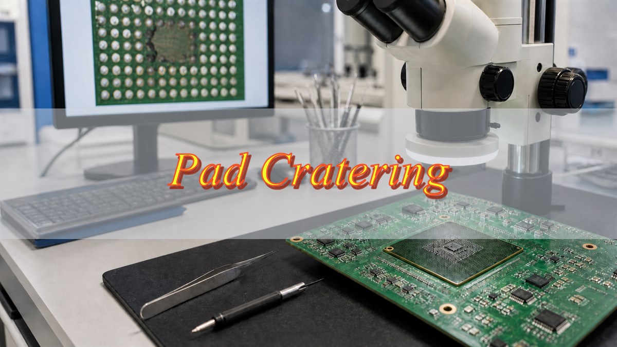
What Is Pad Cratering in PCB?
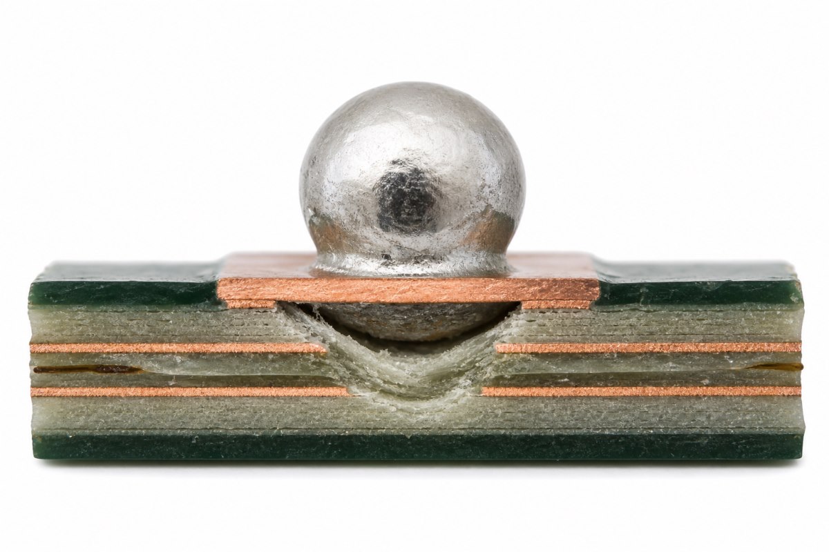
IPC-9708 describes pad cratering as a cohesive failure in the printed board laminate under a BGA pad. The copper land and solder joint may remain together while resin or resin-glass material tears away below them. Large, stiff area-array packages are vulnerable because board bending concentrates strain near their corners.
Standards note: IPC-9708, published in 2010, remains a useful test-method reference, but IPC’s document revision table currently marks it “No Longer Maintained.” Treat it as a characterization framework and agree acceptance criteria, specimen design and statistics with the customer or qualification authority.
What Does a PCB Pad Cratering Failure Look Like?
A confirmed crater usually appears as a shallow, irregular fracture in the laminate beneath the copper pad, with resin and sometimes glass fibers remaining on the separated land.
| Observation | What it may indicate | Best confirmation |
| Intermittent BGA connection after handling | Crater or trace crack opening only under board flex | Continuity monitoring during controlled flex, then cross-section |
| Pad remains attached to solder ball after separation | Pad crater or pad lift | Inspect the fracture surface and laminate beneath the pad |
| Resin/glass material on pad underside | Cohesive laminate fracture | Optical microscopy and polished cross-section |
| Corner joints affected first | Package/board bending concentration | Strain history, event reconstruction and sectioning |
| Visible copper trace break outside the pad | Trace fracture, possibly secondary to the same bend event | Electrical localization and cross-section |
- The copper pad may remain attached to the solder ball.
- Resin or glass fibers may remain on the pad underside.
- Corner joints are common locations.
- A normal X-ray does not rule out a thin laminate crack.
What Problems Can BGA Pad Cratering Cause in a PCB Assembly?
BGA pad cratering can create a permanent open circuit, an intermittent connection or a mechanically weakened joint that fails later in service.
- Intermittent operation: the cracked interface may make contact at rest and open during vibration, enclosure flex or temperature change.
- No-fault-found returns: removing the load can temporarily restore continuity, making bench diagnosis difficult.
- Latent reliability loss: a partial crater can grow during later shock, vibration or handling events.
- Collateral damage: the same board bend can crack a neck-down trace, solder joint or nearby component termination.
- Difficult rework: replacing the BGA does not repair fractured laminate or an internal connection beneath the land.
What Factors Increase the Risk of PCB Pad Cratering?
Risk rises when a weak laminate-pad system is combined with a stiff package and a high local board strain rate or amplitude.
| Risk group | Examples | Engineering implication |
| Laminate | Low fracture toughness, resin-rich region, glass weave/resin interface, thermal history | Compare representative constructions, not only nominal Tg |
| Package | Large body, high I/O count, stiff package, corner joint geometry | Corner lands often deserve focused testing and inspection |
| Land and trace | Pad diameter, solder-mask opening, escape trace direction, neck-down geometry | Small geometry changes can move the highest stress or the fracture path |
| Assembly | Depaneling, fixture support, press-fit insertion, connector mating, heatsink or screw installation | Measure strain at the actual high-risk process step |
| Product use | Drop, mechanical shock, enclosure bending, connector load | Board-level and product-level tests answer different questions |
| Thermal-mechanical | Reflow exposure, CTE mismatch, thermal cycling followed by mechanical load | Thermal history can alter the system before a mechanical event |
Lead-free reflow history, laminate choice and stiff SAC joints can change the failure balance, but not every lead-free BGA failure is pad cratering. Confirm the fracture plane.
How Do Board Flexure and Mechanical Shock Trigger Pad Cratering?
Board flexure creates out-of-plane deformation; the stiff BGA resists that curvature and concentrates tensile and peel stresses near its outermost solder joints.
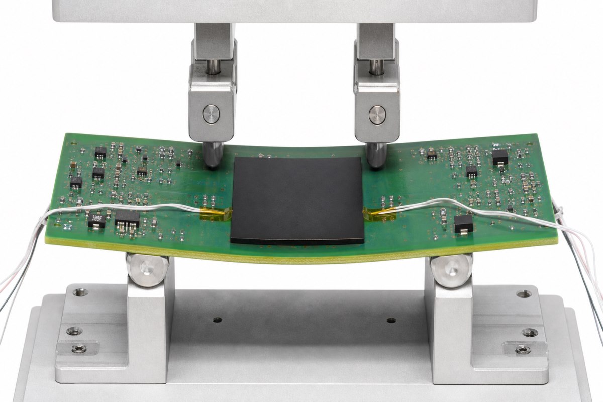
- Mechanical shock: short, high-rate board deflection.
- Depaneling or fastening: slower but localized bending.
- Key variables: strain amplitude, strain rate, support and curvature direction.
NASA’s lead-free electronics joint testing reported pad cratering among BGA failures after mechanical shock and noted corner solder joints as early failure locations in examined assemblies. That evidence supports corner-focused analysis, but it does not provide a universal allowable strain for every stackup and package.
How Can You Confirm Pad Cratering After a BGA Failure?
Confirmation requires locating the suspect net and then showing that the fracture lies in the PCB laminate below the pad.
- Preserve the evidence. Record handling, drop, depaneling, connector and screw-installation history before rework changes the fracture.
- Localize electrically. Use continuity, boundary scan or functional diagnostics; monitor the net during carefully controlled flex only when the risk is understood.
- Screen nondestructively. X-ray can identify competing solder defects. Acoustic emission can detect fracture events during controlled mechanical testing, but it does not by itself identify the final fracture plane.
- Expose the interface. Dye-and-pry can map separated interfaces across an array, although interpretation depends on dye penetration and the destructive separation procedure.
- Cross-section the target. A polished microsection through the pad, solder joint and adjacent trace is the strongest visual confirmation of a cohesive laminate crack.
- Classify mixed damage. Document whether pad cratering, solder fracture and trace cracking coexist and avoid assigning the first event from a final section alone unless evidence supports the sequence.
A useful failure-analysis report should separate observation from interpretation. Include the suspect net, package corner, fracture-plane photographs, cross-section orientation, event history and competing damage. If the sequence cannot be proven, state that limitation instead of presenting mixed damage as a single-cause conclusion.
What Pad Cratering Test Methods Are Used to Evaluate PCB Reliability?
Common evaluation methods either load an isolated land to compare material strength or bend/shock a populated assembly to reproduce system-level stress.
| Method | Primary output | Best use | Main caution |
| Pin-pull | Peak force and failure mode | Direct comparison of pad/laminate constructions | Pin attachment and coupon preparation affect results |
| Cold-ball pull | Pull force and fracture classification | Testing a solder ball/land system | Solder and ball attachment add variables |
| Ball shear | Shear force and failure mode | Fast comparative screening | Tool height, speed and solder response influence the result |
| Spherical/board bend | Load, displacement, strain or cycles to failure | Board-level interconnect behavior | Fixture and component layout must represent the question |
| Mechanical shock/drop | Electrical events and physical failure | Product or assembly dynamic robustness | Final damage may include several competing failure modes |
| Strain-gage process study | Local strain and strain rate | Depaneling, insertion, fastening and handling control | It measures exposure, not laminate strength directly |
IPC-9708 covers pin-pull, cold-ball-pull and shear methods. Qualification plans should cite the exact document revision, specimen geometry and agreed deviations.
How Is Pad Cratering Strength Measured with a Pad Pull Test?
A pad pull test applies a controlled tensile load normal to the land and records the peak force together with the observed failure mode.
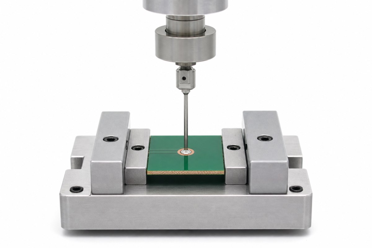
- Attach and align the pull pin to a defined test pad.
- Pull at the specified rate and record force-displacement data.
- Classify every fracture: laminate crater, pad separation, solder failure or invalid attachment failure.
- Report sample size, distribution and failure modes—not one maximum value.
Pull force is not a universal material property. Pad geometry, solder mask, trace connection, laminate, reflow history, rate and alignment all affect the result.
For material comparisons, lock the coupon drawing, copper treatment, conditioning, pull rate and failure taxonomy before testing. Compare valid crater failures under the same conditions. A higher average force is not persuasive if specimens fail at the pin attachment or use a different pad geometry.
Pad Cratering vs Pad Lift vs Trace Fracture: What Is the Difference?
The three failures are separated by where the crack travels: through laminate, along the pad interface or through copper trace.
| Failure mode | Fracture location | Typical evidence | Repair implication |
| Pad cratering | Within resin or resin-glass laminate below/around land | Laminate material attached to pad; subsurface cavity | BGA replacement alone may not restore board integrity |
| Pad lift | At copper-to-dielectric interface, often with land peeled away | Relatively clean interface or visibly raised land | Land repair may be possible only under controlled criteria |
| Trace fracture | Through copper conductor, often at pad neck-down | Open copper trace with laminate largely intact | Requires conductor repair or board replacement |
| Solder-joint fracture | Within solder or at an intermetallic interface | Fracture surface confined to joint system | Rework may restore connection if the PCB pad is sound |
One overload can produce mixed damage, so document every observed fracture plane.
How to Select PCB Materials and BGA Pad Design to Reduce Pad Cratering
Select materials and land structures by comparative mechanical evidence from the intended stackup, thermal history and package geometry—not by Tg alone.
- Ask for laminate-specific evidence. Compare representative resin systems and glass styles using a controlled pad-cratering method after the planned reflow exposures.
- Review toughness, not only heat resistance. Tg, Td and z-axis CTE describe important thermal behavior but do not directly state cohesive pad-cratering strength.
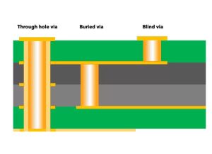
- Control construction details. The choice of PCB laminate, resin and glass fiber, copper treatment and the local dielectric configuration beneath critical lands can affect crack initiation.
- Avoid abrupt stress raisers. Review escape-trace neck-downs, sharp geometry transitions and the direction of traces at package corners.
- Follow the component supplier’s land pattern. Package-specific recommendations should be the starting point; deviations need assembly and reliability validation.
- Test the full design. A pad coupon ranks a laminate/land system, while bend and product shock tests evaluate the assembled structure.
Call a laminate “pad-cratering resistant” only when it performs better in an agreed comparative test for the target design.
Do SMD Pads and Underfill Help Reduce Pad Cratering?
Solder-mask-defined (SMD) pads and underfill can redistribute load, but either change may move stress to another location and must be validated at assembly level.
- SMD pads: solder-mask overlap can improve pad retention but adds a mask-edge stress concentration.
- NSMD pads: provide different routing and joint geometry; follow the package supplier’s land pattern.
- Underfill: can reduce joint motion during shock, but modulus, cure, fillet shape and rework needs matter.
- Validation: a stiff underfill may move stress into the laminate or nearby structures.
How to Reduce Pad Cratering During PCB Assembly and Manufacturing
The most effective manufacturing controls reduce board strain during PCB assembly and testing, especially at process steps that bend the board after BGA attachment.
- Map high-risk operations. Include depaneling, connector insertion, ICT/functional fixtures, shield or heatsink installation, screw tightening and manual handling.
- Measure local strain. Place strain gauges near critical package corners and capture peak strain, strain rate and bending direction under repeatable conditions.
- Support close to the load. Adjust fixtures, anvils and tooling so force does not travel through an unsupported board span.
- Replace uncontrolled separation. Use appropriate routed panels, scored-panel tooling or controlled depaneling equipment instead of hand flexing.
- Control insertion and fastening. Align connectors, use hard stops where suitable and manage screw sequence and torque to limit local curvature.
- Protect during transport. Use carriers and packaging that prevent populated boards from acting as flexible levers.
- Validate changes physically. Repeat representative strain measurements and reliability tests after stackup, package, fixture or enclosure changes.
Set process controls from measured evidence. A strain limit from another product is only a starting point because board thickness, package size, layout and support conditions change the response. Establish the baseline on the actual assembly and repeat the measurement after fixture or process changes.
FAQs About PCB Pad Cratering
Q1: What information should be shared before a pad cratering risk review?
A1: Share the PCB stackup, laminate and glass style, BGA part number, land pattern, reflow profile, panel format and expected mechanical loads. Add enclosure drawings and assembly steps when screws, connectors or depaneling can bend the board.
Q2: When should strain gauges be used during assembly qualification?
A2: Use them for depaneling, connector insertion, fixture clamping, screw tightening or heatsink installation. Measure near high-risk package corners on the actual product rather than relying only on a generic limit.
Q3: Can an ICT or functional-test fixture increase failure risk?
A3: Yes. Poor support or excessive clamp travel can flex the board repeatedly. Check support-pin location, clamp force, probe load and package clearance, then measure the worst production cycle.
Q4: How many samples are needed for a comparative pad-strength study?
A4: There is no universal count. Use enough valid specimens to show the force distribution and failure-mode population, and document excluded attachment failures. Customer or qualification requirements may set the final number.
Q5: Does PCB surface finish determine resistance to this failure?
A5: Surface finish affects solderability and joint interfaces, but the crater forms in the laminate. Treat finish as one system variable; ENIG, ENEPIG or OSP alone does not prove laminate fracture resistance.
Q6: Can moisture exposure change the risk?
A6: Moisture and thermal conditioning can change resin behavior and reflow response. Use controlled storage, representative preconditioning and the same reflow history when comparing constructions.
Q7: What evidence should appear in a supplier failure-analysis report?
A7: Look for fracture-plane images, cross-section orientation, affected net and package location, event history, competing failure modes and an evidence-based conclusion. A photograph without specimen location or test conditions is not enough.
Q8: When is underfill worth evaluating?
A8: Consider it when shock or board flex cannot be reduced adequately by layout, support or process changes. Validate modulus, cure, temperature range, rework impact and the new failure location on the complete assembly.
Q9: Can a small layout change invalidate earlier reliability results?
A9: It can. Changes to board thickness, copper balance, package location, trace escape, cutouts, mounting holes or support points may alter local curvature. Repeat targeted tests when the mechanical response changes.
Q10: What should buyers ask before accepting a “pad-cratering-resistant” laminate claim?
A10: Ask for the exact construction, coupon drawing, reflow conditioning, test method, test rate, sample count, statistical results and classified fracture modes. Confirm that the tested construction matches the production stackup.
Final Engineering Checklist
Pad Cratering prevention works best as a closed loop: select and compare the laminate/land system, measure assembly strain, reproduce product loads, classify the actual fracture plane and feed the result back into material, layout and tooling decisions.
- Define the exact package, stackup, land pattern and thermal history.
- Agree the characterization method, specimen geometry and acceptance statistics.
- Monitor board strain during high-risk manufacturing operations.
- Confirm failures by cross-section or another validated physical method.
- Requalify material, design, fixture and enclosure changes that alter load paths.
Reduce BGA reliability risk before it reaches production. Send your stackup, BGA package details, land pattern and expected mechanical loads to sales@bestpcbs.com. Our engineering team can review the manufacturing risks and prepare a focused PCB/PCBA quotation for prototypes or volume production.