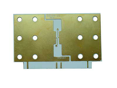
Thick Film Ceramic PCB Technical FAQ’s
1. What is the standard thickness of a thick-film ceramic board? +
0.635mm
2. What is the maximum size of thick film ceramic PCB? +
114mm x 114mm
3. What is the commonly referred name for the solder mask used on thick film ceramic PCB? What colors are available? +
It is called glass glaze, and the available colors are greenish-blue/blue.
4. What is the surface treatment for thick film ceramic PCB? +
No additional surface treatment is required.
5. How many types of substrates are typically used for thick film ceramic PCB? What are they? +
There are 3 types: Alumina, Aluminum Nitride, and Beryllium Oxide.
6. What are the color differences between the three substrates used in thick film ceramic PCB? +
Alumina and Beryllium Oxide are white, while Aluminum Nitride is gray.
7. How many types of Alumina substrates are there? +
96% Al₂O₃ and 99% Al₂O₃.
8. How are Alumina, Aluminum Nitride, and Beryllium Oxide written in English? +
Alumina: Aluminium Oxide/Alumina; Aluminum Nitride: Aluminium Nitride; Beryllium Oxide: Beryllium Oxide.
9. What are the dielectric constants of Alumina, Aluminum Nitride, and Beryllium Oxide? +
96% Al₂O₃: 8.9; 99% Al₂O₃: 9.5; AlN: 8.9; BeO: 6.4.
10. What conductor pastes are commonly used for thick film ceramic PCB? +
AgPd and Au.
11. What are the typical thicknesses of the conductor pastes for thick film ceramic PCB? +
AgPd: ≥10µm, Au: 3-7µm.
12. Can copper be used as a conductor on thick film ceramic PCB? +
No.
13. Are the circuits on thick film ceramic PCB created using printing or etching processes? +
They are created using a printing process.
14. How are the conductor paste and ceramic material bonded together? +
Through high-temperature sintering.
15. What is the peak sintering temperature for the conductor on thick film ceramic PCB? +
850°C ± 10°C.
16. What is the dwell time at peak temperature? +
8 minutes to 10 minutes.
17. What is the sintering cycle time? +
30 minutes to 60 minutes.
18. What is the operating temperature of thick film ceramic PCB? +
-55°C to 850°C.
19. Do thick film ceramic PCB require an insulating material between the conductor and substrate? +
No, ceramic materials are inherently insulating.
20. Can thick film ceramic PCB be screen-printed? +
Yes, but it is generally not done as it is quite complex to manufacture.
21. What is the minimum line width and spacing for thick film ceramic PCB? +
For samples: 0.2/0.2mm, for mass production: ≥0.25/0.25mm.
22. Can resistors be sintered on thick film ceramic PCB? What method is commonly used? +
Yes, laser trimming is commonly used.
23. Can thick film ceramic PCB be bonded? +
Yes.
24. Can thick film ceramic PCB be made with double-sided multilayers? +
Currently, no. Only single-sided multilayers are possible.
25. Can thick film ceramic PCB have through-holes? +
Yes, but only using special silver paste.
26. Can thick film ceramic PCB with gold paste conductors have through-holes? +
No, through-holes must be made with special silver paste, as silver paste and gold paste are incompatible.
27. Can thick film ceramic PCB be panelized? +
Yes.
28. How are panelized thick film ceramic PCB separated? +
They can be separated using tools like pliers or by hand-breaking.
29. How are holes drilled in ceramic boards? +
They are drilled using a laser.
30. Do ceramic boards absorb water? +
No, they are non-absorbent.
31. How are ceramic boards typically packaged? +
Vacuum packaging or in blister trays.
32. If the AgPd conductor on thick film ceramic PCB oxidizes, how can it be handled? +
The surface can be rubbed with an eraser.