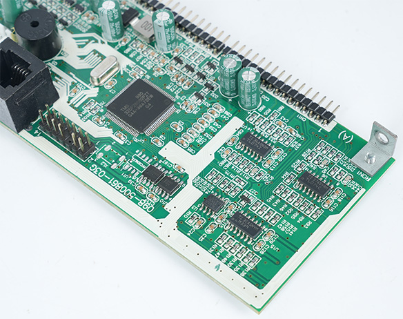
BGA soldering is not only a chip soldering process. In real PCBA manufacturing, BGA soldering quality is affected by PCB fabrication, stack-up design, surface finish, pad size, via-in-pad, solder paste printing, SMT placement, reflow profile, X-ray inspection, functional testing, and rework control.
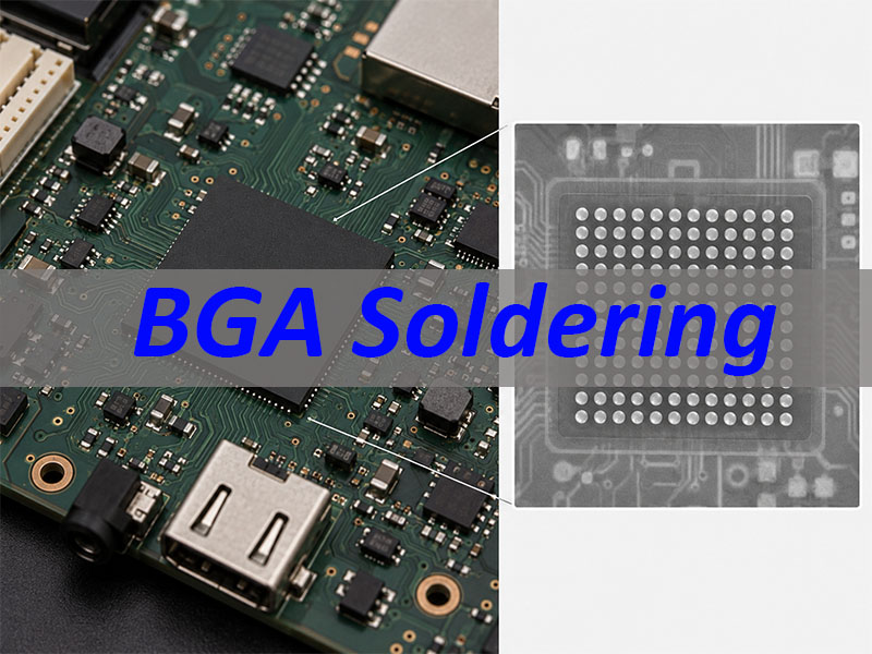
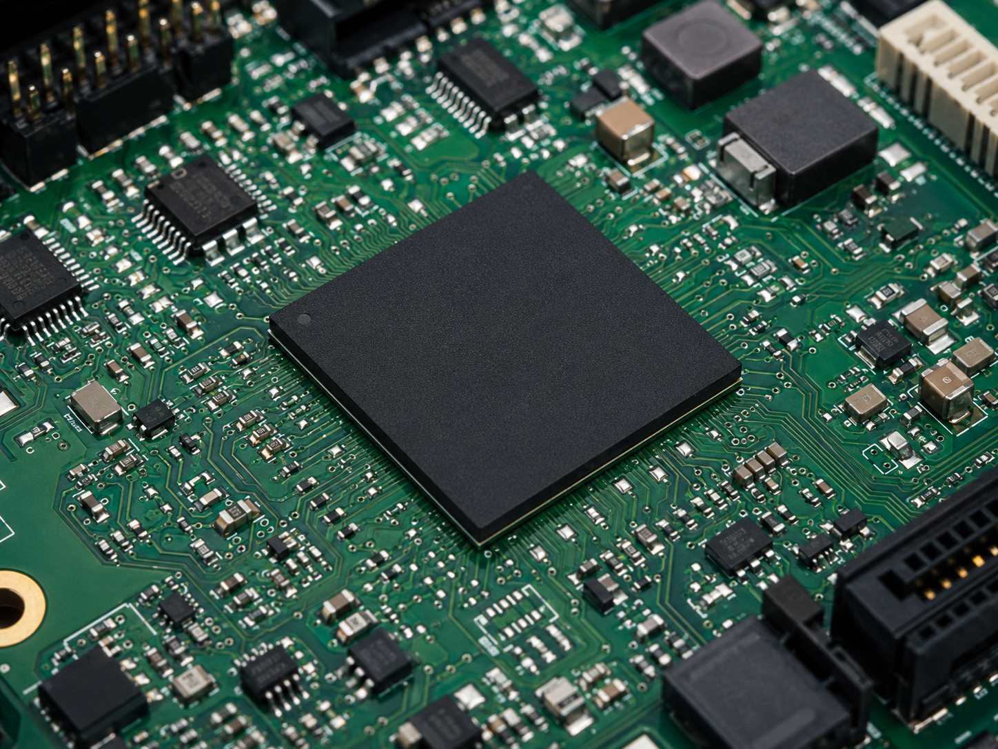
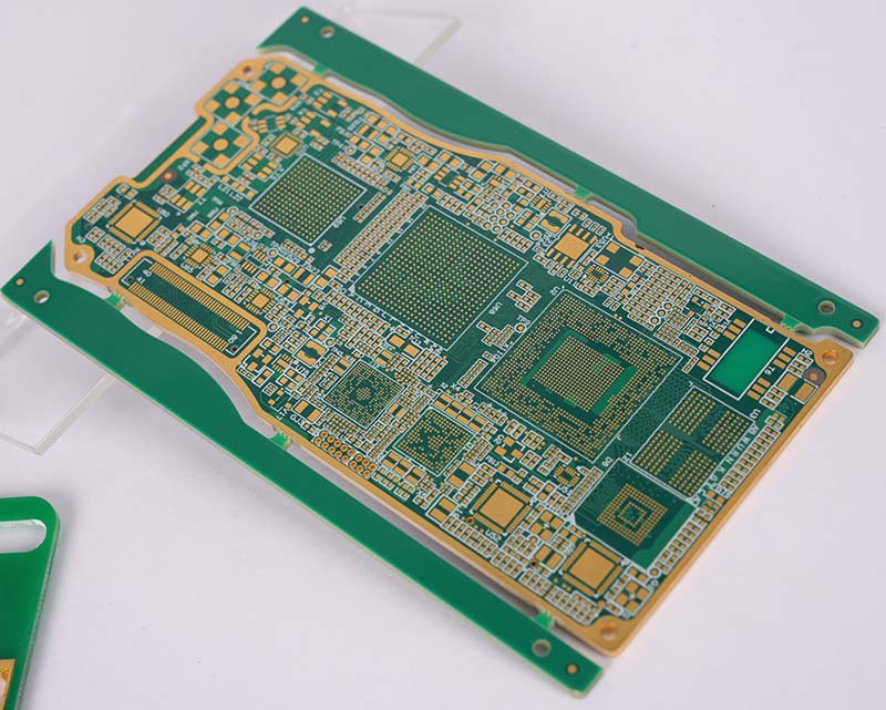
A BGA package hides its solder joints under the component body. This structure supports high-density PCB design and high pin-count ICs, but it also makes defects harder to detect. A BGA may look correctly placed from the outside while hidden solder joints still have opens, bridges, voids, or head-in-pillow defects.
This guide explains BGA soldering from a PCBA manufacturing quality perspective, helping engineers, hardware teams, and buyers understand how BGA soldering affects assembly yield, inspection, rework risk, and product reliability.
What Is BGA Soldering?
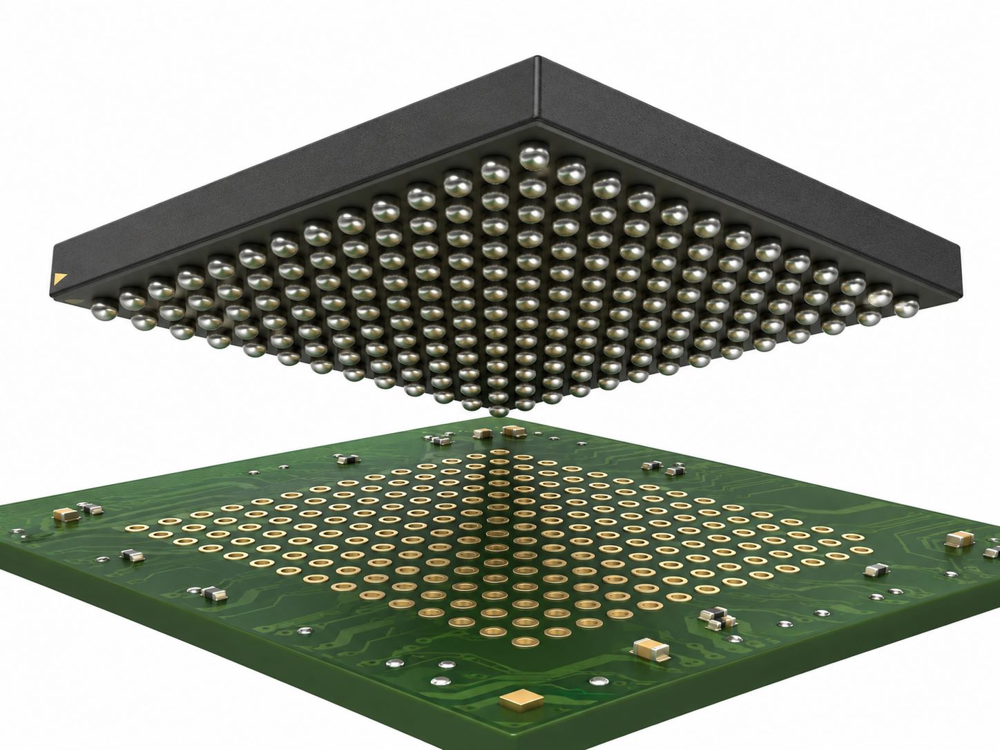
BGA soldering is the process of attaching a Ball Grid Array package to a PCB by melting solder balls between the component and the PCB pads during reflow soldering.
BGA stands for Ball Grid Array. Unlike leaded packages with visible pins around the package body, BGA components use solder balls arranged in a grid under the IC. During reflow, these solder balls melt, wet the PCB pads, and form electrical and mechanical connections.
BGA packages are commonly used in:
- Processors
- FPGAs
- Memory ICs
- Communication chips
- RF modules
- Automotive controllers
- Industrial control boards
- Medical electronics
- High-speed digital PCB assemblies
Common BGA pitch values include 1.0 mm, 0.8 mm, 0.65 mm, 0.5 mm, and 0.4 mm. As pitch becomes smaller, the process window becomes narrower.
For example:
- 1.0 mm / 0.8 mm BGA: easier to fan out and assemble.
- 0.5 mm BGA: needs tighter control of pad design, stencil opening, paste volume, and placement.
- 0.4 mm BGA: often requires early DFM review because solder mask registration, via strategy, bridging, and open-joint risk become more sensitive.
The main challenge is simple: BGA solder joints are hidden under the package. Therefore, BGA soldering must be controlled as a complete PCBA process, not only as a reflow step.
Why BGA Soldering Matters in PCBA Manufacturing?
BGA soldering matters because one hidden BGA defect can affect the entire PCBA, even when the board looks normal from the outside.
In PCBA manufacturing, BGA soldering connects multiple process areas:
- PCB stack-up
- HDI or via-in-pad design
- Pad size and surface finish
- Solder mask registration
- Stencil aperture design
- Solder paste printing
- SMT placement accuracy
- Reflow profile control
- X-ray inspection
- Functional testing
- Rework risk
A BGA defect is often not caused by one single step. It may start from PCB design or fabrication and only appear after SMT assembly.
Typical examples:
- Via-in-pad not filled properly: solder can wick into the via and cause insufficient solder.
- Poor pad flatness: BGA solder balls may not collapse evenly.
- Wrong stencil aperture: too much paste may cause bridging; too little may cause opens.
- Unverified reflow profile: a large BGA area may not reach proper solder joint temperature.
- Rigid-flex transition stress: local bending or warpage may affect nearby BGA joints.
- No X-ray inspection: hidden opens or voids may be missed before shipment.
For PCBA projects, BGA soldering quality is not only about “can the chip be soldered?” The better question is:
Can the BGA solder joints survive manufacturing, inspection, testing, shipment, and real product use?
How Does BGA Soldering Work in PCB Assembly?
BGA soldering works through solder paste printing, BGA placement, reflow heating, solder ball collapse, cooling, and hidden joint inspection.
A simplified BGA assembly flow is:
| Step | Main Control Point |
|---|---|
| Solder paste printing | Paste volume |
| SPI inspection | Paste height and area |
| BGA placement | X/Y alignment |
| Reflow soldering | Real solder joint temperature |
| Cooling | Joint solidification |
| X-ray inspection | Hidden solder joints |
| Electrical test | Opens and shorts |
| Functional test | Product-level behavior |
During reflow, the solder paste and BGA balls melt together. Molten solder has a self-centering effect, so a small placement offset may be corrected by surface tension. However, this effect has limits.
BGA self-alignment cannot fix major process problems.
It cannot fully correct:
- Wrong pad design
- Excessive placement offset
- Oxidized solder balls
- Poor solderability
- Wrong stencil aperture
- Severe PCB warpage
- Severe package warpage
- Insufficient reflow temperature
- Poor moisture control
For stable PCBA production, three areas must be controlled together.
Solder volume
- Too little solder may cause opens.
- Too much solder may cause bridging.
- Uneven solder volume may cause uneven solder ball collapse.
Thermal profile
- Too little heat may cause cold joints or incomplete wetting.
- Too much heat may damage components or PCB laminate.
- Uneven heating may cause warpage-related BGA defects.
Inspection
- AOI can check visible placement.
- X-ray is needed for hidden joint conditions.
- Electrical and functional testing confirm circuit behavior.
The process goal is not just to place the BGA correctly. The goal is to create stable hidden solder joints that pass manufacturing and product-level reliability requirements.
BGA Soldering Process: From PCB Fabrication to Reflow
A stable BGA soldering process starts before the SMT line. Many BGA soldering defects are created during PCB design, PCB fabrication, storage, stencil design, or solder paste printing before the board enters the reflow oven.
1. Review PCB fabrication requirements first
Before SMT assembly, the PCB must be suitable for BGA soldering.
Check:
- BGA pad diameter
- Solder mask opening
- ENIG thickness and surface flatness
- Via-in-pad filling and capping
- BGA fanout routing
- Stack-up and impedance requirements
- Board thickness and warpage
- Rigid-flex transition area
- Panel or single-board delivery method
For fine-pitch BGA, PCB fabrication quality directly affects soldering yield. SMT cannot fully correct poor pad design, poor via filling, poor flatness, or unstable impedance stack-up.
2. Control moisture before assembly
Many BGA packages are moisture-sensitive devices. If a moisture-sensitive package absorbs too much moisture before reflow, rapid heating may create internal vapor pressure. This can cause delamination, popcorning, package warpage, or soldering reliability problems.
A practical example:
- An MSL 3 component is commonly limited to 168 hours of floor life at ≤30°C / 60%RH after opening the moisture barrier bag.
- If the allowed floor life is exceeded, the component may need baking before reflow.
- If moisture control is ignored, even a correct reflow profile may still produce defects.
Moisture control matters because it can contribute to:
- Package warpage
- Open solder joints
- Head-in-pillow defects
- Delamination
- Popcorning
- Intermittent failures
3. Print solder paste accurately
Solder paste printing defines the starting solder volume. For BGA components, paste defects are difficult to repair after reflow because the final joints are hidden under the package.
Check:
- Stencil thickness
- Aperture design
- Paste volume
- Paste height
- Paste release
- Paste alignment
- Solder paste storage
- Solder paste expiration
- Printing speed and squeegee pressure
SPI is useful before placing expensive BGA components. It can detect insufficient paste, excess paste, bridging risk, and inconsistent deposits before reflow.
4. Place the BGA accurately
BGA placement requires accurate alignment between the solder ball array and PCB pads. Modern pick-and-place machines use vision systems to align the package and board.
Placement risks include:
- X/Y offset
- Wrong rotation
- Package tilt
- Excessive placement pressure
- Wrong nozzle selection
- Component movement before reflow
A small offset may appear acceptable before reflow, but after solder collapse it can become a hidden bridge or open joint.
5. Reflow with a verified board profile
The oven setting is not the same as the real solder joint temperature. Thick PCBs, heavy copper, large BGAs, shields, heatsinks, rigid-flex structures, and dense layouts can create temperature differences across the board.
For important BGA assemblies, the profile should be measured with thermocouples on a representative board. The key point is to verify what the actual BGA solder joints experience, not only what the oven program says.
BGA Soldering Temperature and Reflow Profile Control
BGA soldering temperature should be controlled according to the solder paste datasheet, solder alloy, BGA package limit, PCB thermal mass, component layout, and measured board profile. There is no single universal BGA soldering temperature.
For many lead-free SnAgCu-based BGA soldering processes, these reference values are commonly used during process setup:
| Reflow Parameter | Practical Reference |
|---|---|
| SAC-type solder liquidus reference | about 217°C |
| Lead-free BGA peak solder joint temperature | often around 235–245°C |
| Practical dwell above 217°C | often around 50–80 seconds |
| Excessive dwell above liquidus | increases thermal stress risk |
| Peak too low | poor wetting / insufficient collapse |
| Peak too high | component or PCB damage risk |
These values are not universal settings. They are starting references. The final profile must follow the solder paste datasheet, component reflow limit, and measured board-level temperature.
A typical BGA reflow profile has four zones.
| Zone | Purpose | If Poorly Controlled |
|---|---|---|
| Preheat | Gradual heating | Thermal shock |
| Soak | Flux activation and temperature equalization | Poor wetting or flux exhaustion |
| Reflow | Solder melting and joint formation | Cold joints or thermal damage |
| Cooling | Solder joint solidification | Stress or weak joint structure |
What matters in real PCBA production:
- Ramp rate
- Too fast: component and PCB stress increase.
- Too slow: flux may lose activity before reflow.
- Soak time
- Too short: temperature across the BGA may not equalize.
- Too long: flux activity may be consumed before full solder melting.
- Time above liquidus
- Too short: solder may not fully melt and wet.
- Too long: component and laminate stress increase.
- Peak solder joint temperature
- Too low: insufficient ball collapse or poor wetting.
- Too high: component damage, laminate damage, or excessive oxidation risk.
- Temperature difference across the BGA
- Large BGA packages may have different temperatures at corners and center.
- Uneven heating can lead to opens, head-in-pillow, or uneven collapse.
The better question is not “What temperature should the oven be set to?” The better question is:
What peak temperature and time above liquidus does the actual BGA solder joint reach on the real PCBA?
That is why professional BGA assembly uses profile verification instead of relying only on a generic oven program.
BGA Soldering Flux, Solder Paste, Pad Design, and Via-in-Pad
BGA soldering quality depends on solder paste, flux activity, stencil design, pad geometry, via structure, PCB surface finish, and PCB fabrication capability.
Solder paste controls solder volume and wetting behavior. Flux removes oxides and helps solder spread. Pad and via design determine how the molten solder forms the final joint.
Solder paste should match the BGA pitch and process.
Check:
- Alloy type
- Powder size
- Flux type
- Storage temperature
- Open time
- Printing life
- Reflow atmosphere
- Cleaning requirement
- Residue behavior
- Compatibility with BGA pitch
For fine-pitch BGA, solder paste volume control becomes more sensitive. A small paste printing error can create a large reliability risk because the solder balls are smaller and closer together.
Flux quality affects wetting.
Flux-related problems can cause:
- Poor wetting
- Solder balling
- Residue under BGA
- Leakage risk
- Head-in-pillow
- Incomplete solder joint formation
Expired paste, wrong storage, poor flux activity, or excessive soak time can all reduce wetting performance.
Pad and via design can prevent or create defects.
BGA pad design should consider:
- Pad diameter
- Solder mask opening
- NSMD or SMD pad style
- Surface finish
- Via-in-pad design
- Via filling and capping
- Escape routing
- Solder mask registration
- Pad flatness
For 0.5–0.8 mm pitch BGA using blind vias, some design references recommend blind via drill diameters of ≤0.004 in and an aspect ratio of ≤0.75:1. This should be treated as a design reference, not a universal rule for every PCB factory.
The practical meaning is more important:
- Fine-pitch BGA needs early DFM review.
- Do not finalize layout before checking PCB fabrication and assembly capability.
- Via-in-pad must be controlled.
- If a via under a BGA pad is not properly filled and capped, solder may wick into the via.
- This can create insufficient solder, voids, or open joints.
- Surface finish matters.
- ENIG is commonly used for BGA because it provides a flat solderable surface.
- Pad flatness and solderability are critical for fine-pitch BGA.
- Stencil design must match pad design.
- Pad size, aperture size, paste release, and solder volume should be reviewed together.
If the BGA pitch is 0.5 mm or smaller, the PCB designer, PCB fabricator, and SMT assembly team should review the stack-up, via strategy, solder mask, stencil, and inspection plan before production.
How to Inspect BGA Soldering Quality in PCBA?
BGA soldering quality should be inspected with X-ray, electrical testing, functional testing, and process data review. Visual inspection alone is not enough.
Because BGA solder joints are hidden under the package, normal optical inspection cannot fully verify the final solder connections.
Common inspection methods include:
| Method | Best Used For |
|---|---|
| SPI | Solder paste volume before placement |
| AOI | Visible placement and surface defects |
| X-ray | Hidden solder joints |
| Electrical test | Opens and shorts |
| Functional test | Product-level behavior |
| Cross-section | Failure analysis |
X-ray inspection is the key method for hidden BGA joints.
X-ray can help check:
- Solder shorts
- Insufficient solder
- Voids
- Potential opens
- Missing balls
- Ball collapse
- Alignment shift
- Abnormal solder shape
2D X-ray is commonly used for production monitoring. 3D X-ray or CT may be used when defects are difficult to confirm or when failure analysis requires more detail.
However, X-ray is not the same as functional proof.
X-ray may not fully prove:
- Intermittent opens
- Marginal wetting
- Mechanical weakness
- Thermal cycling reliability
- Correct component function
- Performance under real operating load
For high-reliability BGA assembly, inspection should combine:
- SPI before placement
- Verified reflow profile
- X-ray after reflow
- Electrical test
- Functional test
- Failure analysis for repeated defects
The inspection question should be:
Are the hidden joints physically acceptable, and does the assembled board work reliably?
Common BGA Soldering Defects and Root Causes
Most BGA soldering defects come from solder paste problems, poor wetting, reflow profile errors, warpage, pad design issues, contamination, or poor material handling.
| Defect | Common Trigger |
|---|---|
| Open joint | Low solder, warpage, poor wetting |
| Solder bridge | Excess solder, placement offset |
| Void | Flux outgassing, paste issue |
| Head-in-pillow | Warpage, oxidation, poor wetting |
| Cold joint | Low heat, short reflow time |
| Missing ball | Package damage or handling issue |
| Insufficient collapse | Poor reflow or solderability |
| Misalignment | Placement shift |
Open solder joints
An open joint means the solder ball does not form a continuous connection between the BGA and PCB pad.
Common causes:
- Insufficient solder paste
- Package warpage
- PCB warpage
- Poor wetting
- Pad contamination
- Low reflow temperature
- Poor coplanarity
Solder bridging
Solder bridging means adjacent solder balls are connected by excess solder.
Common causes:
- Too much solder paste
- Poor stencil design
- Placement offset
- Pad design error
- Fine-pitch layout risk
- Excessive solder collapse
Voids
Voids are gas pockets inside solder joints. Some voiding may be acceptable depending on the product requirement, but excessive voiding can reduce thermal and mechanical reliability.
Common causes:
- Flux outgassing
- Poor paste condition
- Via-in-pad issue
- Pad contamination
- Inappropriate reflow profile
Head-in-pillow
Head-in-pillow is a serious BGA defect where the solder ball and solder paste touch but do not fully merge.
Common causes:
- Package warpage
- PCB warpage
- Oxidized solder balls
- Poor flux activity
- Insufficient paste contact
- Inappropriate thermal profile
Cold solder joints
Cold joints occur when solder does not fully melt or wet properly.
Common causes:
- Low peak temperature
- Short time above liquidus
- Excessive board thermal mass
- Wrong reflow profile
- Poor solderability
Warpage-related failure
Large BGA packages can warp during reflow. The PCB can also warp. If the package and board separate during the critical melting stage, some joints may not form correctly.
To reduce BGA defects before production, control:
- Moisture storage
- PCB baking when required
- Component baking when required
- Solder paste storage
- Stencil design
- Paste printing
- Placement accuracy
- Reflow profile
- X-ray criteria
- Functional test plan
- Rework limits
BGA Soldering in Real PCBA Projects: Three Practical Cases
BGA soldering becomes more meaningful when it is discussed inside real PCBA structures. The risk is different for a 2-layer FPC, a 6-layer rigid-flex PCB, and a 6-layer FR4 impedance-controlled PCB.
The following examples show how board structure changes BGA soldering risk and process control.
Case 1: 2L FPC with BGA Area, 1 oz Copper, ENIG, Panel Delivery
Board parameters:
- 2-layer FPC
- 1 oz copper
- ENIG surface finish
- Panel delivery
- Front side upper BGA area: white solder mask, no coverlay
- Front side lower area: 1 mil white coverlay
- Back side: full 1 mil white coverlay
This is not a standard rigid PCB BGA case. It is a flexible circuit with a local BGA soldering area. The key risk is not only soldering the BGA. The key risk is maintaining flatness, support, and solder joint stability in a flexible structure.
Main risks:
- FPC may deform during SMT if support is not enough.
- 1 oz copper increases stiffness and heat spreading compared with thinner FPC copper.
- The BGA area uses white solder mask instead of coverlay, so the transition between solder mask and coverlay must be controlled.
- Coverlay edge near the BGA area may create height difference or stress concentration.
- Panel delivery helps SMT handling, but the panel still needs proper fixture support.
- BGA joints cannot be checked by visual inspection.
Recommended PCBA controls:
- Review whether the BGA area needs a stiffener or SMT carrier fixture.
- Keep coverlay openings and coverlay edges away from critical BGA soldering areas.
- Confirm ENIG pad flatness and solderability before SMT.
- Use SPI to confirm solder paste volume before BGA placement.
- Verify reflow profile on the actual FPC panel, not only on a rigid board.
- Use X-ray inspection after reflow.
- Control depaneling and handling stress after SMT.
For this type of FPC project, the BGA risk is closely related to flexible material behavior. The SMT process must prevent bending, local lift, and unstable solder joint collapse.
Case 2: 6L Rigid-Flex PCB with BGA, Impedance, 0.2 mm PTH Tolerance, DP190 Adhesive
Board parameters:
- 6-layer rigid-flex PCB
- 0.5 oz copper
- ENIG surface finish
- Total thickness: 1.0 mm
- Rigid area: FR4 Tg170
- Solder mask: blue solder mask, white legend
- Flex area: black coverlay
- Outline tolerance: +0.003 in / -0.003 in
- Production cycle and UL94V marking required
- 0.2 mm PTH hole tolerance: ±2 mil
- BGA and impedance control required
- Impedance test report required
- SMT required
- Single-board delivery after SMT
- Rigid-flex transition area needs DP190 adhesive
This is a high-risk PCBA structure because BGA soldering, rigid-flex mechanics, impedance control, tight PTH tolerance, SMT, and adhesive dispensing are combined in one project.
Main risks:
- Rigid-flex transition stress may affect nearby BGA solder joints.
- 1.0 mm total thickness means the board may be more sensitive to handling and support during SMT.
- BGA and impedance routing must be controlled through stack-up and fabrication.
- 0.2 mm PTH with ±2 mil tolerance is tighter than normal hole tolerance and must be checked against drill and plating capability.
- DP190 adhesive must be controlled so it does not contaminate soldering areas or affect assembly flatness.
- Single-board delivery after SMT increases the importance of safe depaneling and handling.
Recommended PCBA controls:
- Review rigid-flex stack-up before fabrication.
- Confirm impedance structure and test coupon design before production.
- Verify whether the 0.2 mm PTH ±2 mil requirement can be held for the required hole group.
- Check BGA fanout, pad size, solder mask opening, and via strategy.
- Use fixture support during SMT to reduce flex-rigid movement.
- Measure reflow profile near the BGA area and near the rigid-flex transition.
- Use X-ray inspection for BGA joints after reflow.
- Control DP190 dispensing area, amount, and curing condition.
- Provide impedance test report after PCB fabrication.
- Run functional test after SMT if the product requires it.
For this project, the BGA problem is not isolated. It is connected with rigid-flex design, hole tolerance, impedance, adhesive process, and SMT handling. This type of PCBA should be reviewed before PCB fabrication, not only before assembly.
Case 3: 6L FR4 Tg170 PCB with BGA, Differential Impedance, ENIG 1u”, and SMT
Board parameters:
- 6-layer PCB
- FR4 Tg170
- Board thickness: 1.6 mm ±10%
- Inner copper: 1 oz
- Outer copper: 0.5 oz before plating
- ENIG surface finish, gold thickness 1u”
- Blue solder mask, white legend
- Production cycle and UL94V marking required
- Differential impedance required
- Impedance report required
- BGA required
- SMT required
- Single-board delivery after SMT
This is a more typical rigid PCB BGA PCBA project, but it still needs careful control because BGA and differential impedance are both present.
Main risks:
- Differential impedance depends on stack-up, dielectric thickness, copper thickness, and trace geometry.
- BGA fanout may affect routing space for differential pairs.
- ENIG 1u” provides a flat solderable finish, but surface finish thickness and pad quality still need control.
- 6-layer FR4 Tg170 with 1.6 mm thickness has more stable mechanical support than FPC, but thermal mass still affects reflow profile.
- Single-board delivery after SMT requires stress control during routing, separation, cleaning, packing, and shipment.
Recommended PCBA controls:
- Confirm stack-up and impedance table before PCB fabrication.
- Verify impedance test coupon and provide impedance report.
- Check BGA pad diameter and solder mask opening.
- Review whether BGA escape routing affects differential pair spacing.
- Verify ENIG thickness and pad solderability.
- Use SPI before placement if BGA pitch or IC value is high.
- Verify reflow profile on the real 6L board.
- Use X-ray inspection after BGA soldering.
- Confirm final functional test requirements before mass production.
Compared with the rigid-flex case, this FR4 PCB is easier to support during SMT. However, because it has both BGA and differential impedance, fabrication and assembly still need to be controlled together.
What These Three Cases Show
These cases show that BGA soldering is never just one SMT step.
- On 2L FPC, the main concern is flexible material support, coverlay transition, and BGA area flatness.
- On 6L rigid-flex PCB, the main concern is rigid-flex stress, tight PTH tolerance, impedance, BGA inspection, and DP190 adhesive control.
- On 6L FR4 PCB, the main concern is stack-up, differential impedance, BGA pad quality, ENIG surface finish, and verified reflow profile.
In all three cases, BGA quality depends on PCB fabrication and PCBA process control working together.
Why Choose EBest Circuit for BGA PCB Assembly?
Choose EBest Circuit for BGA PCB assembly when your project needs both PCB manufacturing control and PCBA process control.
BGA soldering is not only an SMT capability. It also requires PCB fabrication capability, stack-up control, surface finish control, pad accuracy, drilling capability, impedance control, reflow process control, X-ray inspection, and functional testing.
Based on our PCB process capability, EBest Circuit supports key manufacturing requirements related to BGA and PCBA projects.
PCB manufacturing capability for BGA projects
| Capability Item | EBest Circuit Capability |
|---|---|
| Standard PCB layer count | 1–50L |
| Engineering review layer count | up to 100L |
| Standard board thickness range | 0.4–6.0 mm |
| Extreme board thickness range | 0.15–10 mm |
| High Tg FR4 materials | Tg170–180 options available |
| Minimum laser drill | 0.10 mm standard |
| Minimum mechanical drill | 0.15 mm |
| Standard PTH hole tolerance | ±0.076 mm |
| BGA pad minimum | 10 mil standard |
| BGA pad minimum with ENIG | 8 mil |
| ENIG gold thickness | 0.025–0.125 μm |
| ENIG nickel thickness | 3–8 μm |
| Impedance tolerance | ±5Ω below 50Ω; ±10% at 50Ω and above |
| Standard outline tolerance | ±0.13 mm |
| CNC outline tolerance, reviewed cases | ±0.10 mm |
| Warpage capability | 0.75% standard, 0.5% reviewed cases |
Why this matters for BGA PCBA
- BGA pad capability matters
- Smaller BGA pads need tighter fabrication control.
- ENIG can support smaller BGA pads and provides a flatter solderable surface.
- Impedance capability matters
- Many BGA chips are used in high-speed PCB designs.
- Differential impedance must be controlled through stack-up, copper thickness, trace width, spacing, and test coupons.
- Drilling capability matters
- Fine-pitch BGA may require microvias, blind vias, or via-in-pad.
- Poor via design can cause solder wicking, opens, voids, or insufficient solder.
- High Tg material matters
- FR4 Tg170 is useful for boards that need better heat resistance during assembly and operation.
- BGA, reflow soldering, and high-reliability PCBA projects often require more stable laminate choices.
- Surface finish matters
- ENIG is commonly used for BGA because it provides a flat solderable surface.
- Surface finish thickness, pad flatness, and solderability should be controlled before SMT.
- PCBA process control matters
- BGA solder joints are hidden.
- X-ray inspection, reflow profile verification, and functional testing are important for reliable delivery.
For BGA PCBA projects, EBest Circuit can support PCB fabrication, DFM review, SMT assembly, BGA soldering, X-ray inspection, impedance control, and turnkey PCBA service. If your project includes FPC BGA, rigid-flex BGA, HDI BGA, impedance-controlled BGA, or high-value IC assembly, pls feel free to send your Gerber files, BOM, pick-and-place file, assembly drawing, impedance requirements, and test requirements to sales@bestpcbs.com.
FAQs About BGA Soldering
What is BGA soldering?
BGA soldering is the process of attaching a Ball Grid Array package to a PCB by melting solder balls under the component during reflow soldering.
How is a BGA chip soldered to a PCB?
A BGA chip is placed on solder paste printed on PCB pads. During reflow, the solder paste and BGA balls melt, wet the pads, and form hidden solder joints.
What temperature is used for BGA soldering?
Lead-free BGA reflow commonly uses solder joint temperatures around 235–245°C, with SAC-type solder liquidus often referenced around 217°C. The final profile must follow the solder paste datasheet, component limits, and measured board temperature.
How long should BGA stay above liquidus?
For lead-free BGA soldering, some process references use about 50–80 seconds above 217°C as a practical dwell range. The correct value depends on solder paste, component type, PCB thickness, thermal mass, and profile measurement.
Can BGA be soldered by hand?
Some BGA rework can be done by experienced technicians using proper equipment, but reliable BGA assembly should not rely on hand soldering. Hidden joints require controlled heating and inspection.
Can you solder BGA with hot air?
Hot air can be used for some BGA rework, but uncontrolled hot air increases the risk of uneven heating, pad damage, warpage, and poor repeatability. A professional BGA rework station provides better control.
How do you inspect BGA solder joints?
BGA solder joints are usually inspected by X-ray, electrical testing, functional testing, and sometimes cross-section analysis. Visual inspection alone is not enough.
What are common BGA soldering defects?
Common BGA soldering defects include open joints, solder bridges, voids, head-in-pillow, cold joints, misalignment, missing balls, and warpage-related failures.
Is X-ray inspection required for BGA soldering?
For reliable BGA assembly, X-ray inspection is strongly recommended because BGA solder joints are hidden under the package.
What is the difference between BGA reflow and BGA rework?
BGA reflow soldering is the original SMT PCBA process. BGA rework is a repair process used to remove, replace, reball, or repair a BGA component after assembly.
Need reliable BGA PCB assembly with DFM review, SMT assembly, X-ray inspection, and functional testing? Pls feel free to send your Gerber files, BOM, pick-and-place file, and assembly requirements to EBest Circuit at sales@bestpcbs.com.