A 10 layer PCB stackup is used when a board has dense routing, high-speed signals, several power rails and strict signal integrity needs. The right stackup controls impedance, shortens return paths and reduces crosstalk.
For high-speed PCB design, more layers alone do not guarantee better performance. The stackup should use solid ground planes, controlled dielectric spacing, balanced copper and realistic impedance targets. These details help the PCB perform well in both testing and mass production.
What Is a 10 Layer PCB Stackup?
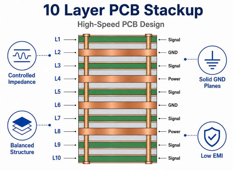
A 10 layer PCB stackup is a multilayer PCB structure with ten copper layers separated by core and prepreg materials. These copper layers are arranged as signal layers, ground planes, power planes or mixed routing layers.
The stackup controls how signals, power and return current move through the board. It also affects impedance, EMI, board thickness, thermal behavior and production yield.
A good 10-layer structure should clearly define layer order, copper weight, dielectric thickness, material type, GND plane position, power plane position and impedance targets. Without these details, the PCB may pass layout review but fail during testing or production.
What Is a Standard 10 Layer PCB Stackup?
A standard 10 layer PCB stackup usually places signal layers close to ground planes. This gives high-speed traces a stable return path and leaves enough layers for power distribution and component fanout.
A common structure is:
| Layer | Type | Function |
|---|---|---|
| L1 | Signal | Components and short routing |
| L2 | GND | Reference plane |
| L3 | Signal | Inner signal routing |
| L4 | Power | Power distribution |
| L5 | GND | Shielding and return path |
| L6 | GND | Shielding and return path |
| L7 | Power | Power distribution |
| L8 | Signal | Inner signal routing |
| L9 | GND | Reference plane |
| L10 | Signal | Components and low-speed routing |
This structure is widely used because it provides multiple ground references, good shielding and balanced lamination. However, the final layer order should still match the signal speed, power rails, BGA density and PCB factory capability.
What Is a Practical 10 Layer PCB Stackup Example?
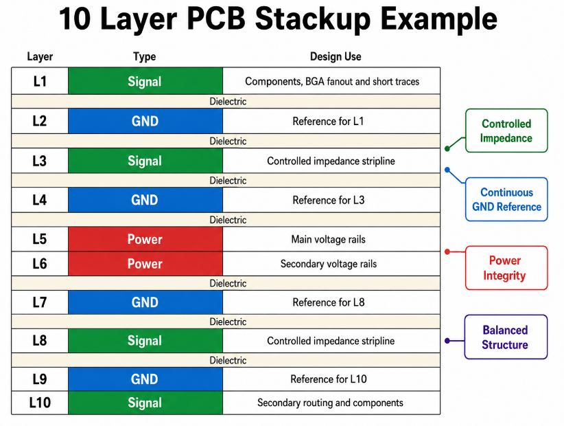
A practical 10 layer PCB stackup example should show how each layer supports routing, power integrity and production stability. For high-speed PCB design, critical signals should be placed next to continuous GND planes.
A practical PCB 10 layer stackup example is:
| Layer | Type | Design Use |
|---|---|---|
| L1 | Signal | Components, BGA fanout and short traces |
| L2 | GND | Reference for L1 |
| L3 | Signal | Controlled impedance stripline |
| L4 | GND | Reference for L3 |
| L5 | Power | Main voltage rails |
| L6 | Power | Secondary voltage rails |
| L7 | GND | Reference for L8 |
| L8 | Signal | Controlled impedance stripline |
| L9 | GND | Reference for L10 |
| L10 | Signal | Secondary routing and components |
This structure gives four GND layers, two power layers and four signal layers. It is suitable for high-speed interfaces, dense routing and controlled impedance layouts.
How Should Ground and Power Planes Be Arranged in a 10 Layer PCB Stackup?
Ground and power planes should be arranged to give high-speed signals short return paths, stable voltage delivery and low EMI risk. In a 10 layer PCB stackup, ground planning should come before adding more routing space.
- Place high-speed signal layers next to solid GND planes.
A nearby GND plane gives the return current a direct path under the trace. This reduces loop area, signal reflection and radiation noise. - Use more than one GND plane when the design has fast signals.
A strong 10-layer high-speed PCB often uses three to four GND planes. This improves shielding and helps separate noisy circuits from sensitive signals. - Keep power and GND planes close where possible.
Closely spaced power and ground planes improve plane coupling and help reduce power noise. This is useful for processors, FPGAs, DDR memory and communication chips. - Avoid routing high-speed traces over split planes.
If a trace crosses a gap in the reference plane, the return current is forced to detour. This can create EMI, impedance discontinuity and timing problems. - Place noisy power areas away from sensitive signal layers.
Switching regulators, high-current rails and fast digital circuits should not share weak or broken reference areas with sensitive signal routes. - Keep the whole stackup symmetrical.
Balanced copper and even dielectric distribution reduce bow, twist and lamination stress during PCB manufacturing. - Use stitching vias near layer transitions.
When high-speed signals change layers, nearby GND stitching vias help the return current move smoothly between reference planes. - Do not use broken power islands as the main high-speed reference.
A continuous GND plane is usually safer than a fragmented power plane because return current is easier to control.
How Does Dielectric Thickness Affect a 10 Layer PCB Stackup?
Dielectric thickness affects impedance, trace width, crosstalk and total PCB thickness. In a 10 layer PCB stackup, the distance between a signal trace and its reference plane directly changes the electrical behavior of the trace.
A thinner dielectric gives stronger coupling between the signal trace and the GND plane. This helps create a shorter return path, lower EMI risk and narrower controlled-impedance traces.
A thicker dielectric weakens coupling and usually requires wider traces to reach the same impedance. This can reduce routing space around BGAs, fine-pitch ICs and dense connectors.
Dielectric thickness should not be guessed during layout. It should be confirmed with the PCB manufacturer because real prepreg thickness can change after lamination due to resin flow, copper coverage and press conditions.
How to Design a 10 Layer PCB Stackup for Impedance Control?
To design a 10 layer PCB stackup for impedance control, start with signal requirements and manufacturing limits. The goal is to make the designed impedance match the real PCB after lamination, etching and plating.
- Confirm the impedance targets first.
Common values include 50Ω single-ended, 90Ω differential and 100Ω differential, depending on the signal interface. - Choose the routing structure.
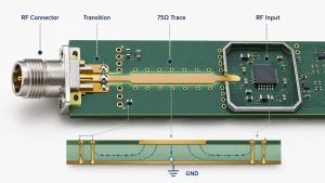
Use microstrip for outer-layer routing and stripline for inner-layer routing. Stripline usually gives better shielding, while microstrip is easier to access during layout review. - Assign clean reference planes.
Each controlled-impedance layer should reference a continuous GND plane. Avoid plane cuts, voids and split areas under high-speed traces. - Define dielectric thickness before routing.
Trace width depends on the distance between the signal layer and the reference plane. If the dielectric changes later, impedance may also change. - Use the correct material Dk.
Dk should match the working frequency range, not only the material name. High-speed designs may require lower-loss materials when signal loss becomes critical. - Control trace width and spacing together.
Differential pairs depend on both trace width and pair spacing. Changing only one value may cause impedance drift or layout mismatch. - Include finished copper thickness.
Finished copper is affected by base copper, plating and etching. Wrong copper assumptions can change the final impedance result. - Avoid unnecessary layer changes.
Each via transition can create impedance discontinuity. When layer changes are required, use proper via design and nearby GND stitching vias. - Request impedance coupons.
Test coupons help verify whether the finished PCB matches the required impedance tolerance after fabrication. - Let the PCB factory review the stackup before release.
The final structure should match actual laminate, prepreg, copper and process capability.
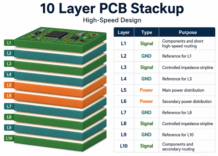
What Is the Best 10 Layer PCB Stackup for High-Speed Design?
The best 10 layer PCB stackup for high-speed design is a balanced structure with continuous GND planes beside critical signal layers, stable power-plane placement and controlled dielectric spacing.
A strong high-speed structure is:
| Layer | Type | Purpose |
|---|---|---|
| L1 | Signal | Components and short high-speed routing |
| L2 | GND | Reference for L1 |
| L3 | Signal | Controlled impedance stripline |
| L4 | GND | Reference for L3 |
| L5 | Power | Main power distribution |
| L6 | Power | Secondary power distribution |
| L7 | GND | Reference for L8 |
| L8 | Signal | Controlled impedance stripline |
| L9 | GND | Reference for L10 |
| L10 | Signal | Components and secondary routing |
This structure works well because it gives high-speed signals clear return paths, strong shielding, lower crosstalk and better EMI control. It also keeps the board more balanced during lamination.
How to Use a 10 Layer PCB Stackup Calculator?
A 10 layer PCB stackup calculator helps estimate trace width, spacing and dielectric height for controlled impedance. It is useful at the early design stage, but the final result should always be checked by the PCB manufacturer.
- Select the right trace model.
Choose microstrip for outer layers and stripline for inner layers. Using the wrong model can give misleading impedance values. - Enter dielectric thickness accurately.
Use the real distance from the signal trace to its reference plane. Do not use total board thickness for impedance calculation. - Enter finished copper thickness.
Finished copper includes base copper and plating. This value affects trace geometry and impedance. - Use the correct material Dk.
Dk should come from the selected laminate and working frequency range. A generic FR-4 value may not be accurate for high-speed designs. - Set the target impedance.
Enter 50Ω single-ended, 90Ω differential or 100Ω differential according to the signal standard. - Adjust trace width and spacing within factory capability.
Very narrow traces or tight spacing may look correct in the calculator but may reduce production yield. - Check both outer and inner layers separately.
Outer-layer microstrip and inner-layer stripline usually require different trace widths for the same impedance target. - Send the result for factory review.
Calculator values are estimates. Final impedance depends on material tolerance, etching accuracy, plating thickness, solder mask and lamination control.
What Problems Can Happen in a Poor 10 Layer PCB Stackup?
A poor 10 layer PCB stackup can cause electrical failure, EMI issues and production instability. Most problems appear when signal layers lack clean references, dielectric thickness is wrong or copper distribution is unbalanced.
- Impedance mismatch.
Wrong trace width, dielectric spacing or copper thickness can cause impedance drift. This may lead to signal reflection, eye diagram failure and unstable communication. - Crosstalk between signal layers.
If high-speed traces are routed too close or stacked without proper GND shielding, signals can interfere with each other. - EMI radiation.
Long return paths and split reference planes create large current loops. These loops can increase radiated noise and cause EMI test failure. - Power noise.
Weak power and GND plane coupling can increase voltage ripple. This affects processors, memory, RF modules and high-speed interfaces. - BGA escape routing problems.
Poor layer planning can make dense BGA fanout difficult. This may force risky trace spacing, extra vias or unnecessary routing detours. - Board warpage.
Unbalanced copper, uneven dielectric spacing or poor layer symmetry can increase bow and twist during lamination and assembly. - Higher signal loss.
Unsuitable dielectric material or rough copper can increase insertion loss, especially in fast digital and communication designs. - Low manufacturing yield.
If the stackup requires traces, spacing or dielectric values beyond factory capability, production may face more defects and higher cost. - Poor repeatability in batch production.
A stackup that works once may fail in volume if material, lamination and impedance tolerance are not controlled.
What Should Be Checked Before Manufacturing a 10 Layer PCB Stackup?
Before manufacturing a 10 layer PCB stackup, the design should be checked against real production capability. The review should cover electrical performance, material selection, mechanical balance and inspection requirements.
- Final layer order: Confirm each signal, GND and power layer position.
- Reference planes: Check whether every high-speed signal layer has a continuous reference plane.
- Board thickness: Confirm finished thickness and tolerance.
- Core and prepreg: Verify material type, dielectric thickness and lamination structure.
- Copper weight: Confirm base copper and finished copper thickness.
- Impedance targets: List single-ended and differential values clearly.
- Impedance tolerance: Confirm whether the project uses standard or tighter tolerance.
- Trace width and spacing: Check whether values match factory capability.
- Differential pairs: Confirm pair width, pair spacing and length-matching rules.
- Via structure: Review through vias, blind vias, buried vias, microvias and via-in-pad needs.
- BGA fanout: Confirm escape routing feasibility before production.
- Copper balance: Check whether copper distribution is balanced across the board.
- Warpage risk: Review board thickness, copper balance and panel layout.
- Solder mask: Confirm solder mask opening, bridge capability and outer-layer impedance effect.
- Surface finish: Choose ENIG, HASL, immersion silver, OSP or other finish based on assembly needs.
- Impedance coupons: Confirm coupon design and test method.
- Electrical test: Confirm netlist test requirements.
- Inspection reports: Confirm AOI, microsection, impedance test and final quality records.
- Assembly requirements: Check panelization, fiducials, component clearance and soldering process needs.
FAQs About 10 Layer PCB Stackup
Q1: What is the common finished thickness for a 10-layer PCB?
A1: Many 10-layer PCBs use 1.6mm finished thickness, but this is not fixed. High-speed PCB design may use a different thickness to meet impedance, connector, enclosure or mechanical strength requirements. The final value should be confirmed with dielectric spacing, copper thickness and lamination tolerance before layout release.
Q2: Is a 10-layer PCB always better than an 8-layer PCB?
A2: No. A 10-layer PCB is better only when the design requires more routing space, more reference planes, better power distribution or stronger EMI control. An 8-layer PCB may work well for simpler circuits. The decision should depend on signal speed, BGA density, power rails, board size and cost target.
Q3: When should a 10 layer HDI PCB stackup be used?
A3: A 10 layer HDI PCB stackup should be used when fine-pitch BGAs, compact board size or dense routing make through-hole vias difficult. HDI can use blind vias, buried vias, microvias and via-in-pad structures. It improves routing density, but it also increases cost, lamination steps and process control requirements.
Q4: What is the difference between microstrip and stripline in a 10-layer PCB?
A4: Microstrip traces are usually routed on outer layers and reference one plane below them. Stripline traces are routed inside the PCB and are placed between reference planes. Stripline gives better shielding, while microstrip is easier to inspect and adjust during layout review.
Q5: Does solder mask affect controlled impedance?
A5: Yes. Solder mask can affect outer-layer microstrip impedance because it changes the dielectric environment around the trace. The effect is usually smaller than dielectric thickness or trace width, but it still matters for tight impedance control. For sensitive designs, solder mask data should be included in the impedance model.
Q6: What impedance tolerance is common for 10-layer PCBs?
A6: Many controlled impedance PCB projects use ±10% tolerance as a common production target. Tighter tolerance may be possible, but it depends on material control, etching accuracy, copper thickness, dielectric tolerance and testing method. For high-speed interfaces, tolerance should be confirmed before fabrication.
Q7: What materials are used in a 10-layer PCB?
A7: A 10-layer PCB usually uses copper foil, core, prepreg, solder mask and surface finish. Standard FR-4 can be used for many digital boards, while high-speed designs may require high-Tg FR-4 or low-loss laminate. Material choice should consider Dk, Df, Tg, copper roughness and assembly temperature.
Q8: What files are required for 10-layer PCB stackup review?
A8: A complete review should include Gerber files, drill files, stackup drawing, impedance table, material requirements, copper weight, finished thickness, via structure and special notes. For controlled impedance designs, provide single-ended and differential impedance targets so the PCB factory can check manufacturability before production.
Q9: Can one standard 10-layer stackup fit all high-speed designs?
A9: No. A standard 10 layer PCB stackup can be a useful starting point, but each project should be adjusted for signal speed, BGA pitch, impedance targets, power rails, material loss and board thickness. A design for DDR, Ethernet, PCIe or RF may require different layer spacing and routing rules.
Q10: How does copper thickness affect a 10-layer PCB stackup?
A10: Copper thickness affects trace width, impedance, current capacity, heat spreading and etching accuracy. Thicker copper can carry more current, but it may make fine-line impedance routing harder. For high-speed boards, finished copper thickness should be defined clearly because plating and etching variation can change the final impedance result.
Q11: Why does BGA pitch matter in a 10-layer PCB stackup?
A11: BGA pitch affects escape routing, via size, trace spacing and layer count. Fine-pitch BGAs may require microvias, via-in-pad or HDI buildup. If BGA fanout is not checked early, the layout may require more layers, tighter spacing or expensive process changes during PCB fabrication.
Q12: How can a supplier prove 10-layer PCB quality?
A12: A reliable supplier should provide stackup review, material traceability, AOI, electrical testing, impedance testing, microsection inspection and final inspection records. For batch production, repeatable lamination control and stable impedance data are more important than a low first quote.
Q13: What affects the cost of a 10-layer PCB?
A13: Cost is affected by board size, material grade, copper thickness, impedance control, HDI structure, via-in-pad, surface finish, solder mask type, test requirements and order quantity. A simple 10-layer board costs less than a high-speed HDI board with tight tolerance and low-loss laminate.
Q14: Can EBest provide 10-layer PCB assembly after fabrication?
A14: Yes. EBest Circuit can support 10-layer PCB fabrication and PCBA assembly for custom, OEM/ODM and batch production projects. Assembly support can include component sourcing, SMT assembly, through-hole assembly, functional testing, inspection reports and global delivery from a China-based source factory.
Conclusion
The best 10-layer PCB structure for high-speed PCB design should combine solid GND references, controlled dielectric spacing, suitable materials, balanced copper and verified impedance targets. A good stackup reduces signal risk before layout problems become expensive to fix.
For project selection, check signal speed, impedance values, BGA density, material loss, board thickness, power rails and assembly requirements before finalizing the stackup. For procurement, compare the supplier’s review ability, impedance testing, material traceability, production records and PCBA support, not only the board price.
EBest Circuit provides 10-layer PCB manufacturing and assembly services for high-speed, industrial, communication, medical, automotive and custom electronic projects. If you need stackup review, controlled impedance fabrication, HDI production, PCBA assembly or a batch quotation, send your files to sales@bestpcbs.com.