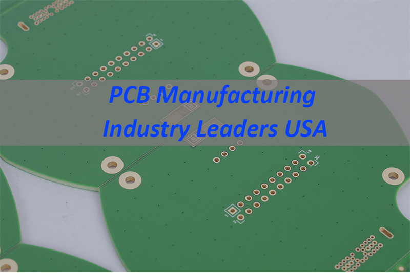
Choosing from the top PCB manufacturers is not just about the biggest name or the lowest online price. A useful supplier list should help engineers and buyers find the right fit for the board type, technical risk, order volume, and delivery plan.
A simple FR4 prototype, HDI PCB, metal core LED board, rigid-flex PCB, and turnkey PCBA project all need different supplier strengths. EBest Circuit (Best Technology) supports custom PCB manufacturing, component sourcing, PCBA assembly, DFM review, and testing. If you are comparing PCB manufacturers for a new project, send your Gerber files, stackup, BOM, drawings, or assembly notes to sales@bestpcbs.com for an engineering review before production.
What Makes the Top PCB Manufacturers Different?
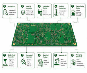
The top PCB manufacturers differ in four areas: project fit, engineering support, production capability, and quality control. A buyer should compare these points before looking at price.
Project fit
- Some manufacturers are built for online prototypes. Some are better for HDI, rigid-flex, or special materials. Others are stronger in PCBA assembly or larger production programs. The best supplier is the one that fits the actual project stage.
Engineering support
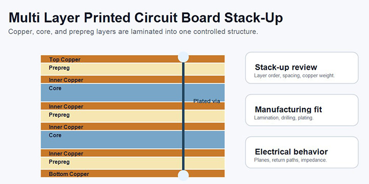
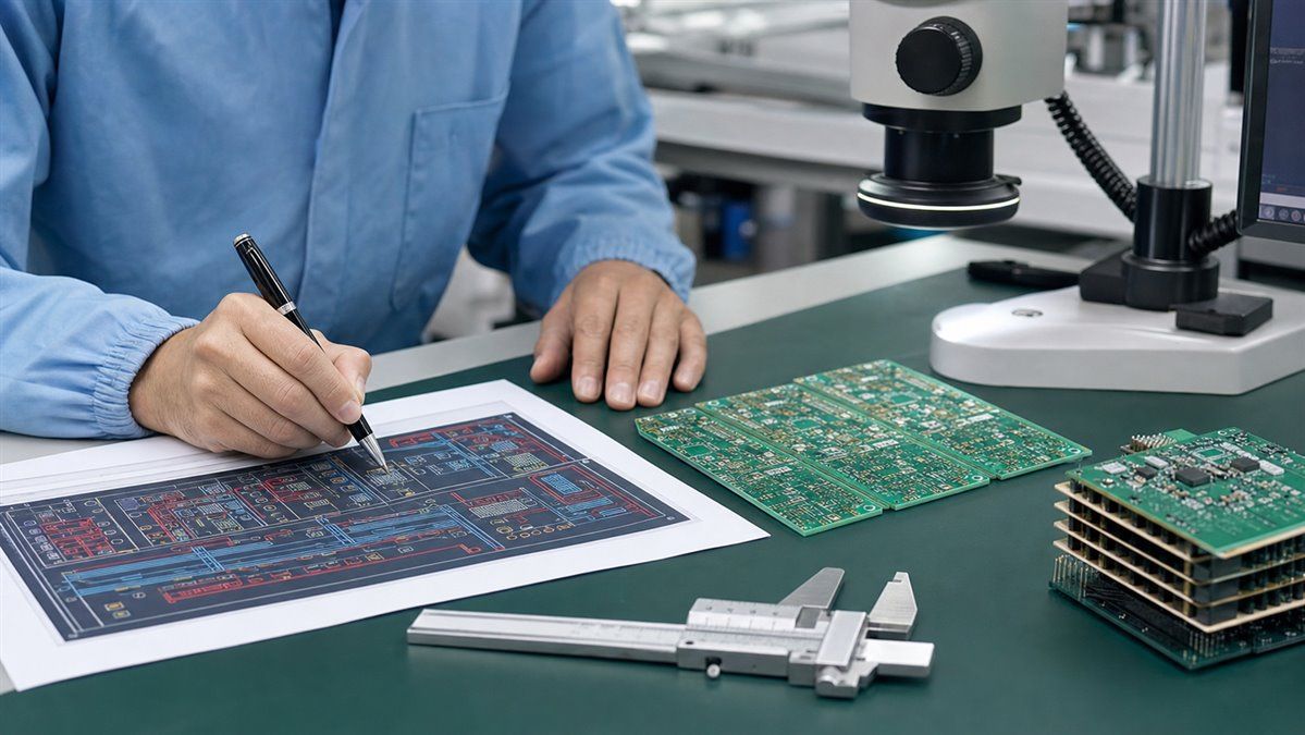
- For simple prototypes, an automated file check may be enough. For HDI, impedance, BGA, high-current, thermal, or assembled boards, the manufacturer should review stackup, drill structure, spacing, BOM risk, assembly notes, and testing requirements before production.
Production capability
- Layer count, copper thickness, minimum line width, via type, solder mask, surface finish, controlled impedance, special material, and assembly service all affect supplier choice.
Quality control
- For medical, automotive, aerospace, and industrial electronics, buyers should look for process control, traceability, inspection reports, and relevant quality systems such as ISO9001, ISO13485, IATF16949, or AS9100D.
This is why a single “top 10 PCB manufacturers” list is never enough. The list only becomes useful when each company is connected to a real project type.
List of Top PCB Manufacturers by Project Type
The following companies are examples for buyer comparison, not a fixed ranking. Capabilities and lead times can change, so buyers should confirm current details with each manufacturer before ordering.
1. JLCPCB
- Main Business: Online PCB prototype, standard PCB fabrication, simple PCB assembly, and digital ordering.
- Advantages: JLCPCB is convenient for engineers who need simple prototypes quickly. The quote flow is easy, pricing is usually competitive for standard boards, and the ordering process is friendly for low-complexity projects.
- Production Capability: Suitable for standard FR4 prototypes, small quantities, selected multilayer boards, and simple assembly projects. For complex HDI, special material, or reliability-sensitive builds, buyers should still review capability limits carefully.
- Best Fit: Best for simple prototypes, early validation boards, low-complexity PCB assembly, and engineers who already have clean production files.
2. PCBWay
- Main Business: PCB prototype, PCB fabrication, PCB assembly, and custom board ordering.
- Advantages: PCBWay gives buyers a broader online service range than a very basic prototype-only supplier. It can be useful when the project needs prototype boards, assembly, or selected custom PCB options through an online ordering process.
- Production Capability: Suitable for standard prototypes, multilayer boards, PCB assembly, and selected custom requirements, depending on board complexity and selected service.
- Best Fit: Best for buyers who want online ordering but need more flexibility than a simple FR4 prototype.
3. AdvancedPCB
- Main Business: U.S.-based PCB fabrication, quick-turn prototypes, standard PCBs, advanced PCB options, and prototype assembly support.
- Advantages: AdvancedPCB is useful for U.S. buyers who prefer domestic handling, quick-turn prototype support, and local communication. It is also a common reference for engineers comparing U.S. PCB prototype suppliers.
- Production Capability: Supports standard PCB fabrication, prototype quantities, selected advanced PCB options, and engineering resources such as DFM-oriented tools.
- Best Fit: Best for U.S.-based prototype jobs, engineering samples, urgent revisions, and buyers who value local handling.
4. PCB Unlimited
- Main Business: PCB fabrication, stencils, selected assembly-related services, and online PCB ordering.
- Advantages: PCB Unlimited is useful for buyers who need PCB ordering plus related production tools such as SMT stencils. It can be a practical reference for small businesses and prototype projects.
- Production Capability: Supports standard PCB orders, stencil service, and selected PCB-related production options depending on project requirements.
- Best Fit: Best for prototype orders, stencil-related needs, small-batch support, and buyers who want convenient online ordering.
5. Summit Interconnect
- Main Business: Complex rigid PCBs, rigid-flex PCBs, HDI, RF/microwave boards, and advanced interconnect projects.
- Advantages: Summit Interconnect is more relevant for technically demanding boards than for simple low-cost prototypes. It is a useful reference when the buyer needs HDI, rigid-flex, impedance control, or complex stackup support.
- Production Capability: Suitable for high-density boards, advanced via structures, rigid-flex, controlled impedance, and complex interconnect requirements.
- Best Fit: Best for HDI PCB, rigid-flex PCB, high-layer-count boards, and projects where process control matters more than the lowest quote.
6. TTM Technologies
- Main Business: Advanced PCB manufacturing, RF and specialty components, high-layer-count PCBs, and larger production programs.
- Advantages: TTM Technologies has a large manufacturing base and is often compared for advanced PCB capability and mature production support. It is a stronger fit for complex and established programs than for very small one-off prototype needs.
- Production Capability: Relevant for complex multilayer PCBs, advanced materials, high-speed designs, RF-related boards, and production programs that need mature process control.
- Best Fit: Best for high-layer-count PCB, advanced PCB programs, automotive electronics, aerospace electronics, industrial electronics, and larger production needs.
7. Sanmina
- Main Business: Larger electronics manufacturing, PCBA, system-level manufacturing, logistics, and repair solutions.
- Advantages: Sanmina is not only a bare PCB prototype supplier. It is more relevant when the buyer needs broader electronics manufacturing support, mature systems, and larger program management.
- Production Capability: Suitable for larger production programs, assemblies, systems, supply-chain-heavy projects, and mature OEM products.
- Best Fit: Best for established products, larger manufacturing programs, and buyers who need more than PCB fabrication.
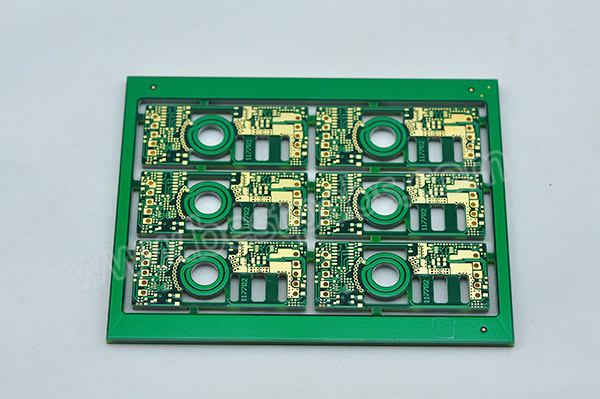
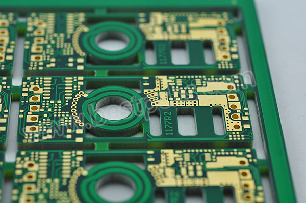
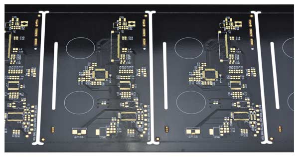
8. EBest Circuit
- Main Business: Custom PCB manufacturing and turnkey PCBA service, including FR4 PCB, HDI PCB, ceramic PCB, metal core PCB, rigid-flex PCB, component sourcing, SMT assembly, testing, and small-batch production.
- Advantages: EBest Circuit is useful when the buyer needs engineering support instead of only an online quote. The team supports DFM pre-review, BOM optimization, PCB manufacturing, component sourcing, PCBA assembly, testing, and project coordination from prototype to production.
- Production Capability: Supports standard FR4 PCB, multilayer PCB, HDI PCB, metal core PCB, ceramic PCB, rigid-flex PCB, component sourcing, SMT assembly, and PCBA testing. Quality systems include ISO9001, ISO13485, IATF16949, AS9100D, REACH, RoHS, and UL-related systems.
- Best Fit: Best for custom PCB/PCBA projects, HDI and special PCB materials, prototype-to-small-batch production, and engineers who want one team to review PCB fabrication and assembly risks together.
How to Choose a Top PCB Manufacturer for Your Project
This section turns the company list into a sourcing decision. Start with the project situation, then choose the supplier type that reduces risk.
1. Simple circuit validation
- Compare JLCPCB, PCBWay, and AdvancedPCB when the board is a simple prototype and the main goal is fast circuit validation. Check board thickness, copper weight, line width, solder mask, surface finish, electrical test, and delivery time.
2. Prototype with SMT assembly
- Compare EBest Circuit, PCBWay, and JLCPCB when the project needs both PCB fabrication and assembly. Check BOM risk, component availability, polarity, connector direction, soldering notes, cleaning requirements, inspection, and packing.
3. HDI, BGA, or compact routing
- Compare Summit Interconnect, TTM Technologies, and EBest Circuit when the board uses fine-pitch BGA, HDI routing, blind/buried vias, resin-filled vias, or controlled impedance. Check stackup review, microvia capability, impedance coupon, EQ communication, and inspection plan.
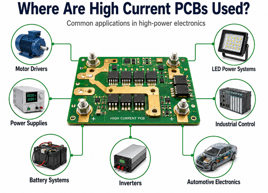
4. LED, power, or thermal product
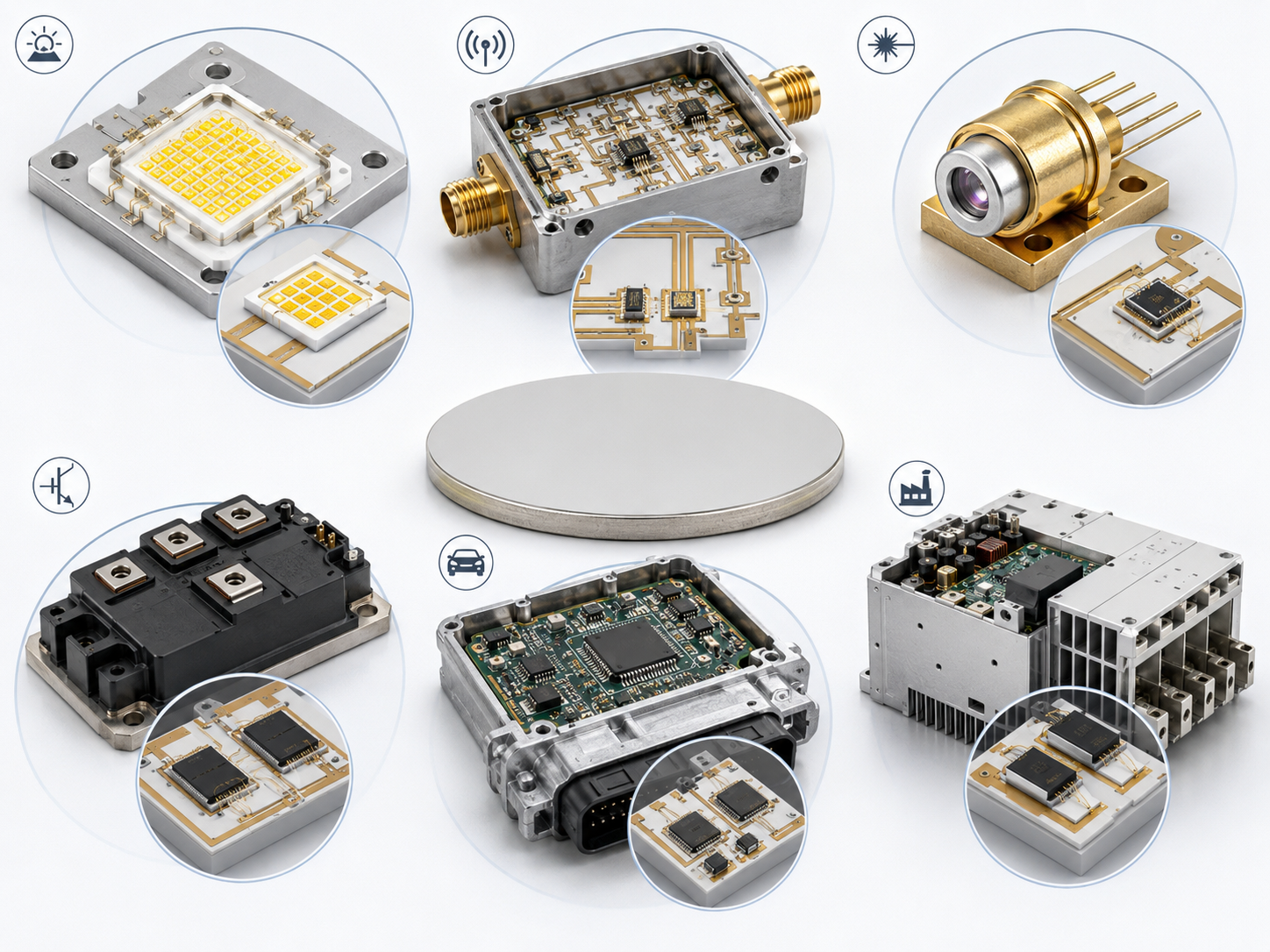
- Choose a manufacturer that understands metal core PCB, copper base PCB, thermal path review, copper thickness, dielectric thermal performance, and assembly reliability. This is where a standard FR4 prototype supplier may not be enough.
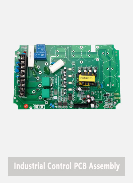
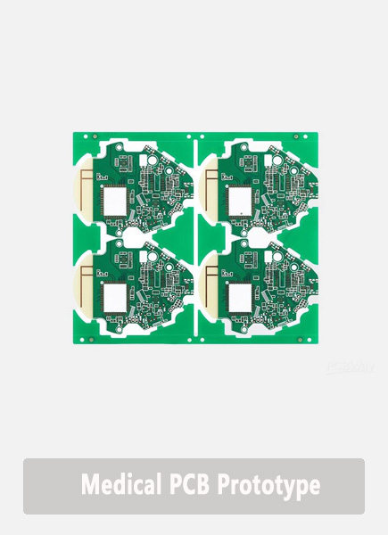
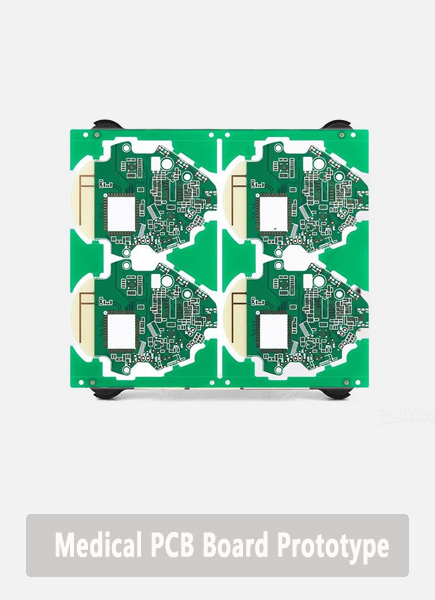
5. Medical, automotive, aerospace, or industrial product
- Compare suppliers with stronger process control and documentation, such as EBest Circuit, Sanmina, and TTM Technologies. Check ISO9001, ISO13485, IATF16949, AS9100D, IPC class, inspection reports, batch traceability, and engineering change control.
6. Prototype moving to small-batch production
- Choose a supplier that can keep engineering details visible from prototype to production. DFM review, BOM review, repeat orders, assembly, testing, cleaning, packing, and production confirmation become more important than the first sample price.
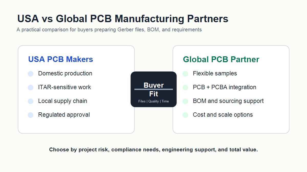
Top PCB Manufacturers in the USA: When Should You Choose Local Supply?
Top PCB manufacturers in the USA are often attractive when buyers need local communication, domestic handling, shorter U.S. logistics, or U.S.-based engineering support. The following examples show different supplier positions in the U.S. market.
1. AdvancedPCB
- Main Business: Standard PCB fabrication, quick-turn prototypes, advanced PCB options, and prototype assembly support.
- Advantages: U.S.-based service, online quoting tools, quick-turn prototype options, DFM-related resources, and standard-to-advanced PCB offerings.
- Production Capability: Suitable for prototype boards, standard FR4 PCBs, selected advanced technology PCBs, flex/rigid-flex options, and assembly-related support depending on project requirements.
- Best Fit: Good reference for U.S. quick-turn prototype jobs and buyers who prefer local PCB handling.
2. TTM Technologies
- Main Business: Advanced PCB manufacturing, RF and specialty components, high-layer-count boards, and larger PCB production programs.
- Advantages: Large manufacturing scale, advanced engineering base, broad market coverage, and stronger fit for complex PCB programs.
- Production Capability: Suitable for complex multilayer boards, advanced materials, high-speed applications, RF-related boards, and production programs that require mature process control.
- Best Fit: Better fit for complex or mature programs than for very small one-off hobby-style prototypes.
3. Summit Interconnect
- Main Business: Complex rigid PCBs, rigid-flex PCBs, HDI, RF/microwave boards, and advanced interconnect projects.
- Advantages: Strong fit for technical boards, impedance control, HDI structures, and projects where engineering communication matters.
- Production Capability: Suitable for high-layer-count boards, HDI, stacked microvias, rigid-flex, and advanced materials depending on the project.
- Best Fit: Good reference for high-density, complex, and advanced PCB projects where process control is more important than the cheapest quote.
4. PCB Unlimited
- Main Business: PCB fabrication, stencils, selected PCB assembly support, and online ordering resources.
- Advantages: Convenient for small businesses, online ordering, stencil service, and prototype support.
- Production Capability: Suitable for standard PCB orders, stencils, metal core PCB options, HDI options, flex/rigid-flex options, and related production support depending on selected service.
- Best Fit: Useful for buyers who want PCB ordering plus related production tools such as stencils.
5. Sanmina
- Main Business: Larger electronics manufacturing, PCB-related support, PCBA, system-level manufacturing, logistics, and repair solutions.
- Advantages: Mature production systems, broader manufacturing resources, and stronger fit for established OEM programs.
- Production Capability: Better suited for larger production programs, assemblies, systems, and supply-chain-heavy projects rather than simple one-off bare PCB orders.
- Best Fit: Good reference for mature products requiring broader electronics manufacturing support.
U.S. supply can make sense when local handling, documentation, or domestic support matters. However, it may not always be the best option for cost-sensitive prototypes, custom PCB/PCBA projects, or small-batch production that needs flexible engineering support.
Top PCB Manufacturers in China for Cost, Speed, and Custom Projects
Top PCB manufacturers in China are widely used by global electronics companies because China has a mature PCB supply chain, material access, SMT capacity, component sourcing networks, and flexible prototype-to-production support.
1. JLCPCB
- Main Business: Online PCB prototype, standard PCB fabrication, simple PCB assembly, and digital ordering.
- Advantages: Fast online quote process, low-cost prototype options, convenient ordering, and strong visibility among engineers and makers.
- Production Capability: Suitable for simple FR4 boards, selected multilayer boards, prototype assembly, and low-complexity sample builds.
- Best Fit: Useful for simple prototypes, fast sample ordering, and low-complexity projects where online convenience matters.
2. PCBWay
- Main Business: PCB prototype, PCB fabrication, PCB assembly, and custom board services.
- Advantages: Broad online PCB service, multiple manufacturing options, prototype and assembly support, and flexible ordering for different board types.
- Production Capability: Suitable for standard prototypes, multilayer PCBs, selected advanced boards, assembly, and custom PCB orders depending on requirements.
- Best Fit: Useful when buyers want online ordering but need more customization than a very basic prototype.
3. EBest Circuit
- Main Business: Custom PCB manufacturing and turnkey PCBA service, including FR4 PCB, HDI PCB, ceramic PCB, metal core PCB, rigid-flex PCB, component sourcing, SMT assembly, and testing.
- Advantages: 20+ years of PCB/PCBA experience, DFM pre-review, BOM optimization support, one-stop PCB manufacturing and assembly, own PCB and PCBA factory, 1,000+ supplier partners, digital traceability, and engineering support from prototype to production.
- Production Capability: Supports standard FR4 PCBs, multilayer PCB, HDI PCB, rigid-flex PCB, metal core PCB, ceramic PCB, component sourcing, PCBA assembly, and testing. Quality systems include ISO9001, ISO13485, IATF16949, AS9100D, REACH, RoHS, and UL-related systems.
- Best Fit: Good fit for engineers who need more than online quoting, especially custom PCB/PCBA projects, medium to large-batch production, special PCB materials, and assembly-related engineering review.
4. Large China PCB factories
- Main Business: High-volume multilayer PCB production, mature board types, and stable repeat orders.
- Advantages: Strong production scale, cost control, and stable output when the product is already mature.
- Production Capability: Suitable for volume multilayer PCBs, repeat production, and standard manufacturing requirements.
- Best Fit: Better for mature products with stable forecasts than for unclear early-stage engineering projects.
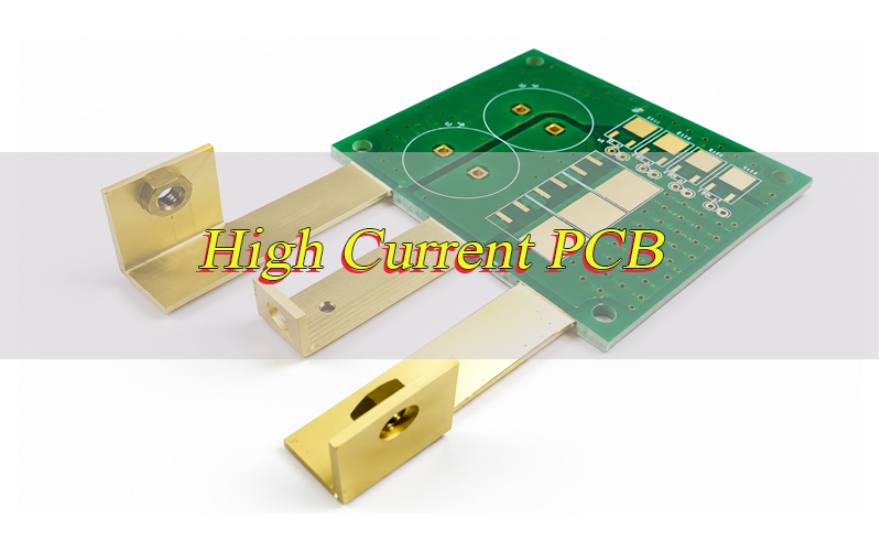
5. Special PCB manufacturers
- Main Business: Ceramic PCB, high-frequency PCB, heavy copper PCB, metal core PCB, and thermal PCB.
- Advantages: More suitable for products with material, heat, RF, insulation, or current-carrying requirements.
- Production Capability: Depends strongly on the factory. Buyers should check material brands, dielectric properties, copper thickness, surface finish, thermal path, and testing requirements.
- Best Fit: Useful for products where a standard FR4 PCB manufacturer cannot meet performance requirements.
The key is to avoid choosing only by price. A low quote is not useful if the supplier misses stackup details, impedance requirements, BOM risks, soldering cleanliness, or test instructions.
Top PCB Manufacturers in the World: What Buyers Should Compare
When people search for top PCB manufacturers in world, they often expect a simple ranked list. But global PCB manufacturing is too diverse for one universal ranking to fit every project.
Large global PCB or EMS programs
- Examples: Sanmina and TTM Technologies. These companies are more relevant for mature production programs, broader manufacturing support, and larger supply chain needs.
Simple prototypes and fast quoting
- Examples: JLCPCB, PCBWay, AdvancedPCB, and PCB Unlimited. These suppliers are easier to compare when the board is simple and the buyer mainly needs fast prototype feedback.
HDI and rigid-flex projects
- Examples: Summit Interconnect, TTM Technologies, and EBest Circuit. These projects need stackup control, via structure review, impedance support, and stronger engineering communication.
Custom PCB and special PCB projects
- Example: EBest Circuit. This category is useful when the project involves FR4 PCB, HDI PCB, ceramic PCB, metal core PCB, rigid-flex PCB, component sourcing, and PCBA assembly.
Turnkey PCB/PCBA projects
- Examples: EBest Circuit, PCBWay, and JLCPCB. The right choice depends on complexity, BOM risk, testing requirements, communication needs, and whether the project will move from prototype to repeat production.
This global comparison should help the buyer choose a supplier type first, then compare companies inside that type.
Top 10 PCB Manufacturers: Why Rankings Are Not Enough
Top 10 PCB manufacturers lists can be useful for market research, but they can also mislead buyers. Many lists mix different supplier types together: bare PCB factories, PCBA assembly companies, online prototype platforms, high-volume global groups, and regional shops.
Before trusting a top 10 list, check how the ranking was created:
- Is it based on revenue?
- Is it based on search visibility?
- Is it based on customer reviews?
- Is it based on factory capability?
- Is it based on a specific country?
- Is it updated for the current year?
- Does it include PCBA or only bare PCB?
If a list does not explain its criteria, treat it as a starting point, not a final sourcing decision.
Prototype shortlist
- Examples: AdvancedPCB, JLCPCB, and PCBWay. Use this group to compare quote speed, prototype convenience, simple board pricing, and basic production capability.
Advanced PCB shortlist
- Examples: Summit Interconnect, TTM Technologies, and EBest Circuit. Use this group when the board involves HDI, rigid-flex, impedance control, fine-pitch routing, or high-layer-count stackups.
Turnkey PCBA shortlist
- Examples: EBest Circuit, PCBWay, and JLCPCB. Use this group when the project needs BOM sourcing, SMT assembly, testing, and packing.
Production shortlist
- Examples: Sanmina, TTM Technologies, and EBest Circuit. Use this group when the buyer needs repeatability, documentation, stable batch control, and a path from prototype to production.
This structure is more useful than a fixed top 10 ranking because it tells the buyer which supplier to contact first for each project stage.
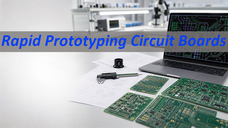
Top Quick-Turn PCB Manufacturers for Prototype and Small-Batch Runs
Top quick-turn PCB manufacturers are valuable when engineers need to validate a design quickly, test a new circuit, build samples for customers, or move a project from drawing to working hardware.
- AdvancedPCB is useful for U.S. quick-turn PCB fabrication, prototype support, and buyers who prefer local handling.
- PCB Unlimited is useful for online PCB ordering, stencils, and small-batch support.
- JLCPCB is useful for low-cost online PCB prototypes and simple assembly flow.
- PCBWay is useful for PCB prototype, assembly ordering, and custom PCB options.
- EBest Circuit is useful for prototype-to-large-batch PCB/PCBA projects where engineering review, DFM feedback, BOM support, and assembly coordination are important.
Quick-turn PCB service is especially important for engineering validation, functional prototypes, sample builds, urgent design revisions, small-batch pilot runs, and pre-production verification.
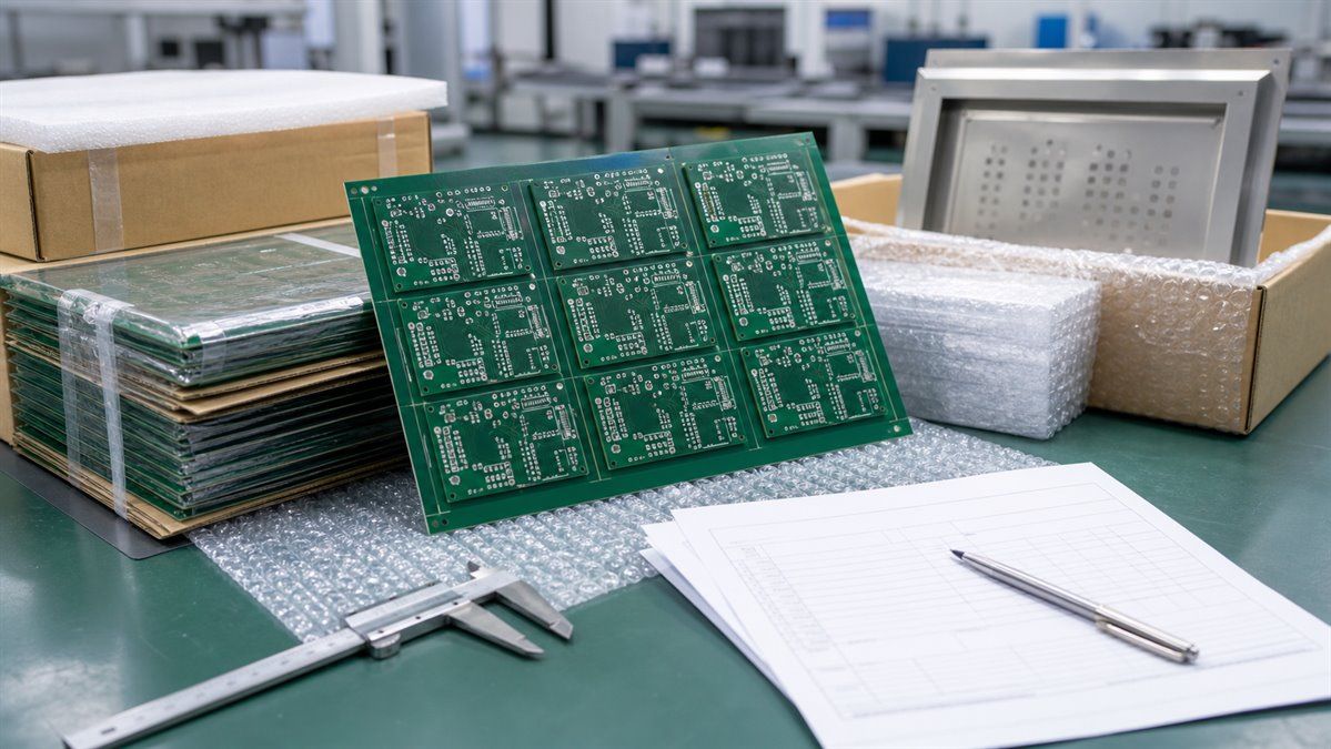
But quick-turn does not mean every PCB can be built instantly. Lead time depends on layer count, material, solder mask, surface finish, controlled impedance, via process, testing, and assembly requirements.
- For example, a standard 2-layer FR4 PCB can usually move faster than a 10-layer HDI PCB with resin-filled vias and impedance control. A bare PCB can also move faster than a full PCBA project that includes BOM review, component sourcing, SMT assembly, cleaning, testing, and packing.
EBest Circuit supports prototype and medium to large-batch PCB/PCBA projects. For urgent projects, our team reviews the files first to confirm whether the lead time is realistic. This avoids promising fast delivery before checking the actual process risk.
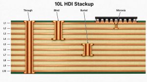
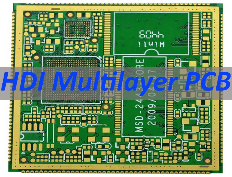
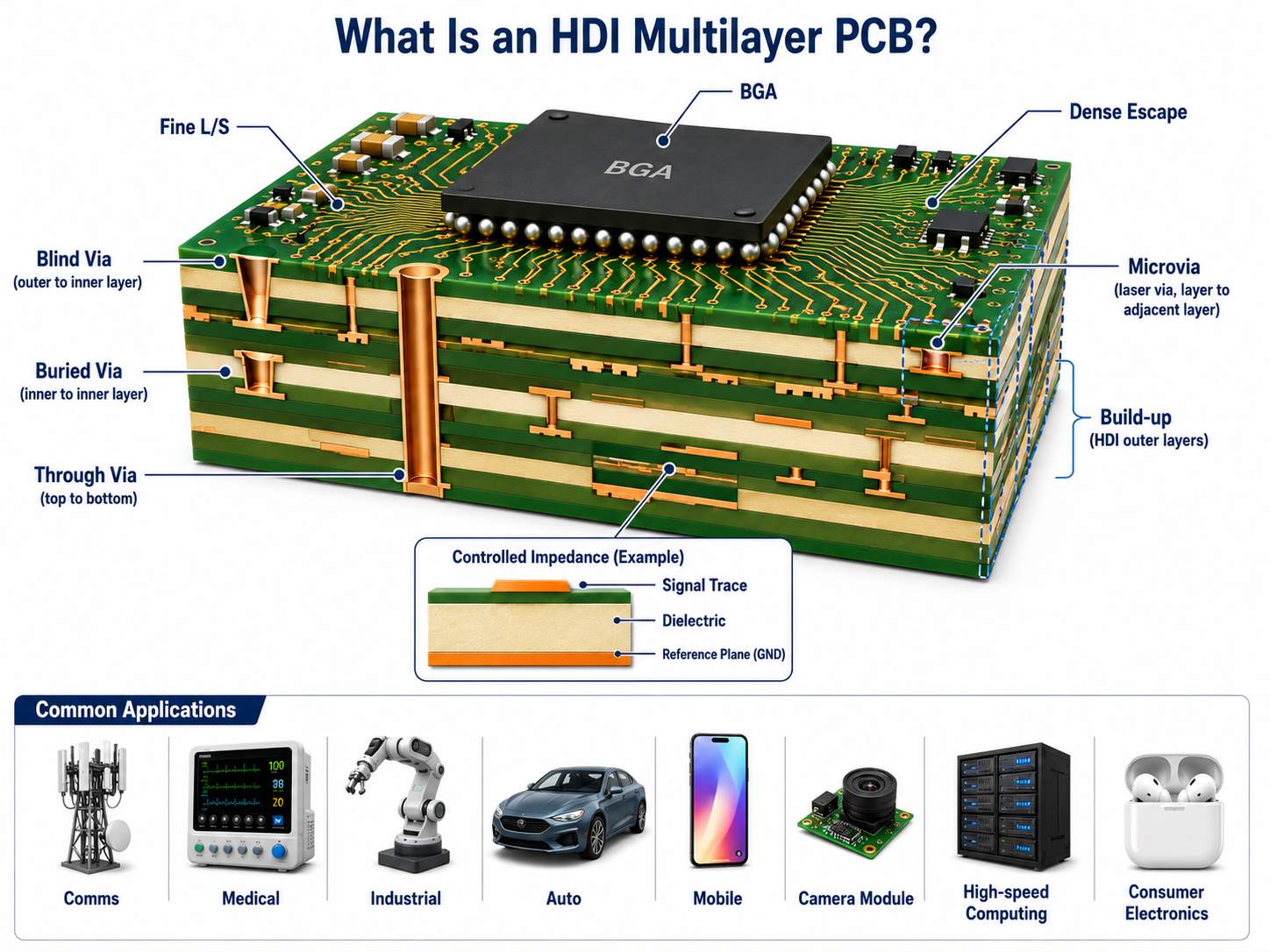
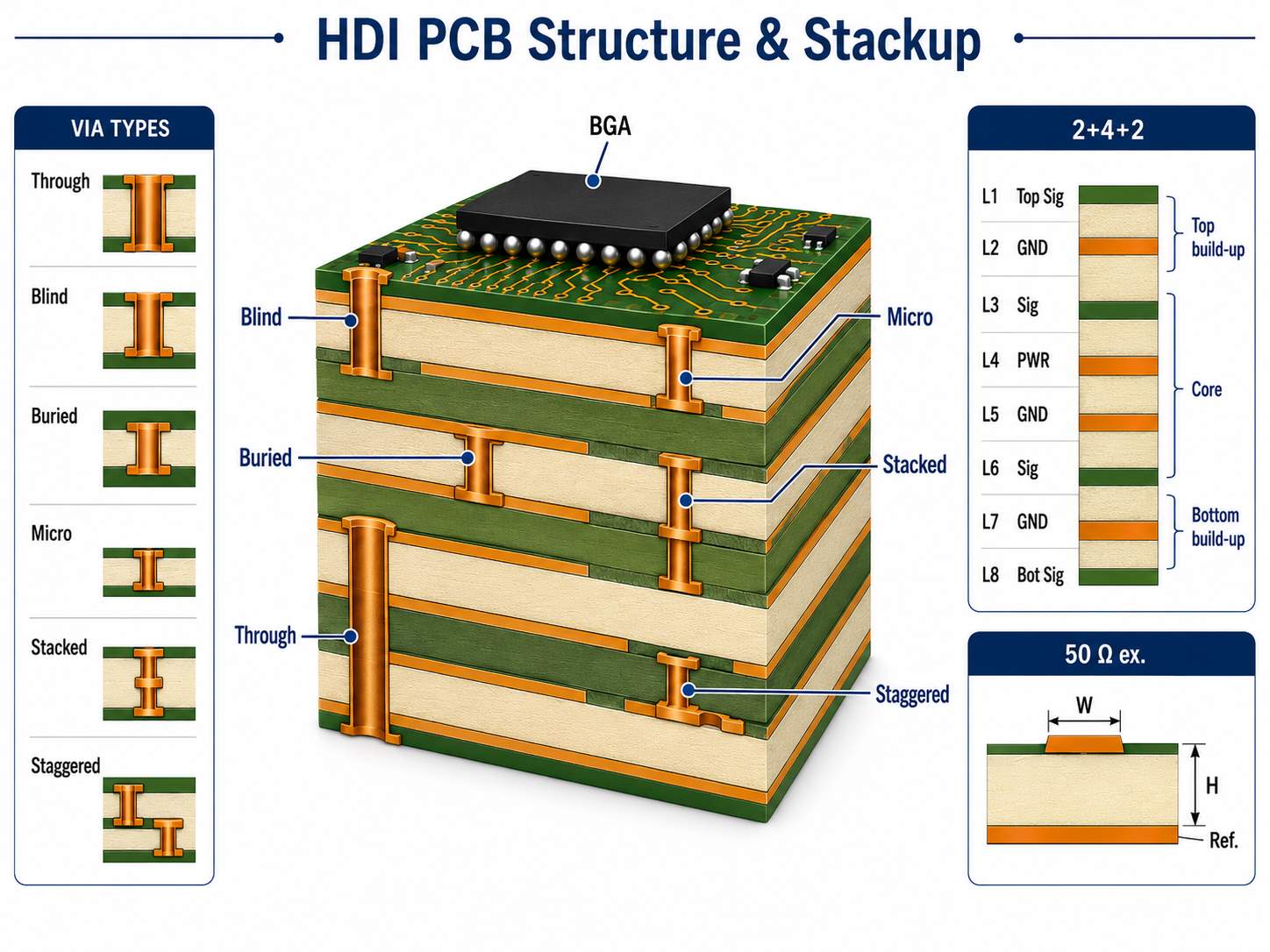
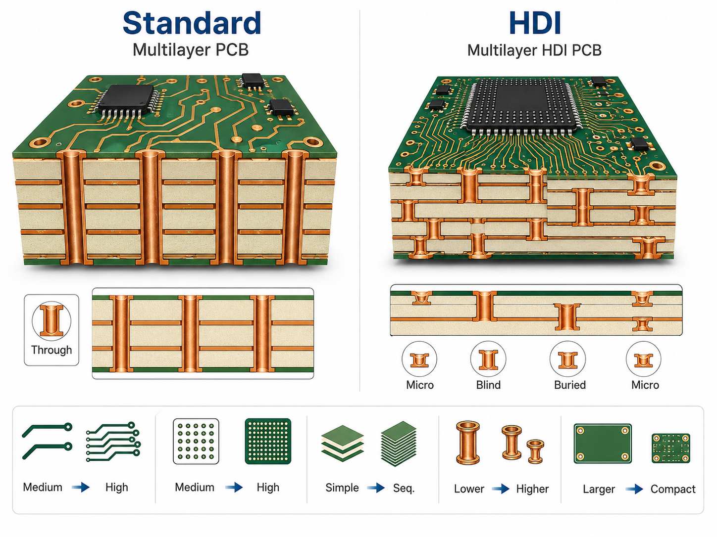
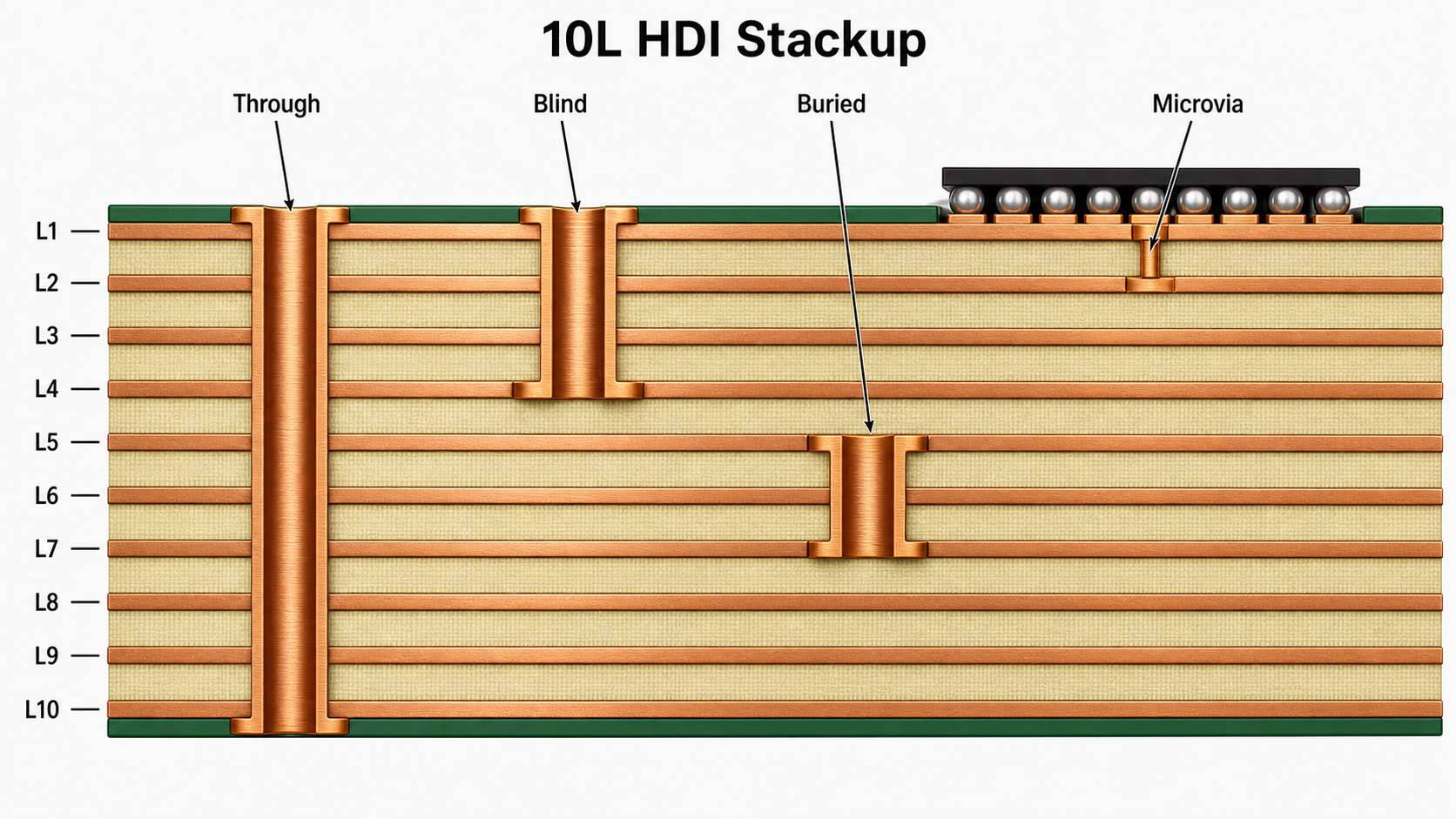
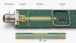
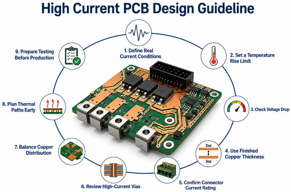
Who Are the Top HDI PCB Manufacturers for High-Density Projects?
For high-density electronics, the best HDI PCB manufacturers are the suppliers that can control stackup, microvias, fine lines, lamination, plating, impedance, and inspection consistently.
- Summit Interconnect is a useful reference for complex PCB, rigid-flex, and HDI interconnect projects.
- TTM Technologies is a useful reference for advanced PCB manufacturing, high-layer-count boards, and complex PCB programs.
- AdvancedPCB is a useful reference for advanced technology PCB options and U.S.-based PCB support.
- EBest Circuit is a useful reference for custom HDI PCB, multi-layer PCB, rigid-flex PCB, controlled impedance review, component sourcing, and turnkey PCBA support.
- PCBWay is a useful reference for selected online HDI prototype and custom PCB projects.
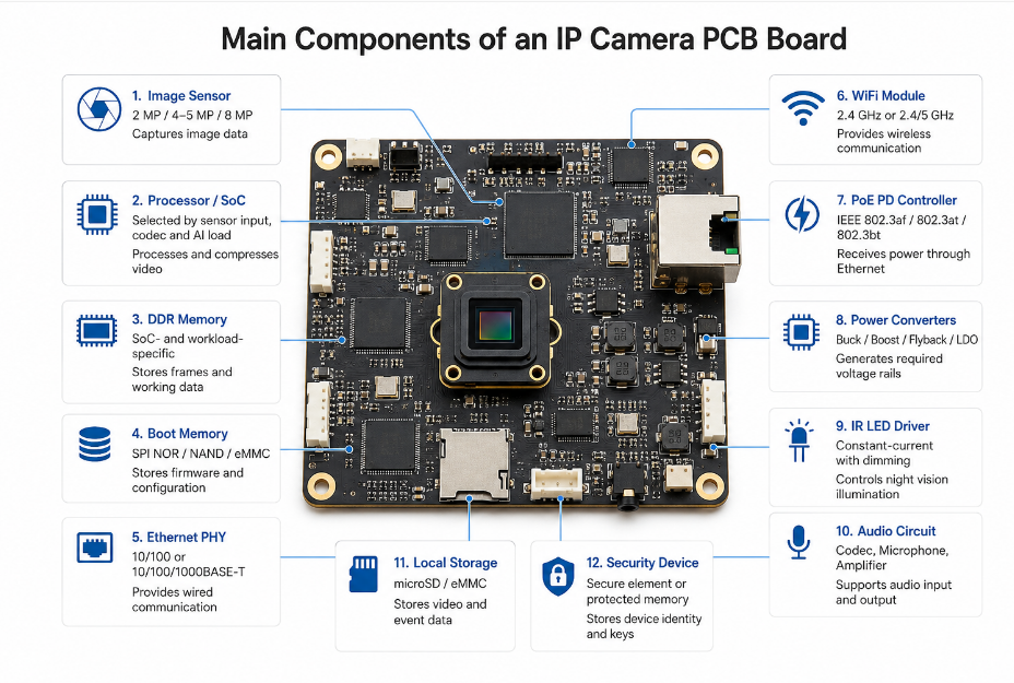
HDI PCB is often used in camera modules, communication devices, medical electronics, industrial control modules, wearable electronics, high-density consumer products, automotive electronics, and compact IoT devices.
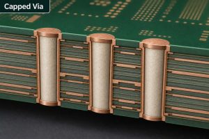
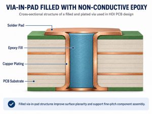
When choosing an HDI PCB manufacturer, buyers should check HDI stackup review, microvia structure, blind and buried vias, resin-filled vias, via-in-pad process, controlled impedance, fine line and spacing, sequential lamination, BGA escape routing, surface finish, and assembly plan.
The related search question “who are the top HDI PCB manufacturers” is useful because HDI projects cannot be judged by price alone. A supplier may be able to make standard multilayer boards but still struggle with HDI reliability, microvia quality, or stackup communication.
For HDI projects, good EQ communication before production is a strong signal. If the manufacturer does not ask questions about stackup, impedance, via process, material, or test requirements, the buyer should be careful.
Top Rated PCB Manufacturers for Automotive, Aerospace, and High-Reliability Electronics
Top rated PCB manufacturers for automotive electronics, aerospace electronics, industrial control, and medical products need stronger process control than ordinary prototype suppliers.
High-reliability PCB projects may involve IPC Class 2 or Class 3 requirements, IATF16949-related quality expectations, AS9100D-related aerospace quality expectations, ISO13485-related medical quality needs, high-temperature materials, controlled impedance, thermal management, long product life cycles, batch traceability, and functional testing.
For these projects, buyers should ask for more than a quotation. They should ask how the supplier handles material control, process confirmation, inspection, test reports, traceability, and engineering changes.
EBest Circuit holds quality-related certifications including ISO9001, ISO13485, IATF16949, AS9100D, REACH, RoHS, and UL-related systems. Our team supports DFM review, BOM optimization, PCB manufacturing, component sourcing, PCBA assembly, and testing. For customers developing high-reliability electronics, this one-stop workflow helps keep engineering details visible from prototype to delivery.
FAQs about Top PCB Manufacturers
Who are the top PCB manufacturers?
The top PCB manufacturers depend on the project. Some suppliers are strong in simple prototypes, some are strong in high-volume production, and others specialize in HDI PCB, rigid-flex PCB, metal core PCB, ceramic PCB, or turnkey PCBA assembly.
How do I choose the best PCB manufacturer?
Choose a PCB manufacturer by matching the supplier to your project stage. A simple prototype may need speed and price, while an HDI board, assembled PCBA, automotive module, or aerospace-related project needs stronger engineering review, quality control, and traceability.
Are top PCB manufacturers in China reliable?
Many China PCB manufacturers are reliable, but quality varies by supplier. Buyers should check process capability, certifications, DFM support, communication quality, inspection standards, and whether the supplier can support both PCB and PCBA if needed.
Should I choose a USA PCB manufacturer or a China PCB manufacturer?
Choose a USA PCB manufacturer when local handling, domestic support, or U.S.-based communication is important. Choose a China PCB manufacturer when you need flexible custom production, cost control, component sourcing, and turnkey PCB assembly support.
What should I ask before ordering from a PCB manufacturer?
Ask about material, stackup, copper thickness, impedance, surface finish, via process, solder mask, panelization, testing, assembly, lead time, and required production reports. For PCBA projects, also confirm BOM sourcing, SMT process, cleaning, inspection, and packing.
All in all, the top PCB manufacturers are not defined only by size, location, or online ranking. A better supplier is the one that understands your board type, process risk, delivery schedule, and product application.
If your project needs custom PCB manufacturing, HDI PCB, rigid-flex PCB, metal core PCB, ceramic PCB, component sourcing, SMT assembly, or turnkey PCBA testing, EBest Circuit (Best Technology) can help review the technical path before production. Send your Gerber files, stackup, BOM, drawings, or project questions to sales@bestpcbs.com. Our engineering team will help you move from prototype to production with clearer technical direction.