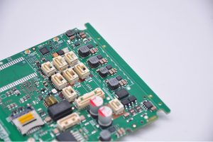
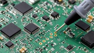
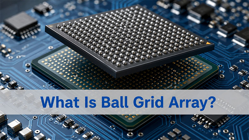
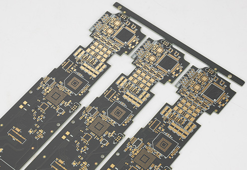
A Ball Grid Array is a surface-mount IC package that uses solder balls on the underside of the component to connect the chip to a printed circuit board. In modern electronics, BGA packaging is widely used because it supports high pin density, compact PCB layouts, better electrical performance, and improved thermal transfer for advanced components such as CPUs, FPGAs, memory chips, and communication ICs.
This guide explains what a Ball Grid Array is, how BGA solder joints are formed, the common types of BGA packages, assembly and inspection challenges, BGA vs. QFP differences, rework methods, and practical PCB design guidelines for reliable BGA routing.
At EBest Circuit (Best Technology), we support customers with PCB fabrication, component sourcing, SMT assembly, BGA soldering, X-ray inspection, functional testing, and engineering DFM review. With experience in high-density PCB and PCBA manufacturing, our team helps engineers identify layout risks, surface finish issues, via-in-pad requirements, soldering concerns, and inspection needs before production starts. This is especially valuable for projects using BGA CPUs, FPGAs, memory devices, industrial controllers, medical electronics, automotive modules, and communication boards. For BGA PCB assembly support or a project review, pls feel free to contact us at sales@bestpcbs.com.
What Is a Ball Grid Array?
A Ball Grid Array, often shortened to BGA, is a surface-mount IC package that uses a grid of solder balls on the bottom side of the component to create electrical and mechanical connections with a printed circuit board.
Instead of using visible leads around the package edge, as seen in QFP or SOP packages, a BGA uses the underside of the chip package. Each solder ball connects to a matching pad on the PCB. During reflow soldering, these solder balls melt, wet the PCB pads, and form solid joints after cooling.
This structure allows a compact component to carry a high number of I/O connections. That is why BGA packaging is widely used in processors, memory devices, FPGAs, communication chips, graphics processors, automotive controllers, and high-performance industrial electronics.
A simple way to understand it is this:
| Package Type | Connection Style | Typical Use |
|---|---|---|
| QFP | Leads around the component edges | Medium pin-count ICs |
| SOP | Gull-wing leads on two sides | Simple ICs and analog parts |
| BGA | Solder balls under the package | High-density and high-speed ICs |
For modern electronics, BGA is no longer a special package. It is common in compact, fast, and high-reliability PCB assemblies.
How Does a Ball Grid Array Work on a PCB?
A BGA package works by connecting the IC to the PCB through solder balls arranged in rows and columns. These balls are placed under the package body. The PCB has matching copper pads, usually finished with ENIG, OSP, immersion silver, or another solderable surface finish.
During assembly, solder paste is printed on the PCB pads by stencil. The BGA component is placed on top of the paste. Then the board passes through a reflow oven.
Inside the oven, the temperature gradually rises. The solder paste activates, the solder balls soften and melt, and the component settles into position through surface tension. After cooling, each solder ball becomes a finished solder joint.
This self-centering behavior is one reason BGA assembly can be stable, even with fine pitch parts. However, the process still depends on accurate stencil design, controlled placement, suitable thermal profiling, and proper inspection.
What Are the Advantages of Ball Grid Array Pack IC?
BGA packages became popular because they solve several problems found in traditional leaded IC packages. They support more connections, better speed, and improved thermal paths in a smaller footprint.
High interconnect density
A BGA uses the entire underside of the package, not only the component edges. This gives engineers more connection points within the same area. A large BGA CPU, FPGA, or processor can have hundreds or even thousands of solder balls.
This is especially useful for advanced circuits where many power, ground, and signal pins must be routed in a compact layout.
Better electrical performance
The solder balls create short connection paths between the IC and PCB. Shorter paths usually mean lower inductance and better signal behavior. This matters in high-speed digital circuits, RF modules, memory interfaces, and communication hardware.
For fast signals, package geometry affects impedance, delay, and noise. BGA packaging helps designers achieve a cleaner connection path than long external leads.
Improved thermal transfer
Many BGA packages offer a better path for heat to move from the chip into the PCB. In some designs, thermal balls, copper planes, and via structures can help move heat away from the device.
This is important for BGA CPU packages, power management ICs, network processors, and other components that generate significant heat during operation.
Smaller footprint
Because connections are placed under the component, the package can be more compact than a leaded package with the same pin count. This is valuable in wearable devices, handheld electronics, automotive control modules, telecom modules, and densely populated PCBA designs.
Good assembly stability
During reflow, molten solder tends to pull the BGA into alignment when the placement offset is within process tolerance. This self-alignment effect helps improve placement results. It does not replace process control, but it gives BGA components a practical advantage in automated SMT assembly.
What Are Common Types of BGA Packaging?
Different BGA packages are designed for different electrical, thermal, mechanical, and cost requirements. The best option depends on the application, operating environment, board density, and reliability target.
| BGA Type | Full Name | Main Feature | Common Applications |
|---|---|---|---|
| PBGA | Plastic Ball Grid Array | Cost-effective organic substrate | Consumer electronics, industrial boards |
| CBGA | Ceramic Ball Grid Array | High thermal and dimensional stability | Aerospace, defense, high-reliability systems |
| FBGA | Fine-Pitch Ball Grid Array | Small pitch and compact size | Mobile devices, memory, compact modules |
| TBGA | Tape Ball Grid Array | Thin package with flexible tape substrate | Thin electronics and special designs |
| FCBGA | Flip-Chip Ball Grid Array | Flip-chip die connection for performance | CPUs, GPUs, ASICs, high-speed processors |
| WLCSP | Wafer-Level Chip Scale Package | Extremely small package close to die size | Smartphones, sensors, compact electronics |
PBGA
PBGA is one of the most common types. It uses a plastic body and an organic laminate substrate. It offers a good balance between cost, availability, and performance. Many microcontrollers, ASICs, communication chips, and general ICs use this package.
CBGA
CBGA uses a ceramic substrate. It has excellent thermal stability and is suitable for demanding environments. Ceramic packages are often selected for aerospace, military, high-temperature, or long-life applications.
FBGA
FBGA has a smaller ball pitch and compact body size. It is often used for memory chips, mobile electronics, and miniaturized products. Because the pitch is smaller, PCB routing and assembly control become more demanding.
FCBGA
FCBGA is used in high-performance chips such as CPUs, GPUs, and advanced processors. The die is flipped and connected directly to the package substrate. This improves electrical and thermal performance, making it suitable for high-speed computing applications.
What Is the BGA Solder Reflow Process?
The BGA solder reflow process is the controlled heating cycle that forms solder joints between the BGA package and the PCB. A reliable result depends on correct paste printing, accurate placement, suitable reflow profile, and post-reflow inspection.
The typical process includes these steps:
1. PCB pad preparation
The PCB pads must be clean, flat, and solderable. Surface finish matters. ENIG is often used for fine-pitch BGA because it provides a flat soldering surface. OSP can also be used, but storage and handling control are important.
2. Solder paste printing
Solder paste is printed onto the PCB pads through a stainless steel stencil. Aperture design, stencil thickness, paste type, and printing pressure all affect paste volume.
Too much paste may cause bridging. Too little paste may cause open joints or weak joints.
3. BGA placement
The pick-and-place machine positions the BGA component onto the printed pads. Since the solder balls are hidden under the package, machine accuracy and package recognition are important.
4. Reflow soldering
The PCB enters the reflow oven. A typical lead-free profile includes preheating, soaking, reflow, and cooling. The exact peak temperature depends on the solder alloy, component rating, board thickness, thermal mass, and manufacturer recommendations.
For many SAC lead-free processes, the peak temperature often falls around 235–250°C. For tin-lead soldering, the temperature is lower. The final profile should always follow the component datasheet and assembly process window.
5. Cooling and solidification
After peak temperature, the solder joints cool and solidify. Controlled cooling helps create stable joint structure and reduce thermal stress.
6. Inspection
Because BGA joints are hidden under the component body, visual inspection is not enough. X-ray inspection is commonly used to check solder joint quality, alignment, voids, bridging, and missing connections.
Why Is Ball Grid Array Inspection More Difficult Than Other SMT Packages?
BGA inspection is more difficult because the solder joints are hidden under the package. With QFP, SOP, or other leaded packages, an operator can inspect leads with optical tools. With BGA, the solder joints are not visible from the outside.
This creates several quality control challenges.
Hidden solder joints
A good-looking component body does not prove that the solder joints underneath are good. A BGA may appear correctly placed while still having opens, shorts, voids, or insufficient solder joints.
Void detection
Voids are air pockets inside solder joints. A small amount of voiding may be acceptable depending on the standard and application, but excessive voiding can reduce thermal and mechanical reliability.
Head-in-pillow defects
Head-in-pillow occurs when the solder ball and solder paste touch but fail to fully merge. This defect can pass basic electrical testing at first and later fail under stress or vibration.
Bridging
Bridging happens when solder connects two adjacent balls. This can create short circuits. Fine-pitch BGAs are more sensitive to this issue.
Open joints
An open joint may occur due to insufficient paste, warpage, poor wetting, contamination, or incorrect thermal profile.
Because of these risks, quality-focused PCBA manufacturers use X-ray inspection for BGA solder joints. For critical products, additional testing such as functional testing, thermal cycling, dye-and-pry analysis, or cross-section analysis may be used.
What Are Common BGA Assembly Defects?
BGA assembly can be reliable when the process is controlled. Most defects come from solder paste variation, component warpage, PCB design issues, moisture sensitivity, or thermal imbalance.
| Defect | What It Means | Common Cause |
|---|---|---|
| Open joint | One or more balls fail to connect | Insufficient paste, warpage, poor wetting |
| Solder bridge | Adjacent balls are connected by solder | Excess paste, poor stencil design, placement offset |
| Void | Air pocket inside the solder joint | Flux outgassing, paste issue, thermal profile |
| Head-in-pillow | Ball and paste do not fully merge | Warpage, oxidation, poor reflow profile |
| Non-wet open | Solder does not wet the pad or ball | Oxidation, contamination, poor surface finish |
| Missing ball | A solder ball is absent or damaged | Component handling or package defect |
| Cracked joint | Joint cracks after stress | CTE mismatch, vibration, thermal cycling |
For high-reliability assemblies, BGA quality should be planned before production. The PCB stackup, pad design, stencil design, reflow profile, handling, moisture control, and inspection method all work together.
BGA vs. QFP: Which PCB Packaging Is Right for Your Project?
BGA and QFP packages are both used for IC assembly, but they suit different design requirements. The right choice depends on pin count, routing density, inspection preference, repair needs, and electrical performance.
| Comparison Item | BGA | QFP |
|---|---|---|
| Connection style | Solder balls under package | Leads around package edges |
| Pin density | High | Medium |
| Footprint efficiency | Excellent | Larger for high pin count |
| Electrical performance | Better for high-speed signals | Good for moderate-speed circuits |
| Inspection | Requires X-ray for solder joints | Easier visual inspection |
| Rework difficulty | Higher | Lower |
| Routing complexity | Higher, especially fine pitch | Easier for low to medium pin count |
| Typical applications | CPUs, FPGAs, memory, processors | MCUs, interface ICs, control circuits |
Choose BGA when your design needs high I/O count, compact size, high-speed performance, or better thermal handling.
Choose QFP when easier inspection, simpler routing, and lower rework complexity are more important than density.
In many real projects, the decision is not purely about cost. It is about the balance between performance, reliability, production capability, and long-term serviceability.
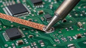
How Are BGA Components Repaired or Reworked?
BGA repair requires specialized equipment because the solder joints are hidden underneath the component. The process is more complex than replacing a leaded IC.
A standard BGA rework process usually includes:
1. Localized heating
A BGA rework station heats the target area with controlled top and bottom heating. This prevents excessive thermal shock and protects nearby components.
2. Component removal
Once the solder joints melt, the defective BGA chip is lifted from the PCB. The operator must avoid pad damage during removal.
3. Pad cleaning
Old solder is removed from the PCB pads. The surface must be flat, clean, and ready for new soldering.
4. Reballing or replacement
If the original component will be reused, it may need reballing. Reballing means placing new solder balls on the package. In many production repair cases, using a new component is safer.
5. Flux application and placement
Flux is applied, and the BGA is aligned on the PCB pads. Accurate positioning is essential.
6. Reflow
The repaired area is heated under a controlled thermal profile. The solder balls melt and form new joints.
7. X-ray and functional testing
After rework, X-ray inspection confirms joint quality. Functional testing confirms electrical performance.
BGA rework should be handled by trained technicians. Excessive heat, poor alignment, or repeated rework can damage the PCB, pads, solder mask, laminate, or nearby components.
What Is BGA Reballing?
BGA reballing is the process of replacing the solder balls on the underside of a BGA component. It is often used when a BGA chip is removed from a PCB and needs to be installed again.
The process usually uses a reballing stencil, solder balls, flux, and controlled heating. The old solder is cleaned from the package pads. New solder balls are aligned and attached to the component.
Reballing may be used in repair work, prototype debugging, chip recovery, or special maintenance projects. However, for high-reliability production, replacing the component with a new part is often preferred.
Reballing quality depends on ball size, pitch accuracy, flux control, surface cleanliness, and heating uniformity.
What Are the Main Design Guidelines for BGA Routing on Multi-layer PCBs?
BGA routing is one of the most important parts of PCB design. A poor fanout strategy can increase layer count, create signal integrity issues, or make fabrication more difficult.
The first step is to review the BGA pitch, ball map, signal groups, power pins, ground pins, high-speed interfaces, and current requirements.
Use the correct land pattern
The pad size should follow the component datasheet and recognized PCB design practices. BGA pads are usually designed as NSMD or SMD pads.
| Pad Type | Meaning | Common Use |
|---|---|---|
| NSMD | Copper pad is smaller than solder mask opening | Often preferred for many BGA designs |
| SMD | Solder mask defines the pad edge | Used in some fine-pitch or special designs |
NSMD pads often provide better solder joint shape and copper definition. SMD pads can improve pad anchoring in certain fine-pitch designs. The final choice depends on package pitch, fabricator capability, and reliability needs.
Plan escape routing early
Escape routing means routing signals from inner BGA balls to other areas of the PCB. For coarse-pitch BGAs, dog-bone fanout may be enough. For fine-pitch BGA packages, via-in-pad or microvia technology may be required.
Use via-in-pad carefully
Via-in-pad can save space and support dense routing. However, the via must usually be filled and capped to prevent solder wicking. If solder flows into an open via, the BGA joint may lose solder volume and become unreliable.
Control impedance for high-speed signals
Many BGA components carry DDR, PCIe, USB, Ethernet, RF, or high-speed serial signals. These traces often need controlled impedance, length matching, reference planes, and careful return paths.
Provide strong power and ground planes
BGA CPU packages, FPGAs, and processors often need many power rails. Use proper plane design, decoupling capacitor placement, and low-inductance power delivery paths.
Place decoupling capacitors close to power pins
Decoupling capacitors should be placed close to the relevant BGA power pins. For dense packages, capacitors may be placed on the opposite side of the PCB when layout allows.
Manage thermal performance
For hot BGA devices, add thermal vias, copper planes, and suitable board stackup design. Thermal simulation may be useful for power-dense electronics.
Match PCB fabrication capability
Fine-pitch BGA routing may require HDI PCB technology, laser microvias, small trace/space, filled vias, and precise registration. Before freezing the layout, confirm the PCB supplier’s capability.
How Does BGA Pitch Affect PCB Manufacturing?
BGA pitch refers to the center-to-center distance between adjacent solder balls. A larger pitch is easier to route and assemble. A smaller pitch supports compact designs but increases manufacturing difficulty.
| BGA Pitch | Routing Difficulty | Typical PCB Requirement |
|---|---|---|
| 1.0 mm | Moderate | Standard multilayer PCB often works |
| 0.8 mm | Moderate to high | Fine trace/space may be needed |
| 0.65 mm | High | HDI may be required |
| 0.5 mm | Very high | Microvias and tight process control |
| 0.4 mm or below | Advanced | HDI stackup and experienced assembly process |
Fine-pitch BGA designs should be reviewed before PCB fabrication. A DFM review can help check pad size, solder mask clearance, via design, escape routing, stencil aperture, and assembly risk.
What Surface Finish Is Suitable for BGA Assembly?
Surface finish affects solderability, pad flatness, shelf life, and assembly quality. For BGA components, flatness is especially important because the solder balls must sit evenly on the PCB pads.
| Surface Finish | Suitability for BGA | Notes |
|---|---|---|
| ENIG | Very common | Flat surface and good solderability |
| ENEPIG | Excellent for demanding applications | Good for wire bonding and high reliability |
| OSP | Common and cost-effective | Requires good storage and handling |
| Immersion Silver | Good solderability | Sensitive to handling and storage |
| HASL | Less preferred for fine-pitch BGA | Surface may be less flat |
ENIG is widely used for BGA assembly because it provides a flat and stable soldering surface. For high-reliability electronics, ENEPIG may be selected when the application requires stronger finish performance.
Why Is Moisture Sensitivity Important for BGA Components?
Many BGA components are moisture-sensitive. If moisture enters the package and the component is heated too quickly during reflow, internal pressure can build up. This may cause package cracking, delamination, or the well-known “popcorn” effect.
To reduce this risk, assembly teams should follow the component’s moisture sensitivity level, also called MSL. This includes dry storage, controlled floor life, baking when required, and proper handling after opening moisture barrier bags.
Moisture control is especially important for expensive BGA CPU packages, FPGAs, memory devices, and automotive-grade ICs.
How to Choose a Reliable PCB Assembly Partner for BGA Components?
BGA assembly is not only about placing a component on a board. It requires process discipline from PCB fabrication to final inspection.
When choosing a PCBA partner for BGA projects, check whether the supplier can support:
- Fine-pitch SMT placement
- Controlled stencil design
- BGA reflow profile development
- X-ray inspection
- BGA rework capability
- HDI PCB fabrication support
- Via-in-pad and filled via process
- Impedance-controlled PCB stackups
- Component moisture control
- Functional testing and traceability
For complex BGA boards, engineering support before production is valuable. A good supplier should review pad design, surface finish, stackup, routing density, test access, and assembly risk before mass production.
EBest Circuit supports PCB fabrication, component sourcing, PCB assembly, X-ray inspection, functional testing, and engineering DFM review for BGA and other high-density SMT assemblies. For projects involving BGA CPU, FPGA, memory, RF modules, or industrial control boards, early design review helps reduce risk before the first build.
In closing, a ball grid array is one of the most important IC package styles in modern electronics. It allows high pin count, compact layout, better electrical performance, and improved thermal paths. These benefits make BGA packaging suitable for CPUs, FPGAs, memory chips, communication ICs, and many other advanced components.
At the same time, BGA assembly requires careful PCB design and strong manufacturing control. The solder joints are hidden, the routing can be dense, and inspection depends heavily on X-ray equipment. For reliable results, engineers should plan the land pattern, fanout, via strategy, surface finish, reflow profile, and inspection method before production.
When BGA design and assembly are handled correctly, it becomes a powerful solution for building smaller, faster, and more reliable electronic products. For BGA PCB assembly, X-ray inspection, or engineering DFM review support, pls feel free to contact EBest Circuit (Best Technology) at sales@bestpcbs.com.
FAQs About Ball Grid Array
What is ball grid array in simple words?
A ball grid array is an IC package that uses solder balls on the bottom side to connect the chip to a PCB. These balls form electrical and mechanical connections during reflow soldering.
What does BGA stand for?
BGA stands for Ball Grid Array. It describes the grid-like arrangement of solder balls under the component package.
What is BGA solder?
BGA solder refers to the solder balls under a BGA package and the solder joints formed between those balls and the PCB pads. In production, solder paste is usually printed on the PCB before reflow.
Why is BGA used for CPUs?
A BGA CPU needs many power, ground, and signal connections in a compact area. BGA packaging supports high pin count, good electrical behavior, and improved thermal transfer, which makes it suitable for processors.
Can BGA components be inspected visually?
Only the outside of the package can be visually inspected. The solder joints are hidden underneath, so X-ray inspection is commonly required for BGA solder joint verification.
Can a BGA chip be repaired?
Yes. A BGA chip can be removed, replaced, or reballed with proper rework equipment. The process requires controlled heating, accurate alignment, pad cleaning, and X-ray inspection after repair.
Is BGA better than QFP?
BGA is better for high-density, high-speed, and compact designs. QFP is easier to inspect and rework. The better choice depends on the project’s electrical, mechanical, cost, and service requirements.
Does BGA require HDI PCB?
Not always. Large-pitch BGA packages may work on standard multilayer PCBs. Fine-pitch BGA components often require HDI technology, microvias, via-in-pad, or tighter trace and space capability.
What causes BGA solder joint failure?
Common causes include poor reflow profile, PCB or package warpage, insufficient solder paste, contamination, excessive voiding, thermal cycling, vibration, and poor pad design.
What is the best PCB surface finish for BGA?
ENIG is commonly used because it provides a flat solderable surface. ENEPIG is also used for demanding applications. OSP can work well when storage and handling are controlled.