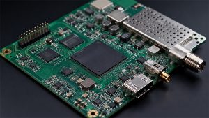
Circuit board test points are designated access locations on a Printed Circuit Board (PCB) that enable engineers and technicians to measure electrical signals, verify functionality, and isolate faults throughout the manufacturing and assembly process. This article covers everything you need to know — from understanding what test points are and how to place them, to leveraging them effectively across the full journey from PCB fabrication to PCBA test.
Are your test points costing you time and yield instead of saving them?
Here are five pain points engineers commonly face with circuit board test points:
- Test point locations conflict with components or heatsinks, making probing physically impossible.
- Inconsistent probe contact causes floating or inaccurate voltage readings during ICT.
- High-density SMD layouts leave no room for standard through-hole test points.
- Automated bed-of-nails fixtures fail due to poor pad geometry or incorrect pitch on SMD test points.
- Insufficient test coverage on critical nets leads to escaped defects that only surface in the field.
As a professional PCBA manufacturer, we tackle these issues head-on:
- DFM pre-screening ensures test points on a circuit board are placed in accessible, probe-friendly zones.
- High-quality pad materials and controlled-impedance design minimize resistance and signal distortion.
- SMD test point recommendations are tailored to your board density and height constraints.
- Pad geometry is optimized for compatibility with standard compact probe tip circuit board test points.
- Full net coverage analysis guarantees all critical signals — power, ground, clocks — have dedicated test points.
EBest Circuit (Best Technology) is a one-stop PCB and PCBA manufacturer with 20+ years of industry experience, serving 1,800+ clients and 10,000+ engineers worldwide. Our in-house factory, 1,000+ supply chain partners, and ISO 9001/13485, IATF 16949, and AS9100D certifications ensure precision from bare board to finished assembly. With a 20-year experienced engineering team offering DFM analysis, BOM optimization, and process adaptation advice, we deliver PCBA in as fast as 1.5 weeks. For inquiries, pls feel free to contact us at sales@bestpcbs.com.

What Are Circuit Board Test Points?
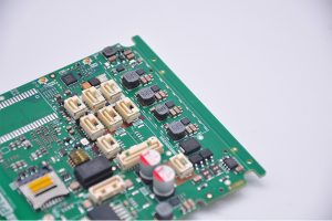
Circuit board test points are small, exposed metal pads, vias, or mechanical pins placed on a PCB to provide safe, repeatable access for test equipment. Think of them as the “nerve endings” of your board — each one giving a diagnostic window into what is happening electrically at that exact location, without requiring you to probe fragile IC legs or lift solder joints.
From the earliest stage of PCB fabrication through to PCBA functional testing, printed circuit board test points appear in several physical forms:
| Type | Construction | Typical Use Case |
|---|---|---|
| Solder Pad (SMD) | Flat copper pad, no through-hole | High-density, low-profile boards |
| Through-Hole Via | Plated hole exposed on both sides | Manual probing, dual-sided access |
| Mechanical Pin (Keystone) | Press-fit or soldered pin | Repeated manual probing, durability |
| Testpad on Ground Plane | Large copper island | Reference ground for oscilloscope probes |
Each test point circuit board design targets a specific combination of probe compatibility, board density, and test frequency. The golden rule is simple: a test point that cannot be reached by a probe is no test point at all.
Electrically, test points act as low-impedance windows onto signal nets. When correctly designed, they introduce negligible loading — typically less than 1 pF of parasitic capacitance on a well-laid-out SMD pad — preserving signal integrity for measurements on high-speed nets. Poorly designed pads, however, can act as stubs that distort waveforms, especially above 100 MHz.
In short, circuit board test points are the foundation of any robust In-Circuit Test (ICT) or Functional Circuit Test (FCT) strategy, and their quality directly determines how efficiently a board can move from fabrication to verified, shippable product.

What Are Keystone Test Points In PCB Design?
Keystone test points refer to a family of small, mechanically robust test hardware — most commonly press-fit or soldered pins — originally manufactured by Keystone Electronics and now widely replicated across the industry. Unlike a simple copper pad, a Keystone-style test point is a physical component that stands proud of the board surface, giving a probe tip a clearly defined and durable landing zone.
Keystone test points are typically available in the following configurations:
- Thru-hole pins: Pressed or soldered into a plated through-hole; extremely robust for high-cycle manual probing environments.
- Surface-mount loop or pad variants: Low-profile options for boards with height restrictions, retaining mechanical durability while reducing z-axis space.
- Color-coded versions: Red (positive/signal), black (ground), white (neutral) — essential for quick identification during manual debugging.
- Miniature SMD versions: For fine-pitch, high-density designs where even a standard 1 mm pad may be too large.
The mechanical advantage of a Keystone-style component over a bare pad becomes especially apparent in manufacturing environments where the same board is probed hundreds or thousands of times during ICT. A bare copper pad can oxidize, deform under repeated contact, or delaminate from the substrate. A properly installed Keystone pin resists all three failure modes.
From a PCB design perspective, integrating these components requires a dedicated footprint with sufficient keep-out clearance so that neighboring components do not obstruct probe access. Most designers allocate a 1.0–1.5 mm clearance radius around each pin, confirmed during DFM review before fabrication begins.
In summary, Keystone test points bridge the gap between a fragile solder pad and a bulky connector — delivering the mechanical reliability of a connector with the PCB footprint of a test pad.
Why Are PCB Test Points Important In Assembly?
PCB test points are the quality gatekeepers of the PCBA process. Without them, a finished board is essentially a black box — you can power it on and observe behavior, but you cannot pinpoint where a fault originates. With them, every critical net becomes observable, and every manufacturing defect becomes traceable.
The impact is measurable across multiple dimensions of production:
| Aspect | Without Test Points | With Test Points |
|---|---|---|
| Fault Isolation | Hours of blind signal tracing | Minutes with direct probe access |
| ICT Compatibility | Bed-of-nails fixture impossible | Full automated ICT enabled |
| Signal Integrity Risk | High — probing IC pins risks damage | Low — isolated pad absorbs probe force |
| First-Pass Yield | Lower — defects escape to FCT or field | Higher — shorts and opens caught early |
| Rework Cost | High — faults found late cost more to fix | Low — defects caught at source |
During SMT assembly, the most common defect categories — solder bridges, cold joints, missing components, and reversed polarities — are all detectable through properly placed test points on a circuit board. An ICT system using a bed-of-nails fixture can test hundreds of nets in under 10 seconds, but only if each net has a dedicated, accessible test point.
Beyond ICT, PCB test points also support:
- In-System Programming (ISP): JTAG and SWD test points allow firmware flashing directly on the production line.
- Boundary Scan Testing: IEEE 1149.1-compliant test point clusters enable digital chain testing of complex ICs.
- Burn-in Monitoring: Test points on power rails allow continuous voltage and current monitoring during thermal stress testing.
The ROI of good test point design is straightforward: early defect detection at the ICT stage costs a fraction of the rework or warranty cost incurred when a defect escapes to the customer. For high-volume production runs, a 1% improvement in first-pass yield can translate directly into tens of thousands of dollars in savings per quarter.
Where Are The Test Points On A Circuit Board?
Knowing where test points on a circuit board are located — and why — is as important as knowing what they are. Placement is not arbitrary; it follows a set of design principles that balance electrical accessibility, physical reachability, and automated test fixture compatibility.
Primary placement zones include:
- Board edges and corner areas — Low component density in these zones makes probe access straightforward and reduces fixture complexity.
- Near power regulators and DC-DC converters — Voltage rails must be verified at the output of every regulation stage.
- Adjacent to microcontrollers and FPGAs — Clock lines, reset signals, and communication buses (I²C, SPI, UART) all benefit from dedicated test points.
- On crystal oscillator outputs — Frequency verification requires a clean, low-capacitance measurement point close to the source.
- On all power and ground nets — A solid ground reference test point within 20 mm of every signal test point is best practice for oscilloscope probing.
- On high-current traces — Current-sense resistor terminals with dedicated test points allow in-circuit current measurement without breaking the circuit.
Placement rules to follow:
- Never position a test point underneath a heatsink, shield can, or tall electrolytic capacitor.
- Maintain a minimum of 1.0 mm clearance between adjacent test points on ICT fixtures to prevent probe cross-contact.
- For double-sided ICT, mirror critical test points on both top and bottom layers to allow a two-sided fixture.
- Keep test point pitch ≥ 2.54 mm (100 mil) for standard bed-of-nails probes; for fine-pitch ICT, 1.27 mm (50 mil) is achievable with precision fixtures.
During DFM analysis, our engineers review Gerber files specifically to confirm that all test points on circuit board layouts are reachable, correctly sized, and free of solder mask obstruction. An exposed, soldermask-free copper pad is the baseline requirement — any mask coverage over a test point renders it unreliable.
How To Use Test Points On A Circuit Board?
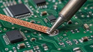
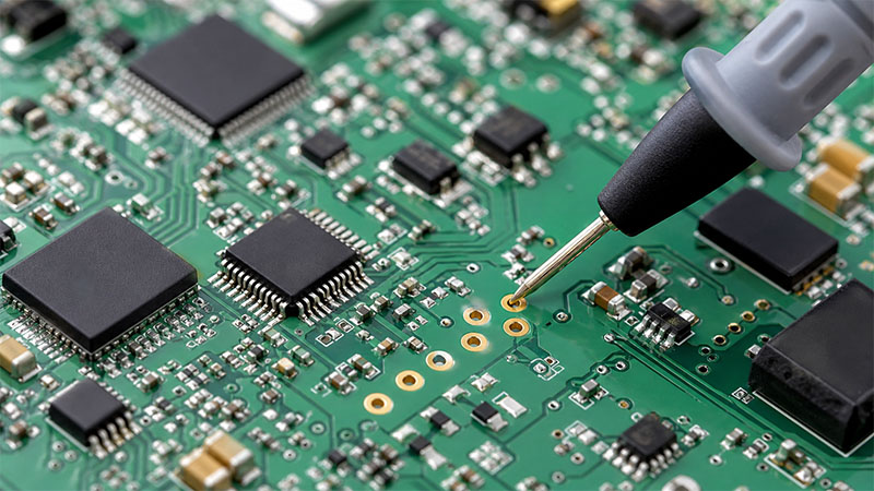
Understanding how to use test points on a circuit board correctly is essential for obtaining reliable measurements and avoiding board damage. The process is straightforward, but each step matters.
Step-by-step guide to probing test points:
- Identify the test point using the schematic or PCB layout file. Cross-reference the reference designator (e.g., TP1, TP_GND) with the net it monitors. Do not guess — probing the wrong net can give misleading data or cause a short.
- Select the right probe tip. For SMD pads smaller than 1 mm, use a fine-tipped probe (0.5 mm diameter or less). For through-hole or Keystone pins, a standard 1 mm hook probe works well. Compact probe tip circuit board test points require matched probe geometry for consistent contact.
- Set up your instrument correctly. To measure ar test points on a circuit board for volts, confirm whether the net is DC or AC, then set your multimeter or oscilloscope to the appropriate range and coupling. For power rails, DC voltage mode is standard. For clock or data lines, use AC coupling with the correct oscilloscope bandwidth.
- Make contact gently but firmly. Place the probe perpendicular to the pad surface. Avoid dragging the tip across the board, which can dislodge nearby 0201 or 0402 components. For oscilloscope measurements, always connect the ground clip to the nearest ground test point — not to a remote chassis ground — to minimize loop inductance.
- Read and record the measurement. Compare against the expected value from the design specification. Flag any deviation exceeding ±5% on power rails or unexpected waveform distortion on signal nets.
- Do not apply excessive force. SMD test pads are bonded to the PCB substrate through copper traces and soldermask. Repeated heavy probing can delaminate the pad, especially on thin (0.8 mm) boards.
Quick reference for common measurements:
| Measurement | Instrument | Mode | Reference Point |
|---|---|---|---|
| DC power rail voltage | Multimeter | DC Voltage | GND test point |
| Clock frequency | Oscilloscope | AC, 10× probe | Nearest GND |
| I²C signal integrity | Oscilloscope | AC, 1× probe | GND test point |
| In-circuit resistance | Multimeter | Resistance (power OFF) | N/A |
Following this process consistently makes test points on a circuit board a genuinely powerful diagnostic tool rather than a source of measurement error.
When Should You Use An SMD Test Point?
An SMD test point is the default choice for the vast majority of modern PCB designs. As board complexity has increased and component pitch has shrunk, through-hole test points have become the exception rather than the rule. Understanding when to specify an SMD test point — and which variant to choose — directly affects your testability, board density, and manufacturing cost.
Use an SMD test point when:
- The board uses double-sided SMT assembly. Through-hole pins require wave soldering or hand soldering, which adds process steps. SMD variants are reflowed with the rest of the components.
- Height clearance is restricted. In flat consumer electronics or wearables, even a 1 mm tall Keystone pin may exceed the allowable z-axis envelope. An SMD pad adds zero height.
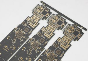
- The board density is high. On a 6-layer or 8-layer HDI board with 0201 passives, the footprint of a through-hole test point competes directly with signal routing. An SMD pad (typically 0.8 mm × 1.2 mm) integrates without displacing any traces.
- Automated ICT is planned. Bed-of-nails fixtures are designed around consistent SMD pad locations, which are photolithographically defined and highly repeatable in position.
- The test point will be probed infrequently. For production-line ICT, SMD pads survive thousands of probe contacts with minimal wear. For daily manual probing in a lab setting, a Keystone pin offers better longevity.
SMD test point pad sizing guidelines:
| Board Pitch Environment | Recommended Pad Diameter | Solder Mask Opening |
|---|---|---|
| Standard (≥ 0.5 mm pitch) | 1.0 mm | 1.2 mm |
| Fine-pitch (0.3–0.5 mm) | 0.7 mm | 0.9 mm |
| Ultra-fine / HDI | 0.5 mm | 0.65 mm |
One important design note: SMD test points should always be placed on the solder mask layer with an explicit opening (NSMD — non-solder mask defined) to ensure the copper pad is fully exposed and oxidation-free when the board arrives at the ICT station. A test point buried under solder mask is electrically invisible to a probe.
How Do Probe Tip Circuit Board Test Points Improve Testing?
The physical interface between a probe tip and a PCB test point is where theory meets reality. Even a perfectly designed test point becomes unreliable if the probe tip is mismatched in geometry, spring force, or material. Probe tip circuit board test points — the combined system of pad and probe — must be engineered together, not independently.
Why probe-pad compatibility matters:
A standard ICT bed-of-nails probe tip exerts between 50 g and 150 g of force on each test point. If the pad diameter is smaller than the probe tip contact area, the probe can slip, bridge to an adjacent trace, or fail to make reliable ohmic contact. The result is false failures on a good board — one of the most expensive problems in PCBA production, because it drives unnecessary rework.
Key parameters of the probe-pad interface:
| Parameter | Effect on Test Reliability |
|---|---|
| Probe tip diameter vs. pad diameter | Must be ≤ pad diameter; mismatch causes slippage |
| Spring force | Too low → intermittent contact; too high → pad delamination |
| Tip material (beryllium copper vs. tungsten) | Tungsten for hard surfaces; BeCu for gold-plated pads |
| Contact resistance | Target < 10 mΩ; higher values introduce voltage offset errors |
| Probe pitch | Minimum 2.54 mm for standard fixtures; 1.27 mm for fine-pitch |
Compact probe tip circuit board test points — a combination of miniaturized pads (≤ 0.8 mm) paired with precision fine-tipped probes — are used specifically in high-density designs where standard fixtures cannot achieve the required test coverage. These systems are more expensive but essential for complex boards where testability cannot be sacrificed for density.
Benefits across the production lifecycle:
- ICT stage: Consistent probe contact yields repeatable resistance and capacitance measurements, enabling accurate solder joint quality verification.
- FCT stage: Oscilloscope probes with fine tips can access high-speed signal test points (e.g., USB 3.0, MIPI) without adding the capacitive loading of a large hook probe.
- Field debugging: A well-designed probe tip and pad system allows field service engineers to diagnose board failures in-system without removing the PCB from the enclosure.
The takeaway is clear: specifying probe tip circuit board test points as a matched system — not as separate pad and probe decisions — is what separates a testable, manufacturable design from one that struggles at every quality gate.
How Can EBest Circuit (Best Technology) Support Circuit Board Test Points From PCB Fabrication To PCBA Test?
Supporting circuit board test points throughout the full production lifecycle — from the first Gerber review to the final functional test — requires more than equipment. It requires process integration, engineering expertise, and quality infrastructure that spans every stage. EBest Circuit (Best Technology) provides exactly that.
Our end-to-end support process:
1. DFM Analysis and Test Point Review Before a single panel is fabricated, our 20-year experienced PCB/PCBA engineers review your Gerber files and test point placement. We flag inaccessible pads, undersized openings, incorrect pitch, and nets missing test coverage. You receive a written DFM report with actionable recommendations — not just a pass/fail verdict.
2. BOM Optimization for Test Components If your design specifies Keystone test points or specific SMD test point components, our procurement team cross-references your BOM against our 1,000+ supply chain partners to source the correct parts at competitive cost. We flag obsolete or long-lead-time test point components before they delay your build.
3. Precision SMT Assembly Our automated SMT lines place SMD test points with the same accuracy as any other 0402 or fine-pitch component — typically ±0.05 mm placement accuracy. Correct placement ensures every pad aligns with your ICT fixture, eliminating the most common cause of bed-of-nails fixture failures.
4. In-Circuit Test (ICT) and Functional Circuit Test (FCT) We operate advanced ICT systems compatible with industry-standard probe tip sizes, from 100-mil standard probes to 50-mil fine-pitch probes for high-density boards. Our FCT stations are configured to your test plan, verifying functional performance at every critical test point.
5. Traceability Through Digital Manufacturing Our digital workshop enables material and batch tracking within 5 seconds. Every board that passes through our line is traceable — which means if a test point defect pattern emerges on a specific batch, we can isolate the root cause rapidly and prevent further escapes.
6. Fast Delivery — 1.5-Week PCBA Turnaround From board fabrication through component assembly and testing, we offer 1.5-week PCBA delivery for qualifying projects. Our integrated PCB + PCBA factory eliminates hand-off delays between fabrication and assembly, keeping your development and production schedules on track.
Whether you are prototyping a new design and need sample quantities with full ICT coverage, or scaling to mass production and require consistent test point quality across thousands of units, EBest Circuit (Best Technology) provides the engineering depth and manufacturing capacity to support you.
If any questions, pls feel free to contact us anytime via sales@bestpcbs.com.
In conclusion, circuit board test points are far more than convenient probe locations — they are the structural backbone of a reliable, testable, and manufacturable PCB design. From the first placement decision during PCB fabrication through every ICT and FCT station on the PCBA line, well-designed printed circuit board test points determine how quickly defects are caught, how accurately signals are measured, and how confidently a finished product can be released.
Throughout this guide, we have covered the full landscape: from understanding what SMD test points and Keystone test points are, to knowing exactly where to place test points on a circuit board, how to use them correctly, and how to match probe tip circuit board test points for maximum measurement reliability. Each element is interconnected — a gap at any stage undermines the entire test strategy.
At EBest Circuit (Best Technology), we bring 20 years of PCB and PCBA manufacturing expertise to every project that involves circuit board test points. Our integrated factory, experienced engineering team, and ISO/IATF/AS9100D-certified quality systems ensure that your test point strategy is validated during DFM, executed precisely during assembly, and verified rigorously during testing — all within a 1.5-week PCBA delivery window. Ready to build a board that tests as well as it performs? Pls feel free to reach out to our team at any time via sales@bestpcbs.com.
FAQs About Circuit Board Test Points
Q: What does “N F” mean on a circuit board test point?
A: “N F” stands for “No Fill,” indicating that the via or pad should be left open — not filled with solder, epoxy, or solder mask. This keeps the test point exposed and accessible for probing. You will commonly see “NF” or “DNF” (Do Not Fill) in assembly drawings and BOM notes for test vias.
Q: How many test points are enough for a PCB design?
A: There is no universal number, but a practical rule is: every critical net needs at least one test point. At minimum, this includes all power supply rails, all ground nets, all clock signals, all reset lines, and all major communication interfaces (SPI, I²C, UART, USB, CAN). For high-reliability applications — medical, aerospace, automotive — 100% net coverage is the target. For consumer electronics, 60–80% coverage of critical nets is a common baseline.
Q: Can test points be used for programming as well as testing?
A: Yes. JTAG and SWD interfaces are routinely exposed through dedicated test points rather than connectors in production designs. This allows in-system programming (ISP) during the PCBA test stage without adding a bulky connector to the bill of materials. The test point footprints for programming are typically clustered together and labeled clearly on the silkscreen.
Q: What is the minimum pad size for an SMD test point on an ICT fixture?
A: For standard 100-mil (2.54 mm) pitch ICT probes, a 1.0 mm diameter exposed copper pad is the practical minimum. For fine-pitch fixtures at 50-mil (1.27 mm) pitch, 0.6–0.7 mm pads are achievable with precision probes. Always confirm the minimum pad size with your ICT fixture vendor before finalizing the PCB layout.
Q: Should test points be on the top side, bottom side, or both?
A: For single-sided ICT, placing all test points on one side (typically the bottom) simplifies fixture design. For double-sided ICT or very high net coverage requirements, test points on both sides are acceptable but require a more complex two-sided fixture. During DFM review, our engineers will recommend the optimal distribution based on your board stack-up and test strategy.