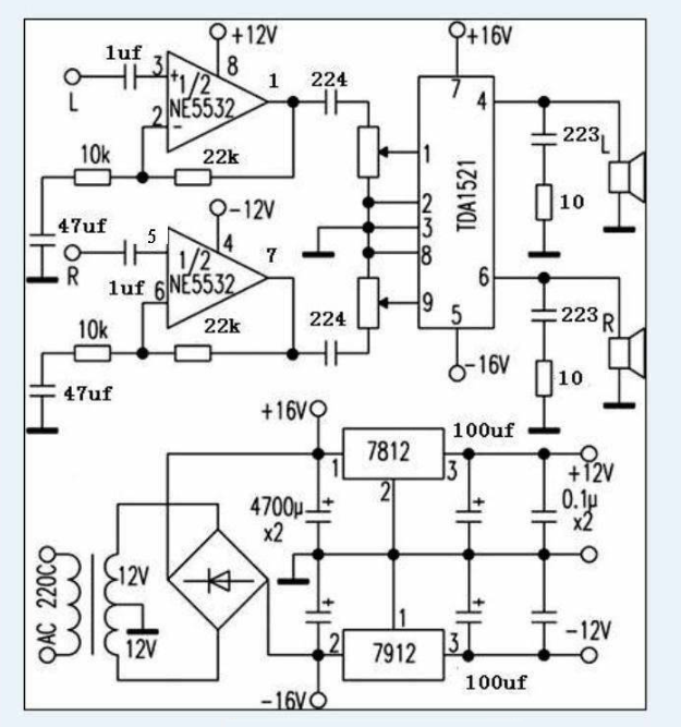
PCB Line Width and Flow Current Comparison Table
In PCB manufacturing, the term of “OZ” always refers to copper thickness, 1OZ thickness means evenly spread 1OZ copper foil on the 1 square foot areas, and this thickness is around 0.035mm. So, 35um, 50um, 70um correspond to 1OZ, 1.5OZ, 2OZ.
The full name of OZ is ounce, it is the weight per unit area to express the thickness of the copper foil, the format is: 1OZ=28.35g/FT2
PCB Line Width and Flow Current Comparison Table Chart
| PCB Line Width and Flow Current Comparison Table Chart | |||||
| Line width (mm) | Current (A) | Line width (mm) | Current (A) | Line width (mm) | Current (A) |
| 0.15 | 0.2 | 0.15 | 0.5 | 0.15 | 0.7 |
| 0.2 | 0.55 | 0.2 | 0.7 | 0.2 | 0.9 |
| 0.3 | 0.8 | 0.3 | 1.1 | 0.3 | 1.3 |
| 0.4 | 1.1 | 0.1 | 1.35 | 0.4 | 1.7 |
| 0.5 | 1.35 | 0.5 | 1.7 | 0.5 | 2.0 |
| 0.6 | 1.6 | 0.6 | 1.9 | 0.6 | 2.3 |
| 0.8 | 2.0 | 0.8 | 2.4 | 0.8 | 2.8 |
| 1.0 | 2.3 | 1.0 | 2.6 | 1.0 | 3.2 |
| 1.2 | 2.7 | 1.2 | 3.0 | 1.2 | 3.6 |
| 1.5 | 3.2 | 1.5 | 3.5 | 1.5 | 4.2 |
| 2.0 | 4.0 | 2.0 | 4.3 | 2.0 | 5.1 |
| 2.5 | 4.5 | 2.5 | 5.1 | 2.5 | 6.0 |
| Copper thickness 1OZ (0.035mm) | Copper thickness 1.5OZ (0.05mm) | Copper thickness 2OZ (0.7mm) | |||
From the chart as above:
35um copper thickness and 0.4mm line width, the current is 1.1A;
50um copper thickness and 0.4mm line width, the current is 1.35A;
70um copper thickness and 0.4mm line width, the current is 1.7A.
EBest Circuit (Best Technology) PCB Line Width and Flow Current Calculator
When using copper foil as a conductor for large currents, the width of the copper foil should be selected by reducing the current-carrying capacity values from the reference table by 50%. However, there are other methods to address this. In some power circuits, due to PCB constraints, the current-carrying paths are designed as long pads, and solder is added on top of them to form a thick current path. Besides adding tin to the copper foil to increase the current capacity, you can also consider using multiple PCB layers to increase the current. For instance, placing the same circuit on both the top and bottom layers or using short jumper wires can also help increase the current capacity.
How Wide Should the Trace be If Current is 1A?
1. Due to the limited thickness of the copper foil on the copper-clad board, the current-carrying capacity of the copper foil needs to be considered for strip-shaped copper foil that needs to carry a large current. Taking the typical thickness of 0.03mm as an example, if the copper foil is used as a strip-shaped conductor with a width of W (mm) and a length of L (mm), its resistance is 0.0005 L / W ohms. Additionally, the current-carrying capacity of the copper foil is related to the types of components installed on the PCB, their quantity, and the heat dissipation conditions. Under safe conditions, the current-carrying capacity can generally be calculated using the empirical formula: 0.15 W (A).
2. The calculation method is as follows: First, calculate the cross-sectional area of the track. Most PCBs have a copper foil thickness of 35μm (if unsure, you can ask the PCB manufacturer). Multiply this by the trace width to get the cross-sectional area, making sure to convert to square millimeters. There’s an empirical value for current density, which is 15-25 amperes per square millimeter. Multiply this by the cross-sectional area to get the current capacity.
3. I = K T^0.44 A^0.75, where K is a correction factor (0.024 for internal copper traces, 0.048 for external copper traces), T is the maximum temperature rise in degrees Celsius (copper’s melting point is 1060°C), A is the copper cross-sectional area in square mils (not square millimeters, so be mindful of the conversion), and I is the allowable maximum current in amperes (amps). Typically, 10 mil = 0.010 inches = 0.254 mm, which can carry 1A. Therefore, 250 mil = 6.35 mm can carry 8.3A.
4. The calculation of PCB current-carrying capacity has long lacked authoritative technical methods and formulas. Experienced CAD engineers can make accurate judgments based on personal experience. However, for CAD novices, this can be quite a challenge.
5. PCB current-carrying capacity depends on the following factors: trace width, trace thickness (copper foil thickness), and allowable temperature rise. As we all know, the wider the PCB trace, the greater the current-carrying capacity. Under the same conditions, a 10mil trace can carry 1A, but can a 50mil trace carry 5A? The answer is, of course, no.
Current-Carrying Capacity of External PCB Traces (1mil = 0.0254mm)
| Line length – current carrying data chart (unit: A) | ||||||||
| Line width (mil) | Line length 5cm | Line length 10cm | Line length 15cm | Line length 20cm | Line length 25cm | Line length 30cm | Line length 35cm | Line length 40cm |
| 4 | 0.403 | 0.201. | 0.134 | 0.101 | 0.081 | 0.067 | 0.058 | 0.050 |
| 6 | 0.604 | 0.302 | 0.201 | 0.151 | 0.121 | 0.101 | 0.086 | 0.075 |
| 8 | 0.753 | 0.403 | 0.268 | 0.201 | 0.161 | 0.134 | 0.115 | 0.101 |
| 10 | 0.886 | 0.503 | 0.336 | 0.252 | 0.201 | 0.168 | 0.144 | 0.126 |
| 12 | 1.011 | 0.604 | 0.403 | 0.302 | 0.242 | 0.201 | 0.173 | 0.151 |
| 16 | 1.245 | 0.805 | 0.537 | 0.403 | 0.322 | 0.268 | 0.230 | 0.201 |
| 20 | 1.464 | 1.007 | 0.671 | 0.503 | 0.403 | 0.336 | 0.288 | 0.252 |
| 30 | 1.964 | 1.510 | 1.007 | 0.755 | 0.604 | 0.503 | 0.431 | 0.378 |
| 40 | 2.419 | 2.013 | 1.342 | 1.007 | 0.805 | 0.671 | 0.575 | 0.501 |
| 50 | 2.844 | 2.517 | 1.678 | 1.258 | 1.007 | 0.839 | 0.719 | 0.629 |
| 60 | 3.246 | 3.020 | 2.013 | 1.510 | 1.208 | 1.007 | 0.862 | 0.755 |
| 80 | 3.999 | 3.999 | 2.684 | 2.013 | 1.611 | 1.342 | 1.150 | 1.007 |
| 100 | 4.701 | 4.701 | 3.356 | 2.517 | 2.013 | 1.678 | 1.438 | 1.258 |
| 120 | 5.365 | 5.365 | 4.027 | 3.020 | 2.413 | 2.013 | 1.726 | 1.510 |
| 160 | 6.610 | 6.610 | 5.369 | 4.027 | 3.221 | 2.684 | 2.301 | 2.013 |
| 200 | 7.770 | 7.770 | 6.711 | 5.033 | 4.027 | 3.355 | 2.876 | 2.517 |
| 240 | 8.868 | 8.868 | 8.053 | 6.040 | 4.832 | 4.027 | 3.451 | 3.020 |
| 280 | 9.917 | 9.917 | 9.395 | 7.047 | 5.637 | 4.698 | 4.027 | 3.523 |
| 320 | 10.925 | 10.925 | 10.738 | 8.053 | 6.443 | 5.369 | 4.602 | 4.027 |
| 360 | 11.899 | 11.899 | 11.899 | 9.060 | 7.248 | 6.040 | 5.177 | 4.530 |
| 400 | 12.844 | 12.844 | 12.844 | 10.067 | 8.053 | 6.711 | 5.752 | 5.033 |
For low-frequency, low-current PCB designs, the general trace width is around 10 mil, and for more compact designs, 6 mil may be used. The key factor in determining PCB trace width is the current: higher currents require wider traces, while lower currents can use narrower traces. The operating frequency also plays a role in determining the width.
- Ideally, the width of the PCB power trace should be at least 40 mil, with a minimum of 25 mil when conditions allow. Always opt for the widest trace possible to accommodate the current.
- Consider the actual current flow. Typically, a 10 mil trace can carry a maximum of 1A, so adjust the width according to the current requirements.
- The ground trace should be wider than the V+ trace and should surround the V+ trace to reduce interference and power ripple.
- When converted to millimeters, the positive power trace should be no less than 0.6mm wide, while the negative power trace should be wider than the positive trace and surround it.
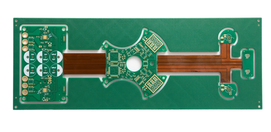
How Are Multilayer Boards Constructed?
The multi-layer board is composed of several single sided PCB for the outer layer and some double-sided PCBs for the inner layer.
l Single-Sided Boards
In the most basic PCB design, components are placed on one side of the board, and the wiring is on the other. This is called a single-sided board. Due to strict routing limitations (since traces cannot cross each other), single-sided boards are mostly used in simpler circuits.
l Double-Sided Boards
Double-sided boards have wiring on both sides. To connect the circuits on both sides, vias (small holes filled or coated with metal) are used. The larger area and ability to route traces through both sides make double-sided boards more suitable for complex circuits compared to single-sided boards.
l Multilayer Boards
To increase routing space, multilayer boards are created by combining multiple layers of single-sided or double-sided boards. For example, a four-layer or six-layer PCB might consist of a double-sided board as the core with single-sided boards on either side, all bonded together. Multilayer boards allow more complex designs, and while most modern PCBs use between 4 to 8 layers, designs with up to 100 layers are possible for advanced computing needs, though they are increasingly rare due to advances in other technologies.
The number of layers doesn’t always indicate the number of wiring layers—some layers may be added purely to adjust board thickness. Most motherboard designs consist of 4 to 8 layers, and while extremely complex multilayer boards were once used in supercomputers, they are now often replaced by clusters of standard machines.
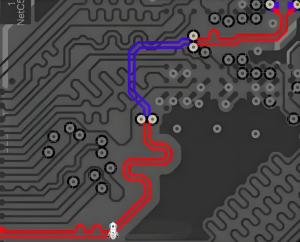
Trace Width and Copper Pour Guidelines
When designing PCBs, a general rule is to use thicker traces for high-current areas (e.g., 50 mil or more) and thinner traces for low-current signals (e.g., 10 mil). In some electromechanical control systems, the instantaneous current through a trace can exceed 100A, in which case thin traces would fail.
An empirical rule of thumb is that 10A can safely pass through 1 square millimeter of trace cross-section. If the trace is too thin, it may burn out under high current. This phenomenon follows the energy equation: Q = I^2*t. For example, a trace designed for 10A can likely handle a sudden current spike of 100A for microseconds, but beyond that, other factors like stray inductance in the trace could generate strong counter-electromotive forces, potentially damaging other components. Longer and thinner traces have higher stray inductance, so their length must also be considered.
Copper Pouring on Vias and Pads
Most PCB design software offers options for how to connect vias or pads to copper planes, such as direct pour, orthogonal spokes, or 45-degree angled spokes. While many designers select based on aesthetics, these choices affect both current capacity and heat dissipation.
l Direct Pour: This method provides the strongest current-carrying capacity for pads or vias, making it ideal for high-power circuits. However, direct pours also enhance heat conduction, which, while beneficial for cooling components, can complicate soldering by rapidly dissipating heat, requiring higher soldering temperatures and larger soldering irons, which may reduce production efficiency.
l Orthogonal and 45-Degree Spokes: These methods reduce the contact area between the pad or via and the copper, slowing heat dissipation and making soldering easier. For low-power signal traces, orthogonal or 45-degree spokes are recommended, while direct pour is necessary for pads carrying high currents. The choice between orthogonal and 45-degree spokes is mainly aesthetic.