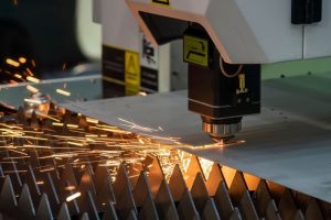
What Is PCB Contract Manufacturing?
PCB contract manufacturing is a process where companies outsource the production of printed circuit boards to a third-party manufacturer. This includes not just making the board, but also assembling components, running functional tests, and sometimes even final product packaging. It allows companies to focus on core tasks like product development and marketing, while the technical side of electronics production is handled by experts.
At its core, PCB contract manufacturing saves time, reduces production costs, and ensures consistency in quality. For startups and global electronics brands alike, finding a dependable contract manufacturer can significantly boost speed-to-market and reduce project risks.

Our Printed Circuit Board Services
At Best Technology, we offer a complete range of services under one roof. Whether you’re developing a new electronic product or scaling up production, we handle everything from the initial design to final functional testing. Here’s what we bring to the table:
- PCB Layout & Design
We help you start from scratch or improve your existing Gerber files. Our layout team is experienced in high-density routing, impedance control, and EMC-compliant designs. With tools like Altium Designer and CAD, we ensure accurate and efficient PCB layouts tailored to your project needs.
- OEM & ODM PCB Manufacturing
Whether you need OEM or ODM service, we have the capability to take your concept and turn it into a working product. Our engineering team collaborates closely with clients to deliver custom solutions that are production-ready.
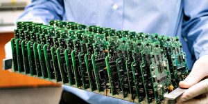
- Electronic Components Assembly
From SMT (Surface Mount Technology) to through-hole assembly, our facility is equipped for full-scale PCBA (Printed Circuit Board Assembly). We support both leaded and RoHS-compliant assembly and offer automated inspection (AOI), X-ray, and BGA rework services to guarantee every joint is solid and reliable.
- Wire Harness Assembly
We also supply PVC/PE/TPU/LZSH hook-up wire, flat cable, connector wire harness for machinery equipment, and cables for the field of electronic appliances, DC power supply, audio video devices, toys, medical equipment, communication devices, electrician & electrical, computer accessories cable, and so on.
- Box Building Assembly
We don’t stop at the board level. If you need enclosure integration, cable harnessing, or full unit assembly, our box building assembly service is available. This end-to-end solution simplifies your supply chain and gives you more control over the finished product.
- Functional Testing
We provide full functional testing based on your test procedure or help you develop one. This includes power-on tests, signal integrity verification, and custom fixture testing. We ensure your board works perfectly before it reaches your customers.

What PCBs We Can Fabricate?
Our team at Best Technology specializes in a wide range of printed circuit board types. No matter your project’s complexity or environment, we’ve got you covered. Here are some products that we can make, but not limited to these PCBs.
- Extra Thin PCB
For devices that require tight packaging like smart cards, cameras, or medical sensors, we offer ultra-thin PCBs as thin as 0.1mm. These boards maintain strength while saving space.
- HDI PCB
High-Density Interconnect (HDI) PCBs support advanced electronics with fine-pitch components, blind and buried vias, and micro-via-in-pad technology. These are perfect for smartphones, tablets, and compact IoT devices.
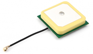
- RF PCB
We manufacture RF (Radio Frequency) PCBs using low-loss materials like Rogers, Taconic, and PTFE laminates. These boards are designed for wireless communication, antennas, and radar systems, where signal clarity matters most.
- Heavy Copper PCB & Busbar PCB
When high current is involved, such as in automotive or industrial power supplies, heavy copper and busbar PCBs are necessary. We can produce boards with copper thickness from 2oz to 20oz, ensuring excellent thermal and electrical performance.
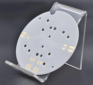
- Metal Core PCB
For LED lighting and power conversion applications, our metal core PCBs (MCPCBs) provide efficient thermal dissipation. Aluminum and copper cores are both available depending on your thermal and mechanical needs.
- Ceramic PCB
Using materials like aluminum nitride and alumina, ceramic PCBs deliver outstanding heat resistance and insulation. We have mature manufacturing technologies, including: Thick film ceramic PCB, thin film ceramic PCB, AMB ceramic PCB, DBC & DPC ceramic PCB, HTCC & LTCC ceramic PCB.
- Flex Circuit & Rigid-Flex PCB
Flex circuits offer excellent bendability, reducing connectors and saving space. Rigid-flex PCBs combine the best of both worlds and are widely used in wearables, drones, and other portable electronics.
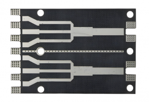
- High-Speed PCB
We design and produce high-speed PCBs with controlled impedance, low-loss materials, and proper stack-ups. These are ideal for applications like 5G networks, servers, and high-frequency digital communication.
- High TG PCB
When operating temperatures exceed 170°C, High-TG (glass transition temperature) PCBs are the right choice. These boards are more stable thermally and mechanically, perfect for automotive and industrial applications.
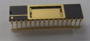
- IC Substrate
We also support packaging solutions with IC substrates that act as a bridge between chips and PCBs. Our substrates offer fine-line traceability and are used in semiconductor packaging.
- Ceramic Packages
Ceramic packages provide superior hermetic sealing and thermal cycling endurance. These are used to package sensitive ICs in defense, aerospace, and critical medical applications.

FR4 PCB Capability in Best Technology
At Best Technology, we offer a wide range of FR4 PCBs — the most common material in the PCB industry — from consumer electronics to industrial control systems and automotive electronics. Whether it’s single-sided, double-sided, or multi-layer (up to 40 layers), we provide:
✅ General Capabilities
- Layer Count: 1–40 layers
- Board Size: Up to 580mm × 1200mm
- Board Thickness: 0.2mm to 3.2mm
- Copper Thickness: 0.5oz to 6oz (outer), 0.5oz to 3oz (inner)
- Finished Hole Size: ≥ 0.10mm
- Minimum Line Width / Spacing: 3mil / 3mil (0.075mm)
- Aspect Ratio: Up to 12:1
- Impedance Control: ±10% or better
✅ Material Options
- Standard FR4: Tg135°C
- High-TG FR4: Tg170°C to Tg180°C
- Halogen-Free FR4: Environmentally friendly for RoHS/REACH applications
- Low Dk/Df FR4: For better signal performance in high-speed circuits
✅ Surface Finishes
- HASL (Hot Air Solder Leveling) – Leaded & Lead-free
- ENIG (Electroless Nickel/Immersion Gold)
- OSP (Organic Solderability Preservatives)
- Immersion Tin / Immersion Silver
- ENEPIG (Electroless Nickel Electroless Palladium Immersion Gold)
- Gold Finger (with beveling & plating options)
✅ Solder Mask & Silkscreen
- Solder Mask Colors: Green, Blue, Red, Yellow, Black, White, Purple, Matte options
- Silkscreen Colors: White, Black, Yellow
- Solder Mask Thickness: 7–40μm
- Min Solder Mask Dam: 0.075mm (3mil)
✅ Drilling & Via Types
- Mechanical Drilling (for standard vias and plated holes)
- Laser Drilling (for microvias and blind/buried vias)
- Via Filling & Capping (VIPPO: via-in-pad plated over)
- Tented, Plugged, and Stacked Vias for HDI applications
✅ Special Capabilities
- Controlled Impedance Tolerance: ±10% (custom up to ±8%)
- Edge Plating / Castellation
- Countersinks & Counterbores
- Peelable solder mask
- Carbon ink printing (for jumpers, contact pads, etc.)
- Via tenting, filling, and plugging with resin
✅ Electrical Testing & Inspection
- 100% E-test (Flying Probe or Bed of Nails)
- AOI (Automated Optical Inspection)
- X-ray for BGA and inner layers
- ICT, FCT, and aging testing available
With a monthly capacity of over 30,000 square meters and a 98% on-time delivery rate, our FR4 line is built to serve both prototypes and mass production.
Certifications & Quality Assurance in PCB Manufacturing
At Best Technology, quality isn’t just a goal — it’s a standard built into every step of our manufacturing process. To ensure compliance with international regulations and industry-specific requirements, we maintain a comprehensive set of certifications, including:
- ISO 9001:2015 – Quality Management System
- ISO 13485:2016 – Medical Device Quality System
- IATF 16949:2016 – Automotive Quality Management
- AS9100D – Aerospace & Defense Quality Management
- UL Certification
- RoHS & REACH Compliance
- IPC Standards Compliance – IPC-A-600 and IPC-A-610 Class 2 & Class 3 for PCBfabrication and assembly
One-Stop High-Quality PCB Contract Manufacturer
When you’re looking for a reliable partner to handle your PCB contract manufacturing, Best Technology is ready to deliver more than just boards. We provide full-service support — from design to delivery — with speed, precision, and attention to detail.
We offer a complete solution that includes PCB fabrication, components sourcing, assembly, testing, and even box build — all under one roof. That means you don’t have to juggle multiple suppliers or waste time coordinating between factories. You get a dedicated project manager, clear communication, and consistent quality from start to finish.
Here’s why companies from over 80 countries trust us with their PCB contract manufacturing needs:
- Engineering Support: this isn’t traditional engineer support, in Best Technology, every sales are engineer, they are professional so that can save much time on design communication and can give you the best solutions.
- Fast Turnaround: we offer quick-turn prototyping (as fast as 24 hours) and competitive lead times for volume production.
- Global Shipping: Whether you’re in the US, Germany, Japan, or Australia, we ship your orders promptly with DHL, FedEx, UPS, air & ocean shipment.
- Traceability System: Our ERP system keeps detailed records for every board we produce, offering transparency and traceability.
- WIP Update Every Week: Every customer can enjoy one-to-one sales-assistant service, they will update the product status & share videos every week for you, so that you can closely to your PCBs.
- Cost-Effective Solutions: With advanced production lines and a mature supply chain, we provide cost-effective options without sacrificing quality.
PCB contract manufacturing can significantly reduce your product development cycle and overhead. By partnering with a professional and certified provider like Best Technology, you ensure every step — from PCB layout to functional testing — meets your project goals with precision and speed.
Whether you need a simple FR4 board or a high-performance ceramic PCB, our comprehensive services and commitment to quality make us a trusted choice for businesses around the world.
Frequently Asked Questions
1. What industries does Best Technology serve?
We serve a broad range of industries including medical, automotive, aerospace, telecom, and consumer electronics.
2. Can Best Technology support low-volume or prototype orders?
Yes, we support both small-batch prototypes and high-volume production with flexible minimum order quantities.
3. Do you offer component sourcing services?
Absolutely. We have partnerships with authorized distributors to source genuine components and manage the BOM for you.
4. What file formats do you accept for PCB layout?
We accept Gerber, ODB++, and other formats such as Altium, Eagle, and CAD-based files.
5. How can I request a quote for PCB contract manufacturing?
Simply send your files and requirements via our online form or email, and our sales team will get back to you within 24 hours.