Burnt solder joint means an overheated, oxidized, or heat-damaged solder connection on a PCB, and it can affect electrical continuity, mechanical strength, and long-term PCBA reliability. This article explains what a burnt solder joint looks like, why it happens, how to judge its risk, how to handle minor cases, and how to prevent it during PCB assembly.
What problems do customers usually face when they find a burnt solder joint?
- The solder joint looks dark or burned, but the real damage level is unclear.
- The PCB may still power on, but long-term reliability is uncertain.
- The root cause is hard to confirm between soldering, design, material, and rework.
- High-current terminals, relays, or connectors may fail again after temporary correction.
- A small soldering defect may delay delivery, increase inspection cost, or affect customer trust.
A reliable PCBA manufacturer should not treat a burnt joint as only a cosmetic issue; it should be reviewed from process, design, and reliability angles.
- We inspect appearance, wetting, pad condition, and copper exposure before judging the risk.
- We use electrical testing, visual inspection, AOI, and engineering review where needed.
- We check soldering temperature, dwell time, flux condition, pad design, and thermal balance.
- We review high-current paths, copper thickness, terminal design, and solder joint geometry.
- We improve process control before mass production to reduce repeat defects and delivery risk.
EBest Circuit (Best Technology) provides PCB manufacturing and PCBA assembly services for industrial electronics, LED products, power modules, automotive electronics, medical devices, and other reliability-focused applications. With experience in PCB fabrication, SMT assembly, DIP assembly, functional testing, and engineering review, we help customers reduce soldering defects before they become field failures. For PCB or PCBA projects, you can contact us at sales@bestpcbs.com.
What Is a Burnt Solder Joint?
A burnt solder joint is a soldered connection that has been exposed to excessive heat, repeated heating, poor soldering conditions, or severe oxidation during assembly or rework. In simple terms, it is not just “dark solder.” It may indicate that the solder, pad, flux residue, component lead, or PCB surface has been overheated.
In PCB assembly, a solder joint has two basic jobs. It must provide a stable electrical path and also hold the component lead or terminal mechanically. When heat is not controlled well, the solder joint may lose its smooth metallic surface, the flux may carbonize, and the copper pad may become weak or contaminated.
A burnt solder joint may appear in several situations:
| Situation | Typical Condition |
|---|---|
| Manual Soldering | Excessive heat |
| Rework | Repeated heating |
| High-Current Area | Local overheating |
| Poor Wetting | Oxide or low flux |
| PCB Damage | Lifted pad or trace damage |
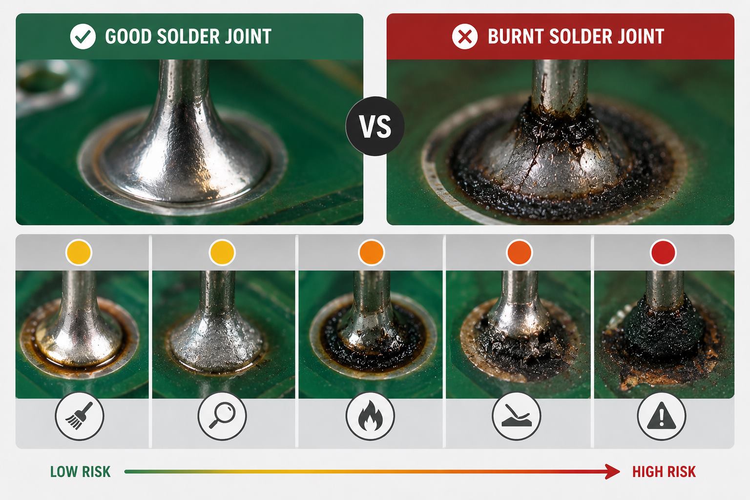
A light brown mark around a solder joint may only be flux residue. A blackened pad, lifted copper, cracked solder, or burned laminate is more serious. That is why the joint should be judged by both appearance and function.
In short, a burnt solder joint is a warning sign. It may be minor residue, but it may also point to overheating, weak bonding, or future reliability failure.
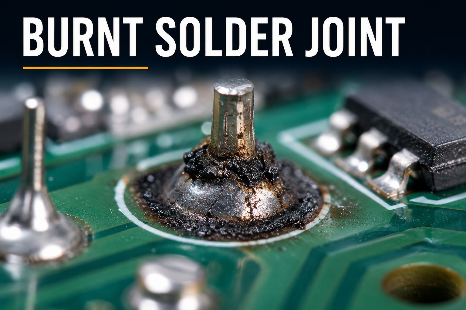
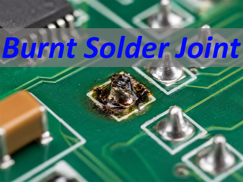
What Does a Burnt Solder Joint Look Like?
A burnt solder joint usually looks darker, rougher, or more contaminated than a normal solder joint. A good solder joint often has a smooth, bright, and well-wetted appearance, although lead-free solder may look slightly dull compared with leaded solder. A burnt joint, however, tends to show heat stress, oxidation, or carbonized residue.
The most common visual signs include:
- Dark brown or black residue around the solder joint.
- Dull, grainy, or rough solder surface instead of a clean fillet.
- Blackened component lead or terminal near the solder area.
- Discolored solder mask around the pad.
- Lifted or loose copper pad after repeated heating.
- Cracked or uneven solder fillet caused by poor wetting or heat stress.
- Burned PCB laminate in severe cases.
For users searching what a burnt solder joint looks like, the key is to separate harmless residue from actual joint damage. Flux residue can look brown after soldering, especially when the board is not cleaned. But if the solder does not wet the pad, the pad turns black, or the board material is visibly scorched, the risk is much higher.
A practical visual comparison is shown below:
| Appearance | Possible Meaning | Risk Level |
|---|---|---|
| Slight brown residue | Flux residue | Low |
| Dull solder surface | Oxidation or poor wetting | Medium |
| Black pad edge | Overheating or contamination | Medium to high |
| Lifted pad | PCB copper damage | High |
| Burned laminate | Severe heat damage | High |
Visual inspection is the first step, not the final answer. A burnt-looking solder joint should still be checked for wetting quality, pad strength, electrical continuity, and the surrounding PCB condition.
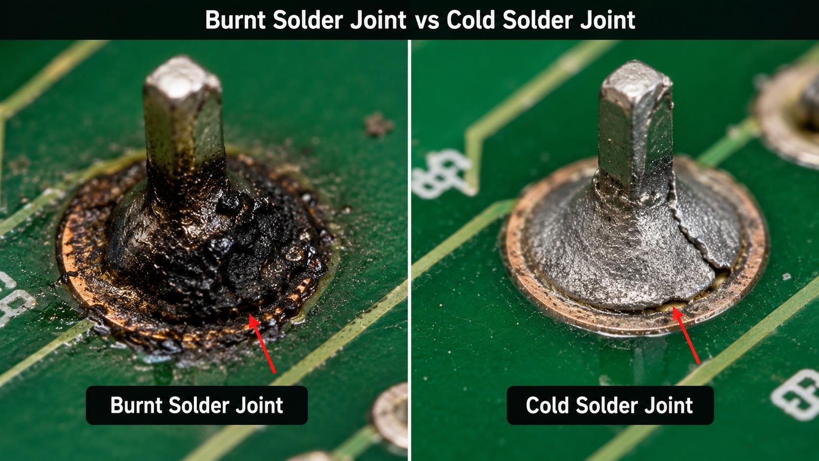
Burnt Solder Joint vs Cold Solder Joint: What Is the Difference?
A burnt solder joint and a cold solder joint may both look dull, weak, or unreliable, but they are caused by different soldering problems. A burnt joint is usually related to too much heat or repeated heating. A cold solder joint is usually caused by insufficient heat, movement during cooling, or poor wetting.
This difference matters because the prevention method is not the same. If the issue is cold soldering, the process may need better heat transfer, cleaner pads, or correct reflow temperature. If the issue is burnt soldering, the process may need lower heat, shorter dwell time, better tip selection, or improved rework control.
| Item | Burnt Solder Joint | Cold Solder Joint |
|---|---|---|
| Main cause | Excessive heat | Insufficient heat |
| Common appearance | Dark, scorched, oxidized | Dull, rough, cracked |
| Flux condition | May be carbonized | May be poorly activated |
| Pad condition | May be discolored or lifted | Usually not burned |
| Main risk | Heat damage and weak bonding | Poor electrical and mechanical connection |
| Prevention focus | Heat control | Proper wetting and stable heating |
A cold solder joint often forms when solder does not fully flow and bond to the pad or lead. A burnt solder joint often happens when heat is applied too aggressively or for too long. In some cases, a joint can show both problems: the operator keeps heating a dirty or oxidized pad, but solder still does not wet properly, so the area becomes burned.
The best way to judge the difference is to inspect the solder fillet, pad surface, component lead, and surrounding laminate together. The surface alone can be misleading.
What Causes a Burnt Solder Joint During Soldering?
A burnt solder joint usually comes from a mismatch between heat, time, surface condition, and solderability. The problem is rarely caused by one factor only. In real PCB assembly, it often comes from a combination of excessive temperature, poor wetting, wrong tools, and repeated rework.
Common causes include:
- Soldering iron temperature is too high.
When the iron is much hotter than required, flux burns quickly and the solder surface oxidizes faster. - Contact time is too long.
Even a reasonable temperature can damage the pad if the iron stays on the joint too long. - The soldering tip is not suitable.
A tip that is too small may force the operator to heat longer. A dirty tip may transfer heat poorly. - Flux is insufficient or burned out.
Flux removes oxides and helps solder flow. Without active flux, the operator may keep heating the joint without achieving proper wetting. - Pad or component lead is oxidized.
Oxidation blocks solder bonding. More heat does not always solve this problem; it can make it worse. - The PCB has large copper areas near the pad.
Ground planes, power planes, and heavy copper areas absorb heat, making soldering more difficult. - Repeated rework overheats the same pad.
Each heating cycle increases the risk of lifted pads, damaged solder mask, and delamination.
The soldering process must balance temperature and time. More heat is not always better. A stable process uses suitable flux, correct tip size, proper preheating where needed, and controlled dwell time.
The root cause of a burnt solder joint is usually poor thermal control. To prevent it, the process should be reviewed before blaming only the operator.
What Problems Can a Burnt Solder Joint Cause on a PCB?
A burnt solder joint can create cosmetic, electrical, mechanical, and reliability problems. Some boards may pass a simple power-on test, but still fail later under vibration, thermal cycling, or high current load. That is why burnt joints should not be ignored in professional PCBA production.
The main risks include:
- Unstable electrical connection
Oxidized or poorly wetted solder may increase contact resistance. - Intermittent failure
The board may work during testing but fail after movement, vibration, or temperature change. - Weak mechanical strength
A poor solder fillet may not hold a connector, terminal, relay, or through-hole component firmly. - Local heat buildup
High resistance at the joint can generate heat, especially in current-carrying circuits. - Pad lifting or trace damage
Excessive heat can weaken the bond between copper and laminate. - Carbonized residue contamination
Burned flux or PCB material may affect cleanliness, insulation, or inspection clarity. - Lower customer confidence
Even when the function is normal, visible burn marks can raise serious quality concerns.
For low-power signal circuits, a slightly overheated joint may still pass inspection after cleaning and testing. For power electronics, relays, terminals, motor control boards, LED drivers, and automotive PCBA, the risk is higher because current, heat, and vibration are more demanding.
A burnt solder joint is not always a failure, but it is always a signal that the joint deserves closer review.
How to Check Whether a Burnt Solder Joint Is Still Reliable?
Checking a burnt solder joint requires more than looking at color. A reliable judgment should combine visual inspection, mechanical condition, electrical performance, and process history. The goal is to decide whether the joint is acceptable, needs correction, or indicates a deeper PCB assembly issue.
A practical inspection flow includes:
- Visual inspection
Check solder shape, wetting angle, pad color, residue, cracks, and solder mask damage. - Magnification review
Use a microscope or inspection camera to check fine cracks, lifted pads, and incomplete wetting. - Continuity testing
Confirm that the electrical path is connected. - Resistance check
For power paths, compare resistance with expected values or a known good board. - Mechanical check
Gently verify whether the component lead, connector, or terminal is stable. - Thermal review
For high-current joints, check whether the area heats abnormally during operation. - Process review
Confirm whether the joint was manually reworked, repeatedly heated, or exposed to abnormal soldering conditions.
A simple pass/fail approach is not always enough. For example, a burnt joint may pass continuity testing but still have weak mechanical bonding. A connector joint may look acceptable but fail after repeated plugging and unplugging. A relay joint may work at low load but heat up under real current.
The safest judgment comes from combining inspection data with application requirements. If the PCBA is used in medical equipment, automotive electronics, industrial control, or high-power LED systems, the acceptance standard should be stricter.
How to Fix a Burnt Solder Joint Without Damaging the PCB?
This section should be understood as basic handling guidance, not as the main focus of the article. For a professional PCB or PCBA supplier, the more important goal is to prevent burnt solder joints in production. Still, when a minor burnt solder joint appears, proper handling can reduce the risk of further PCB damage.
A controlled method may include:
- Stop adding heat immediately
Do not keep heating a joint that is not wetting properly. - Clean the area first
Remove carbonized flux residue with a suitable cleaning agent. - Inspect the pad and trace
Check whether the pad is lifted, cracked, or detached from the PCB. - Apply fresh flux
Fresh flux helps solder flow and reduces unnecessary heating time. - Remove oxidized solder if needed
Use solder wick or a desoldering tool carefully. - Reflow with controlled heat
Use the correct tip size, stable temperature, and short contact time. - Inspect again after cooling
Confirm solder wetting, pad condition, and electrical continuity.
For SEO coverage, users may search how to fix a burnt solder joint or burnt solder joint repair, but in manufacturing practice, repair should never replace root-cause control. If the pad is lifted, the laminate is burned, or the trace is damaged, the board should be reviewed by an experienced PCBA engineer before use.
Minor cases may be corrected. Severe cases should be treated as a reliability risk, not just a soldering mark.
Why Do High-Current Components Have a Higher Risk of Burnt Solder Joints?
High-current components have a higher risk because their solder joints must carry more current, handle more heat, and often connect to larger copper areas. Relays, power terminals, connectors, MOSFETs, transformers, inductors, and LED power input pads all place extra stress on solder joints.
The risk comes from both production and operation:
| High-Current Factor | Why It Matters |
|---|---|
| Large copper area | Absorbs heat during soldering |
| Thick leads or terminals | Need more heat to solder properly |
| Higher current | Increases heat at weak joints |
| Mechanical stress | Connectors and terminals may move |
| Rework difficulty | More heating may damage pads |
| Poor solder volume | Reduces current-carrying stability |
A common real-world example is a heater relay solder joint on an appliance control board. Some users even search specific phrases such as Bosch dishwasher control board burnt heater relay solder joint. The actual lesson is broader: relay joints and heater circuits often carry higher current, so a weak solder joint may heat up, discolor, crack, or burn over time.
For high-current PCBA design, soldering quality is only one part of the answer. The design should also consider:
- Copper thickness
- Pad size
- Thermal relief design
- Connector current rating
- Solder volume
- Trace width
- Heat dissipation path
High-current solder joints need both good process control and proper PCB design. If either side is weak, the joint may become a heat concentration point.
How to Prevent Burnt Solder Joints in PCB Assembly?
Preventing burnt solder joints requires process control, design review, material control, and inspection. The goal is not simply to tell operators to “use less heat.” A stable PCBA process should make correct soldering easier and repeatable.
Key prevention methods include:
- Set suitable soldering temperature
Manual soldering temperature should match solder type, component size, copper area, and process requirement. - Control heating time
Short, effective heating is safer than long contact time with poor heat transfer. - Use the right soldering tip
A suitable tip improves heat transfer and reduces unnecessary dwell time. - Apply proper flux
Flux improves wetting and reduces oxidation during soldering. - Keep pads and leads clean
Oxidized surfaces need cleaning or replacement, not excessive heating. - Review thermal relief design
Pads connected to large copper planes may need balanced thermal relief to improve solderability. - Use preheating when appropriate
Thick copper boards, large ground planes, and high-mass components may need controlled preheating. - Avoid repeated uncontrolled rework
Rework should follow a defined process to protect pads and laminate. - Strengthen inspection
AOI, visual inspection, first article inspection, and functional testing help catch problems early. - Review DFM before production
A design-for-manufacturing review can identify soldering risks before assembly starts.
For professional PCBA production, prevention is always more valuable than correction. A burnt solder joint often appears at the soldering stage, but its cause may begin in pad design, copper layout, component selection, or process planning.
The best prevention strategy is to combine engineering review with stable production control.
FAQs about Burnt Solder Joint
Q1: Is a burnt solder joint always bad?
A1: Not always. A slight brown mark may be flux residue, but a blackened pad, cracked solder, lifted pad, or burned laminate should be treated as a reliability risk.
Q2: Can a burnt solder joint still conduct electricity?
A2: Yes, it may still conduct electricity during a simple test. However, conduction alone does not prove long-term reliability, especially under heat, vibration, or high current.
Q3: What does a burnt solder joint look like?
A3: It may look dark, rough, dull, blackened, or surrounded by brown residue. In severe cases, the PCB pad or laminate may also be discolored.
Q4: What causes a burnt solder joint?
A4: Common causes include excessive soldering temperature, long heating time, dirty pads, poor flux activity, oxidized leads, large copper areas, and repeated rework.
Q5: What is the difference between a burnt solder joint and a cold solder joint?
A5: A burnt solder joint is usually caused by too much heat. A cold solder joint is usually caused by insufficient heat, poor wetting, or movement before the solder fully solidifies.
Q6: Can I fix a burnt solder joint by adding more solder?
A6: Adding more solder alone is not a good solution. The area should be cleaned, inspected, fluxed, and reflowed correctly. If the pad is damaged, engineering review is needed.
Q7: Why do relay solder joints burn more often?
A7: Relay joints often carry higher current and may experience heat buildup if solder wetting, pad design, or copper thickness is not suitable.
Q8: How can a PCBA manufacturer prevent burnt solder joints?
A8: A PCBA manufacturer can prevent them through proper temperature control, flux use, pad design review, thermal relief optimization, operator training, inspection, and DFM review.
Q9: Are burnt solder joints common in hand soldering?
A9: They can happen in hand soldering when the iron is too hot, the tip is dirty, the operator heats the pad too long, or the surface does not wet properly.
Q10: Should burnt solder joints be accepted in mass production?
A10: They should be reviewed carefully. Minor residue may be acceptable after cleaning and inspection, but visible heat damage, weak wetting, or pad damage should not be ignored.
All in all, burnt solder joint means an overheated or heat-damaged solder connection, and it plays an important role in judging PCB assembly quality and long-term PCBA reliability. This article explained what it looks like, why it happens, how it differs from a cold solder joint, how to check the risk, and how to prevent it during PCB assembly.
For buyers and engineers, the most important point is not only how to fix a visible joint, but how to stop the same problem from entering production again. Burnt solder joints are often connected with heat control, pad design, copper area, component type, and inspection standards.
EBest Circuit (Best Technology) supports customers with PCB fabrication, PCBA assembly, DFM review, soldering process control, functional testing, and quality inspection. If your project involves industrial control PCB, power PCBA, LED PCB, automotive electronics, control boards, connectors, relays, or high-current circuits, our engineering team can help review the manufacturing risks before production.
For PCB and PCBA project support, please contact sales@bestpcbs.com.