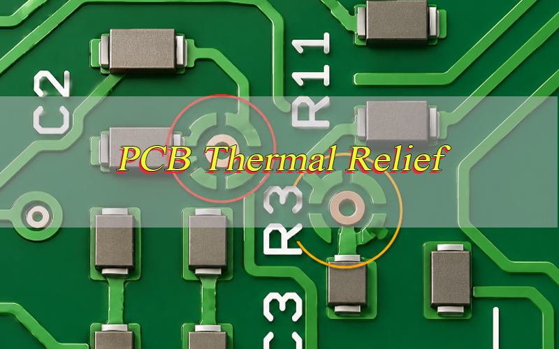
PCB thermal relief is useful for soldering, but in high-current circuits it must be designed carefully. A thermal relief structure uses copper spokes to connect a pad, via, or plated hole to a copper plane. This improves solderability, yet it also reduces the copper cross-section available for current flow.
In low-current areas, this trade-off is usually acceptable. In power input terminals, motor control circuits, LED power boards, automotive PCB assemblies, and heavy copper PCB designs, the same structure may create heat rise, voltage drop, or weak current paths. High-current PCB thermal relief design should balance soldering quality with electrical and thermal reliability.
What Is PCB Thermal Relief in High-Current Circuit Design?
PCB thermal relief in high-current circuit design is a controlled copper connection between a power pad, via, or plated hole and a large copper area. Instead of using a full solid connection, the pad connects to the plane through several copper spokes.
These spokes are also called thermal spokes, spoke connections, or relief connections. They reduce heat loss during soldering, helping the pad reach soldering temperature more easily. This is useful when a large copper plane would otherwise pull heat away too fast.
However, high-current circuits are different from ordinary signal circuits. The copper spokes must carry real load current. If the spokes are too narrow, too few, or too long, they may become a current bottleneck, causing heat rise, higher resistance, or reduced long-term reliability.
How Does PCB Thermal Relief Affect Current Flow and Heat Transfer?
PCB thermal relief affects current flow by reducing the effective copper area between the pad and the copper plane. Current must pass through the spokes instead of spreading through a full copper connection.
At the same time, the structure also limits heat transfer. This is helpful during soldering because the pad does not lose heat too quickly. But after the product starts working, the same limited copper path may reduce heat dissipation from power pins, terminals, and hot components.
This is the main design conflict. A narrow thermal relief connection improves solderability, but it may increase current density. A solid copper connection improves current flow and heat spreading, but it may make soldering harder. For high-current PCB, the connection style should be selected by current level, copper thickness, pad size, operating temperature, and soldering process.
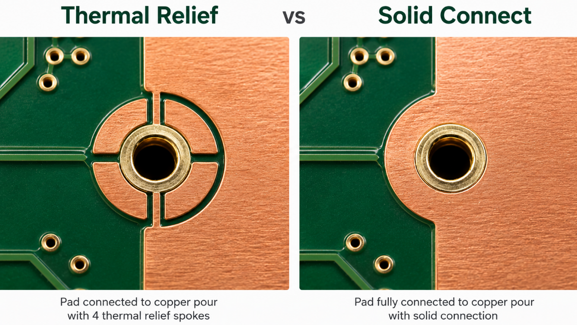
Thermal Relief vs Solid Connect: Which Is Better for High-Current PCB?
For high-current PCB, solid connect is usually safer when current capacity and heat dissipation are the priority. Thermal relief is only suitable when solderability is difficult and the spokes are wide enough to carry the required current.
| Item | Thermal Relief | Solid Connect | Better Choice |
|---|---|---|---|
| Current capacity | Limited by spoke width, spoke count, and copper thickness | Higher because the pad connects fully to copper | Solid connect |
| Heat dissipation | Lower, because spokes restrict heat flow | Better heat spreading into copper plane | Solid connect |
| Solderability | Easier to solder, especially on large copper planes | Harder to solder due to fast heat loss | Thermal relief |
| Voltage drop | Higher risk if spokes are narrow | Lower resistance path | Solid connect |
| Temperature rise | May increase around spokes under load | Lower local heating in most power paths | Solid connect |
| Mechanical strength | Weaker if spokes are thin or long | Stronger copper support around pad | Solid connect |
| Through-hole power pins | Useful if solder fill is difficult, but spokes must be enlarged | Better for sustained current | Case by case |
| Power terminals | Risky with default narrow spokes | More reliable for high load and cable stress | Solid connect |
| Connectors | Suitable for low-current or ground pins | Better for high-current power pins | Mixed rules |
| Thermal vias | Usually not recommended | Better for heat transfer | Solid connect |
| Heavy copper PCB | Requires wider custom spokes | Often preferred for current paths | Solid connect |
| Rework | Easier pad heating | More difficult due to copper heat sinking | Thermal relief |
| Best use | Moderate current with soldering risk | High current, heat spreading, low resistance | Depends on priority |
A practical choice is simple: use solid connect for sustained high current, thermal pads, bus bars, and heat-spreading areas. Use thermal relief only when soldering risk is higher than current risk. For connectors, mixed rules are often best: signal or ground pins may use relief, while power pins use solid copper or enlarged spokes.
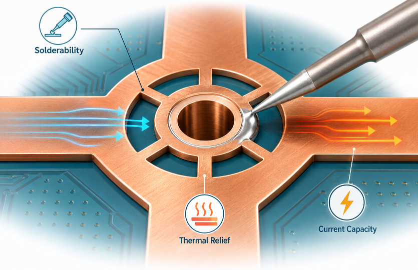
PCB Thermal Relief Spokes: Width, Number, and Copper Thickness Rules
PCB thermal relief spokes are the most important factor in high-current relief design. Spoke width, spoke count, copper thickness, and spoke length all affect current capacity and heat rise.
Key design rules include:
- Use wider spokes for high-current nets.
Narrow spokes create higher resistance and higher current density. Power nets, battery terminals, motor outputs, and high-load connectors should not use small default spokes. - Increase spoke count when space allows.
Four spokes usually provide better current distribution than two spokes. For high-current pads, more copper paths can reduce the load on each spoke. - Match spoke width with copper thickness.
A spoke setting that works on 1 oz copper may not be enough for a high-current heavy copper PCB. Thicker copper can carry more current, but the spoke geometry still needs enough width. - Avoid long and thin spokes.
Longer spokes increase resistance and reduce heat transfer. A large thermal relief gap may improve solderability, but it can weaken current performance. - Use symmetrical spoke placement.
Symmetrical spokes help current distribute more evenly and support more consistent solder wetting.
For many standard boards, 0.20–0.50 mm may be a common starting range, but high-current PCB often requires wider custom spokes. Final values should be checked against current load, copper weight, and temperature rise.
PCB Thermal Relief Gap: How Much Clearance Is Proper for High-Current Pads?
PCB thermal relief gap should be large enough to support soldering, but not so large that it creates long, weak spokes. The gap is the clearance between the pad and the surrounding copper pour.
A typical starting range may be around 0.20–0.50 mm, depending on pad size, copper thickness, voltage clearance, and fabrication capability. For high-current pads, the gap should be reviewed carefully because it directly affects spoke length.
If the gap is too small, soldering may still be difficult because the copper plane pulls away heat quickly. If the gap is too large, the spokes become longer, resistance increases, and current capacity may drop. A proper gap should support solder wetting while keeping enough copper for stable current flow.
For power pads, terminal blocks, and heavy copper areas, the gap should not be selected only for assembly convenience. It should be checked together with spoke width and copper thickness.
PCB Thermal Relief Pad Design for Power Terminals and Connectors
PCB thermal relief pad design for power terminals and connectors should follow the actual pin function, not the footprint shape alone. Power terminals usually carry more current, face stronger mechanical stress, and connect to larger copper areas than ordinary signal pads.
Key design points include:
- Separate power pins from signal pins.
Power pins, ground pins, shield pins, and signal pins should not use one shared copper connection rule. High-current power pins usually need solid connect, wider spokes, or more spokes, while low-current signal pins may use standard thermal relief. - Check real current before setting spokes.
A connector rated for high current does not mean every pin carries the same load. Review continuous current, peak current, and current-sharing between pins. If one pin carries most of the load, narrow spokes may create local heating. - Use solid connect for sustained high-current terminals.
Battery inputs, screw terminals, DC input pads, relay outputs, motor outputs, and bus bar pads often work better with solid copper. These pads need low resistance, better heat spreading, and stronger copper support. - Use enlarged thermal relief only when soldering is difficult.
If a through-hole terminal connects to a large copper plane and solder fill is poor, thermal relief can help. In this case, use wider spokes, four-spoke layout, or customized copper connection instead of default narrow spokes. - Protect pads under mechanical load.
Connectors may experience cable pulling, insertion force, vibration, or repeated mating cycles. Thin spokes can weaken pad support. For mechanically stressed pads, stronger copper connection and larger annular ring are safer. - Review solder fill for through-hole terminals.
Large copper areas can pull heat away and cause insufficient barrel fill. Thermal relief can improve soldering, but it must still support the required current. A DFM and assembly review should check both solderability and load capacity. - Use mixed rules for complex connectors.
One connector may need different rules in the same footprint. Signal pins can use standard relief, ground pins can use wider relief, and power pins can use solid copper. This gives better control than one global setting.
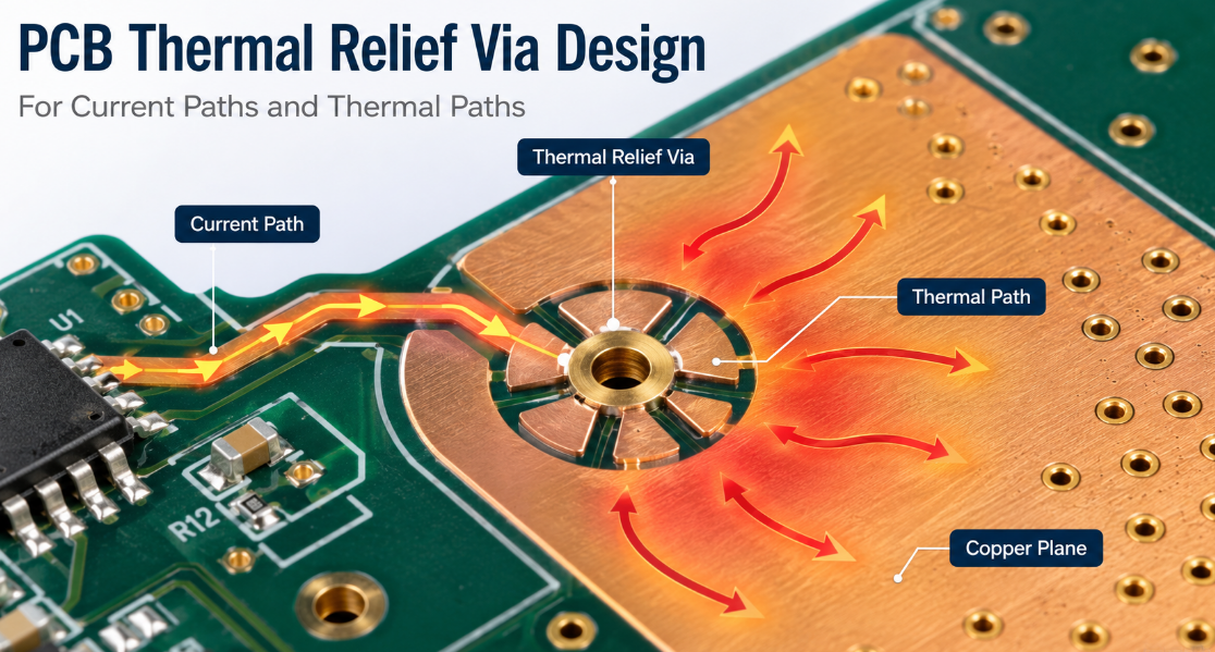
PCB Thermal Relief Via Design for Current Paths and Thermal Paths
PCB thermal relief via design should separate current vias, solderable vias, and thermal vias. These via types serve different functions, so they should not share one default rule.
For high-current vias, solid connection is often preferred. Current vias should provide low resistance between layers, especially in power distribution, battery circuits, motor drives, and heavy copper PCB designs. If thermal relief is added to these vias, the spokes may limit current flow.
For thermal vias under power ICs, MOSFETs, LEDs, and heat-generating components, solid connection is usually better. These vias are used to transfer heat into inner copper planes or bottom copper areas. Thermal relief would reduce the heat path and weaken cooling performance.
Thermal relief can be useful when a via is also a solderable test point, jumper point, or hand-rework feature. In that case, solderability may matter more than maximum current or heat transfer. The via rule should always follow the via function.
When Should High-Current PCB Avoid Thermal Relief?
High-current PCB should avoid thermal relief when the connection must carry sustained current, spread heat, or keep impedance low. In these areas, solid copper usually gives safer electrical and thermal performance.
Avoid or limit thermal relief in these areas:
- Power input terminals with sustained load current.
- Battery connector pads where voltage drop is critical.
- Motor driver outputs with high current pulses.
- MOSFET drain pads used for heat spreading.
- Power IC exposed pads that transfer heat to copper planes.
- LED thermal pads on aluminum PCB or copper core PCB.
- Copper bus bar connections and heavy copper paths.
- RF ground pads where low impedance is important.
- Thermal via arrays under hot components.
Thermal relief may still be used when soldering risk is higher than current risk, but the setting should be customized. Default narrow spokes are rarely suitable for demanding power circuits.
How to Balance Solderability and Current Capacity in High-Current PCB Thermal Relief?
High-current PCB thermal relief design should balance soldering quality, current capacity, voltage drop, and temperature rise. The goal is not to use thermal relief everywhere. The goal is to choose the copper connection that fits the working condition.
Use this decision logic:
- Start from the current path.
Identify where current enters, exits, and spreads through the copper plane. If the relief spokes become the narrowest part of the path, they may control the real current capacity. - Use solid connect when current is the main risk.
If the pad carries sustained high current, pulse current, or heat from a power device, solid copper usually gives lower resistance and lower temperature rise. - Use thermal relief when soldering is the main risk.
If the pad connects to a large plane and soldering is difficult, thermal relief may be useful. The spokes should be enlarged enough to avoid current bottlenecks. - Use wider or multi-spoke relief when both risks exist.
For moderate-to-high current pads that are also hard to solder, use wider spokes, four spokes, or customized copper windows. This improves soldering while keeping more copper area. - Check voltage drop across the connection.
Even a short spoke can add resistance if it is too narrow. In low-voltage power circuits, small voltage loss may affect efficiency, output stability, or thermal behavior. - Check temperature rise under real load.
A layout may pass visual inspection but still create hot spots. For high-current boards, temperature rise should be checked by calculation, first article testing, or thermal measurement. - Match the choice with assembly method.
Hand soldering, wave soldering, selective soldering, and reflow soldering do not behave the same. A pad that is easy to solder in reflow may still be difficult during manual repair. - Avoid using default CAD rules for power nets.
Default relief settings are often created for general solderability, not sustained current. High-current nets should use separate design rules.
A good design keeps the joint solderable without turning the spokes into weak current paths. If current, heat, or mechanical stress is high, stronger copper should take priority.
Is There a PCB Thermal Relief Calculator for High-Current Design?
A PCB thermal relief calculator can be used as a reference for spoke current capacity, resistance, voltage drop, and temperature rise, but it cannot replace layout review or real-load testing. Thermal relief is not a simple straight trace because current spreads through pads, spokes, planes, solder, and nearby copper.
A useful calculation should include spoke width, spoke count, copper thickness, spoke length, current load, allowed temperature rise, copper weight, board material, airflow, and nearby copper area. The total copper cross-section of all spokes is more important than one single spoke width.
A practical workflow is simple. First, define the continuous current and peak current. Then check the copper thickness and available pad space. Next, estimate whether the total spoke width can carry the load with acceptable voltage drop. After that, review whether the same spoke setting still allows good solder wetting.
The calculator result should be treated as an early design check. For power terminals, motor control PCB, automotive PCB, LED PCB, heavy copper PCB, and copper bus connections, the final decision should include DFM review, first article inspection, soldering feedback, and thermal rise testing.
Common PCB Thermal Relief Mistakes in High-Current Circuits
The most common mistake is using default thermal relief settings on high-current pads. High-current PCB needs controlled copper connection rules because small layout details can affect current flow, heat rise, soldering, and reliability.
| Mistake | Risk | Solution |
|---|---|---|
| Narrow spokes on power pads | Hot spots, voltage drop | Increase spoke width or use solid connect |
| Only two spokes on high-current pads | Uneven current distribution | Use four spokes or custom copper connection |
| Thermal relief on thermal vias | Poor heat transfer | Use solid via-to-plane connection |
| Same rule for all connector pins | Weak power path | Separate rules by pin function |
| Oversized relief gap | Long and weak spokes | Reduce gap or widen spokes |
| Ignoring copper thickness | Wrong current estimate | Match relief settings with copper weight |
| Relief on MOSFET or LED thermal pads | Higher device temperature | Use solid copper and thermal vias |
| No load testing | Hidden temperature rise | Test first article under working current |
| Only focusing on solderability | Long-term reliability risk | Check current, heat, and soldering together |
A practical fix starts at the rule level. Create separate copper connection rules for signal nets, ground nets, power nets, thermal vias, connectors, and heavy copper areas. Then review high-current pads manually instead of relying only on automatic copper pour settings.
During production review, check Gerber data, copper thickness, spoke geometry, pad size, annular ring, soldering method, and expected load current. For critical boards, use thermal rise testing or current loading tests before mass production. This helps find hot spots before the product reaches the field.
FAQs About PCB Thermal Relief in High-Current PCB Design
Q1. Can a power connector use different copper rules on different pins?
A1. Yes. A power connector can use mixed copper rules by pin function. Signal pins may use normal relief, ground pins may use wider relief, and high-current power pins may use solid connect. This is often better than applying one setting to the whole connector footprint.
Q2. Why do high-current pads become hot even when the trace is wide enough?
A2. The pad connection may be the bottleneck. A wide trace does not help if current must pass through narrow thermal spokes before reaching the plane. Check spoke width, spoke count, gap, copper thickness, and the full current path from pad to copper area.
Q3. Is four-spoke thermal relief always suitable for power pads?
A3. No. Four spokes are better than two in many cases, but they may still be too narrow for high current. The total spoke width, copper thickness, current load, and temperature rise decide whether the design is safe. Some power pads still require solid copper.
Q4. Can solder added to the pad increase current capacity?
A4. Solder can add some conductive material, but it should not be used as the main current path. Copper carries current much better than solder. The PCB copper design should already support the required current before relying on solder thickness or solder fill.
Q5. Should battery pads use thermal relief?
A5. Battery pads usually need strong copper connection because voltage drop and heat rise are important. Thermal relief may help soldering, but default narrow spokes can reduce reliability. For battery input pads, solid connect or enlarged custom relief is often a safer choice.
Q6. How can I tell if a thermal relief setting is too weak?
A6. Warning signs include narrow spokes, long spokes, high load current, visible copper bottlenecks, or hot spots during testing. If the thermal image shows heat concentrated at the pad connection, the relief pattern may be too weak and should be widened or changed to solid connect.
Q7. Is thermal relief acceptable for screw terminal pads?
A7. It depends on current and soldering difficulty. Screw terminals often carry high current and face mechanical stress, so solid connect is common. If solder fill is difficult, use wider spokes or selective relief, but avoid thin spokes that weaken current capacity and pad strength.
Q8. Does heavy copper always solve thermal relief problems?
A8. No. Heavy copper helps current capacity, but the spoke geometry still matters. If the relief spokes are too narrow, they can still limit current. Heavy copper also pulls heat faster during soldering, so spoke width, gap, and assembly method must be reviewed together.
Q9. Can thermal relief be used in automotive high-current PCB?
A9. Yes, but it should be reviewed carefully. Automotive PCB may face vibration, temperature cycling, and sustained current. Thermal relief may be acceptable for soldering-sensitive pins, but power pads, relay outputs, motor lines, and thermal paths often need solid copper or enlarged connections.
Q10. What should be checked before sending high-current PCB files to production?
A10. Check current paths, copper thickness, spoke width, spoke count, gap, pad size, connector pin function, via connection, soldering process, and expected temperature rise. For power boards, also provide load current, working temperature, and heat-generating component details to the PCB manufacturer.
Q11. Why is thermal relief risky under MOSFET drain pads?
A11. MOSFET drain pads often use copper as both an electrical and thermal path. Thermal relief can restrict heat spreading and increase local temperature. For power MOSFET areas, solid copper, wide copper pours, and thermal via arrays are usually better for heat transfer.
Q12. What information helps a manufacturer review high-current thermal relief?
A12. Gerber files, stackup, copper thickness, BOM, current requirement, load condition, assembly method, and thermal notes are useful. These details help the manufacturer review whether power pads, connector pins, vias, and copper pours can support both soldering and long-term operation.
Conclusion
PCB thermal relief in high-current circuits should be selected by current capacity, heat transfer, solderability, and long-term reliability. Thermal relief can make power pads easier to solder, but narrow spokes may create voltage drop and heat rise under real load. For power terminals, high-current connectors, thermal vias, MOSFET pads, LED heat pads, and heavy copper paths, solid connect or enlarged spoke design is often safer.
The best design depends on copper thickness, spoke width, spoke count, gap, pad function, and assembly method. EBest Circuit is a China-based source PCB and PCBA manufacturer supporting custom fabrication, layout review, DFM checking, and global delivery. For high-current PCB thermal relief design review, prototype orders, or bulk PCB manufacturing, send your files and requirements to sales@bestpcbs.com.