





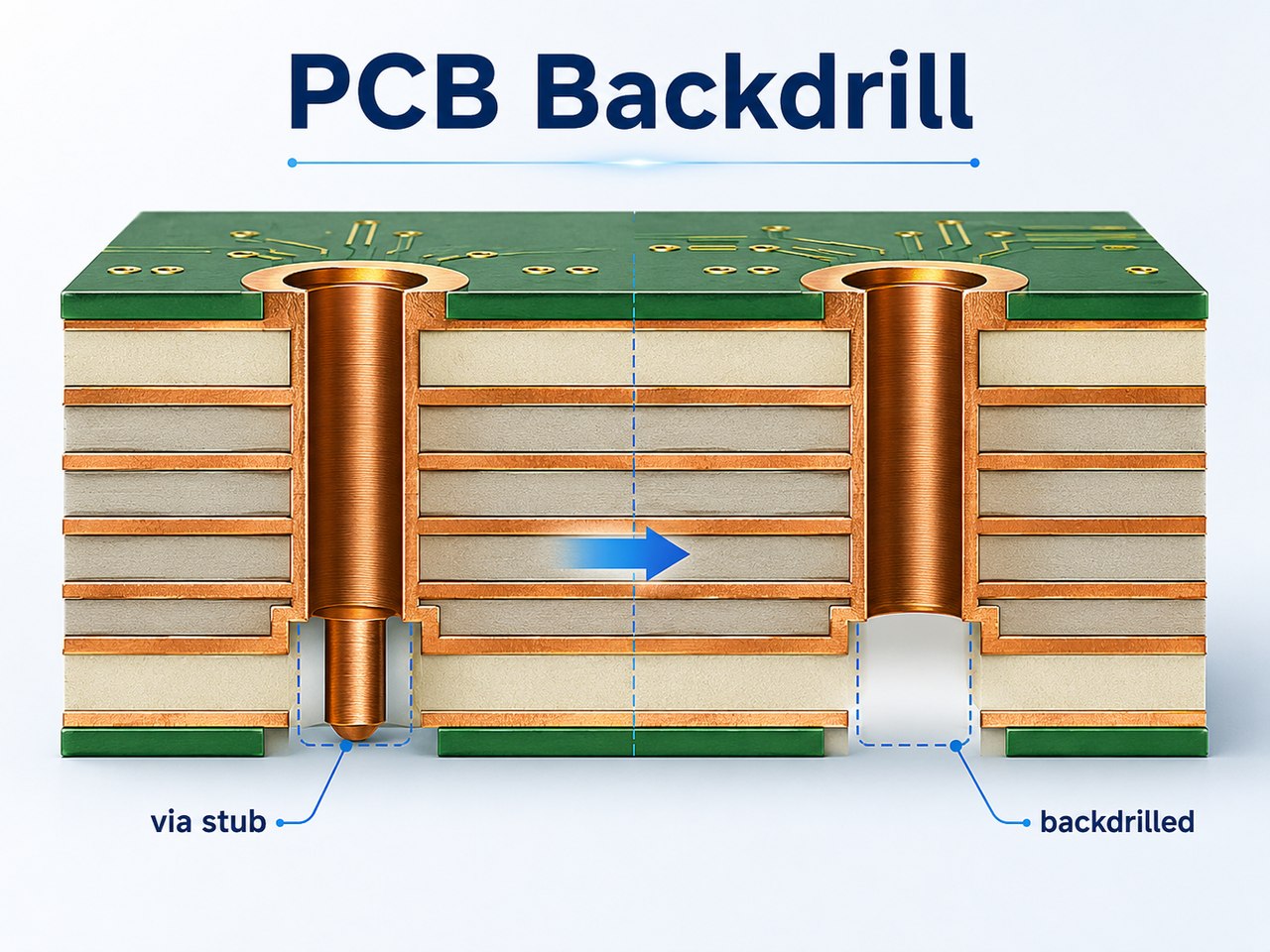
PCB backdrill is a controlled-depth drilling process that removes the unused copper barrel of a plated through-hole. It is mainly used on thick, high-layer-count PCBs carrying fast digital signals.
The process can improve channel performance, but it also adds drill programs, inspection work, and fabrication cost. The decision should be based on actual via geometry and signal-integrity results rather than data rate alone.
What Is PCB Backdrill?
PCB backdrill, also called controlled-depth drilling, removes the unused plated section of a through-hole via. The manufacturer first drills and plates the complete hole. A second, slightly larger drill then enters from the specified side and stops near the final connected layer.
Backdrilling is normally limited to electrically sensitive structures such as:
- High-speed signal vias
- Press-fit connector holes
- Backplane connector pins
- Differential-pair transitions
- Clock and serial-data connections
What Is a PCB Via Stub?
A PCB via stub is the unused part of a plated via barrel extending beyond the last layer connected to the signal. For example, when a signal travels from L1 to L5 through a plated through-hole on a 14-layer PCB, the barrel between L6 and L14 remains electrically attached but performs no routing function.
The stub acts like an open transmission-line branch. It becomes more troublesome when the board is thick, the transition ends near an outer layer, the signal edge is fast, or the unused barrel is long.
Why Does PCB Backdrilling Improve Signal Integrity?
Backdrilling shortens the unused conductive branch attached to the active via. A long stub can create a resonant notch, worsen the via impedance discontinuity, and consume channel margin.
- Lower signal reflection
- Reduced insertion-loss notches
- Better return loss
- Wider and cleaner eye diagrams
- Less deterministic jitter
- Lower bit-error risk
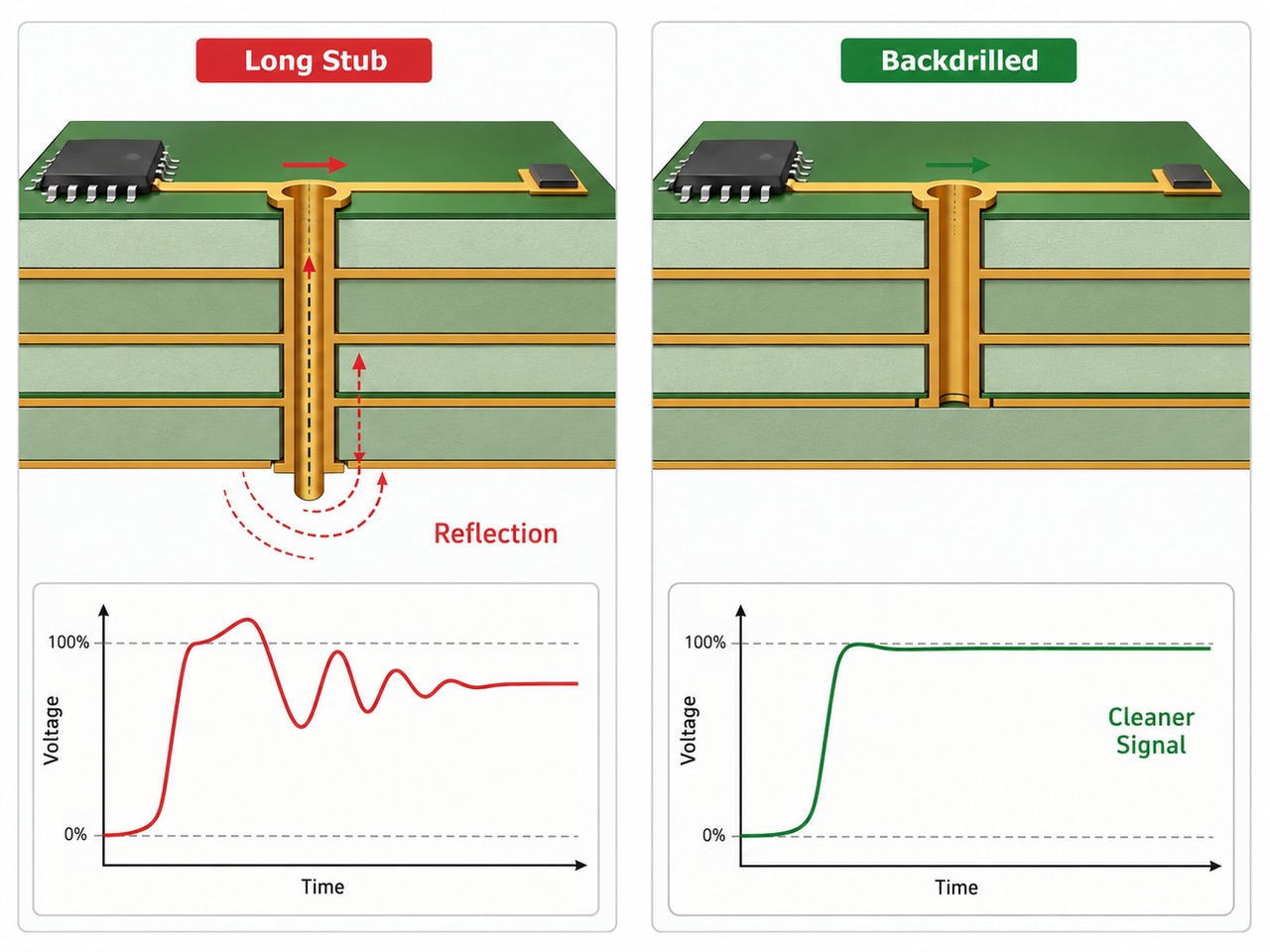
Backdrilling does not remove every via discontinuity. Pads, antipads, the functional barrel, and reference-plane transitions still require careful design.
When Is PCB Backdrilling Required?
PCB backdrilling is justified when the unused barrel creates a measurable channel problem and its removal provides enough performance benefit to cover the added manufacturing work.
Evaluate it when the design has:
- Outer-layer signals connecting to shallow inner layers
- A thick PCB with long vertical interconnects
- High-speed press-fit connectors
- Tight insertion-loss or return-loss limits
- Eye-diagram or simulation failures linked to via resonance
- Blind-via alternatives that would require sequential lamination
It may be unnecessary when the signal uses most of the barrel, the board is thin, the remaining stub is already short, or a routing-layer change solves the issue.
How Does the PCB Backdrill Process Work?
The operation is added after the original through-holes have been drilled and plated.
| Stage | Main operation |
|---|---|
| Engineering review | Confirm stackup, hole locations, drill direction, and stop layers. |
| Primary drilling | Drill the original plated through-holes. |
| Hole plating | Plate copper through the complete barrel. |
| Backdrill setup | Select a larger tool and program each controlled depth. |
| Controlled drilling | Remove the unused plated barrel from the specified side. |
| Inspection | Verify depth, residual stub, and electrical continuity. |
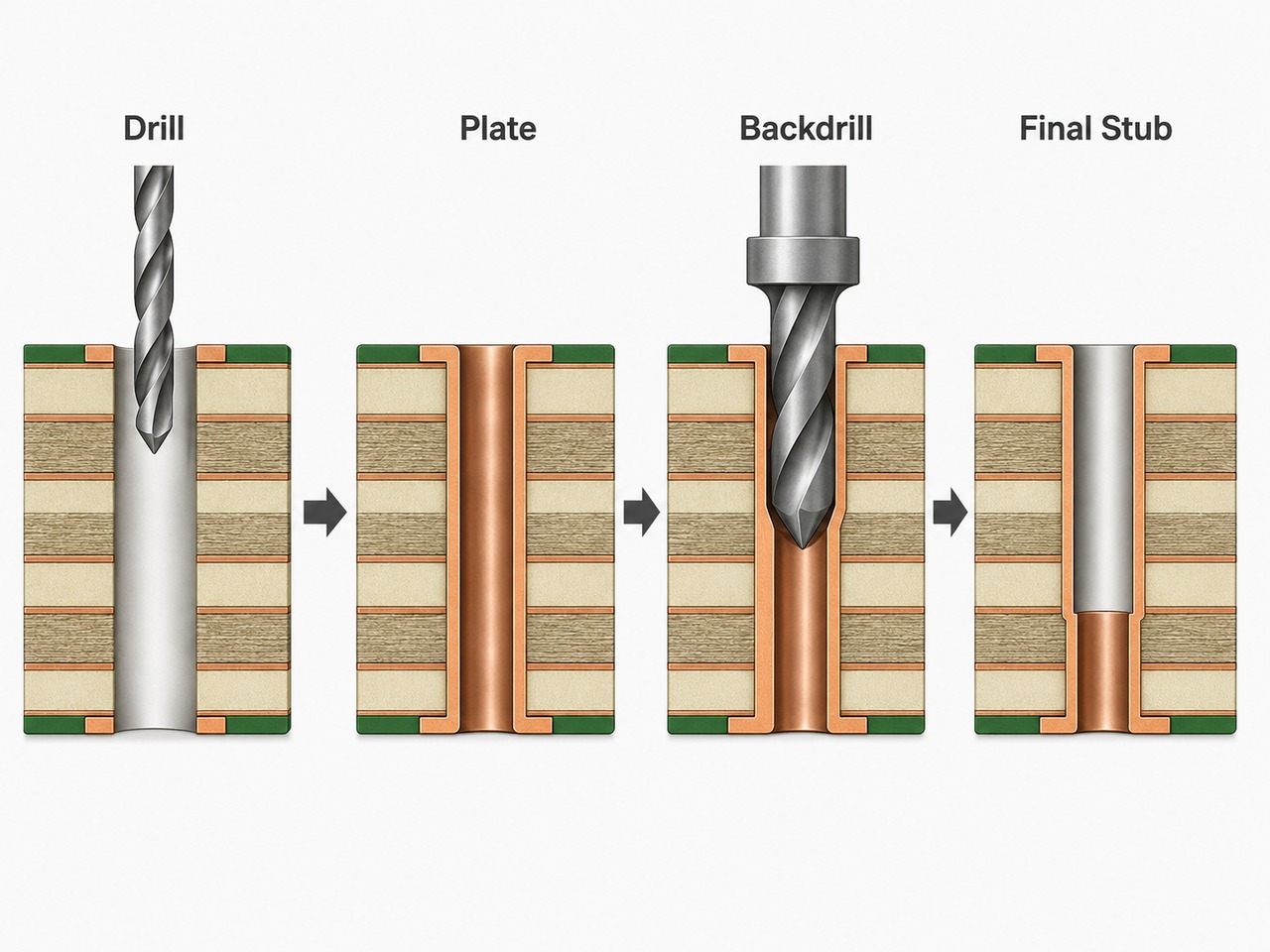
Different connection depths usually require separate programs. The final stackup must therefore be confirmed before the manufacturer calculates drill depth.
What Is an Acceptable Backdrill Stub Length?
The acceptable residual stub must satisfy the electrical target while leaving enough depth margin to protect the final connected layer. Around 10 mils, or 0.25 mm, is a common starting point, although the correct value depends on the channel and the fabricator’s depth-control capability.
The limit is influenced by:
- Signal bandwidth and edge rate
- Laminate dielectric properties
- Board thickness and layer spacing
- Via drill and pad geometry
- Lamination thickness variation
- Backdrill depth tolerance
An unnecessarily short target increases the risk of cutting the connected pad and may add microsection, process-control, and yield costs.
What Are the Main PCB Backdrill Design Rules?
The larger secondary drill needs enough clearance from nearby traces, planes, pads, and adjacent holes.
| Design item | Practical guidance |
|---|---|
| Drill direction | State top, bottom, or both sides. |
| Start and stop layers | Use consistent layer names and numbers. |
| Residual stub | Define the maximum finished stub length. |
| Backdrill diameter | Use a tool larger than the primary drill; a 0.15–0.25 mm increase is a common early-design reference. |
| Copper clearance | Base clearance on the larger backdrill tool and registration tolerance. |
| Non-functional pads | Remove them where they restrict the drilling envelope. |
| Depth groups | Reduce the number of unique depths where routing permits. |
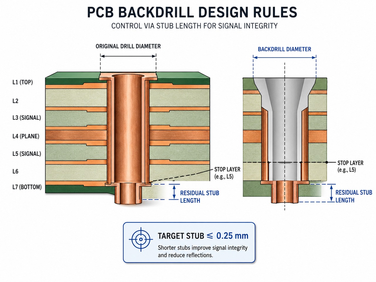
Use these values only for early planning. Final drill sizes, copper clearances, and tolerances must match the selected factory’s process capability.
Can a PCB Be Backdrilled From Both Sides?
Yes. Top-side drilling removes an unused barrel above the active connection, while bottom-side drilling removes the section below it. A via connecting two internal layers may require drilling from both sides.
Double-sided processing can add:
- Separate top and bottom NC files
- More depth groups
- Additional panel handling
- Greater alignment and documentation risk
- More inspection and setup cost
The fabrication drawing must identify the drilling side and stop layer for every hole group.
PCB Backdrill vs Blind Via: What Is the Difference?
Backdrilling is mainly used to improve the electrical performance of a conventional through-hole. Blind vias create partial-depth connections and can also improve routing density.
| Comparison | PCB backdrill | Blind via |
|---|---|---|
| Basic structure | Plated through-hole with part of the barrel removed | Via connects an outer layer to an inner layer |
| Main purpose | Reduce the unused via stub | Create a partial-layer connection |
| Residual stub | A short stub normally remains | No unused through-board barrel |
| Routing density | Similar footprint to a through-hole | Can release routing space on deeper layers |
| Stackup impact | Often uses a conventional multilayer build | May require sequential lamination |
| Cost driver | Hole quantity, depth groups, direction, and inspection | Via structure, plating, and lamination cycles |
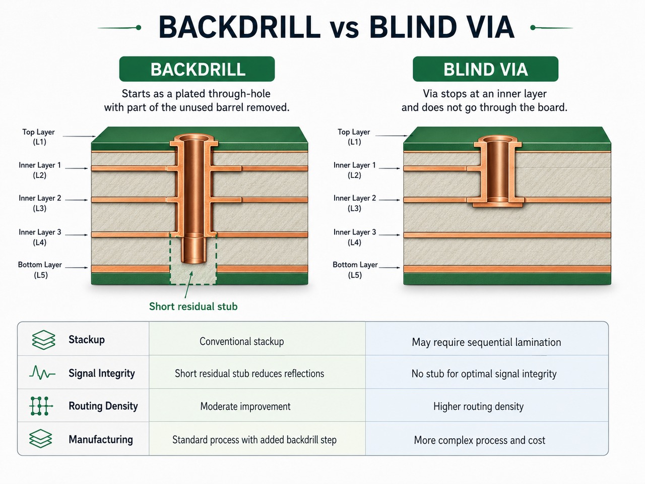
Backdrilling can be more economical when blind vias would add lamination cycles. Blind vias remain attractive when HDI routing density is the main constraint.
What Factors Affect PCB Backdrill Cost?
PCB backdrill cost is based on process complexity rather than a fixed price per hole.
- Hole quantity: More holes increase drill time and tool wear.
- Depth groups: Each unique layer pair may require another setup.
- Drilling direction: Two-sided processing adds handling and alignment work.
- Stub tolerance: Shorter residual stubs require tighter depth control.
- Board construction: Thickness, layer count, hole size, and material affect machinability.
- Inspection: Coupons, microsections, TDR, and reports add cost.
- Order quantity: Prototype setup costs are spread across fewer boards.
Grouping signals around fewer transition depths can reduce both setup cost and CAM complexity.
What Files Are Required for PCB Backdrilling?
A useful quotation package must identify the exact holes, drilling direction, final diameter, layer range, and residual stub limit.
- Gerber, Gerber X2, IPC-2581, or ODB++ data
- Primary plated-hole NC drill file
- Separate backdrill NC files for each depth and side
- Final PCB stackup
- Fabrication drawing and drill table
- Start and stop layers
- Backdrill direction and final tool diameter
- Maximum residual stub
- Controlled-impedance information
- Coupon, microsection, and reporting requirements
Keep layer naming consistent across every file. Mixed layer labels are a common source of CAM interpretation errors.
How Is PCB Backdrill Quality Inspected?
Inspection confirms that the unused copper has been removed without damaging the intended connection.
- Machine calibration: Confirms the programmed depth before panel drilling.
- Backdrill coupon: Reproduces the critical structure outside the functional board.
- Microsection: Measures the actual stub and clearance to the target layer.
- Optical inspection: Checks burrs, debris, and visible misregistration.
- Electrical testing: Detects opens and shorts.
- TDR or impedance testing: Verifies electrical behavior when specified.
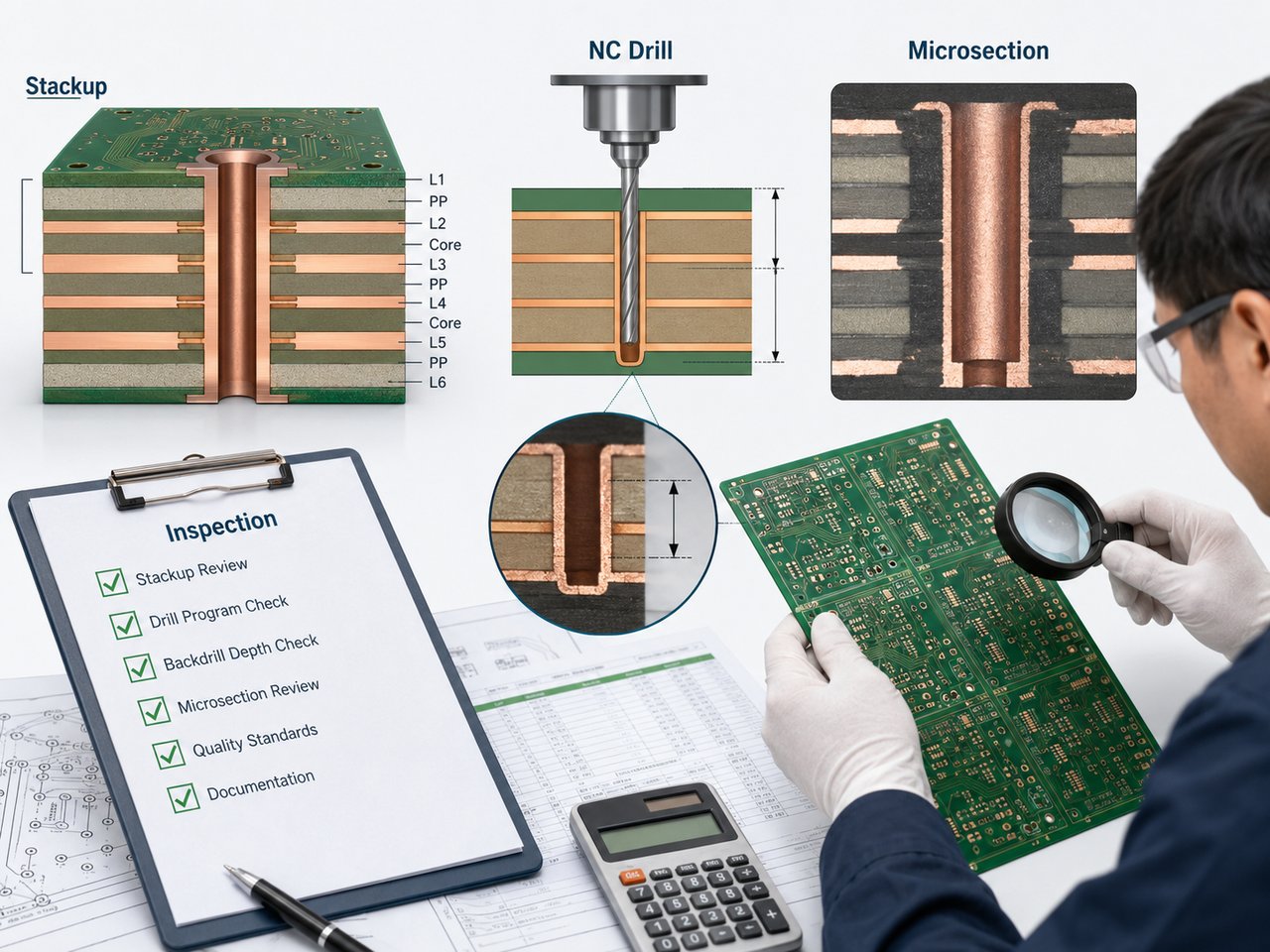
Inspection requirements should be agreed during quotation so that suitable coupons can be included in the production panel.
What Are Common PCB Backdrill Defects?
Most defects come from incorrect data, depth errors, registration errors, or inadequate copper clearance.
| Defect | Possible result | Typical cause |
|---|---|---|
| Excessive residual stub | Remaining reflection or resonance | Drill stopped too early |
| Over-drilling | Open or weakened connection | Drill entered the target layer |
| Remaining barrel copper | Incomplete stub removal | Backdrill tool was too small |
| Exposed nearby copper | Shorting or insulation risk | Insufficient clearance |
| Misregistered backdrill | Partial removal or sidewall damage | X-Y alignment error |
| Wrong drilling side or depth | Stub remains or active barrel is damaged | File-labeling or CAM error |
What Applications Commonly Use PCB Backdrilling?
Backdrilling is most valuable on thick multilayer boards carrying fast signals through long vertical interconnects.
- Data-center servers
- Network switches and routers
- Telecom backplanes and midplanes
- High-speed storage systems
- FPGA and accelerator cards
- PCIe platforms
- Press-fit connector systems
- Test and measurement equipment
- Aerospace communication electronics
- Industrial and medical data-acquisition systems
It usually adds little value to thin, low-speed boards or designs where the signal uses nearly the full through-hole barrel.
How to Prepare a PCB Backdrill Project for Manufacturing
Consider backdrilling before the layout is frozen because the larger tool may require more copper clearance than the original via.
- Confirm the final stackup and finished thickness.
- Identify only the nets that genuinely require backdrilling.
- Define the maximum acceptable residual stub.
- Mark each backdrilled via or connector pin.
- State drilling direction, start layer, and stop layer.
- Specify the final backdrill diameter.
- Check trace, pad, plane, and adjacent-hole clearances.
- Reduce the number of depth groups where routing permits.
- Generate separate NC files for each depth and drilling side.
- State coupon, microsection, and test requirements.
EBest Circuit (Best Technology) can review the layer pairs, drill diameters, copper clearances, and inspection notes before fabrication. Review our PCB manufacturing capabilities and PCB assembly services when defining fabrication, component, inspection, and testing requirements. Early review is most useful while via locations and routing layers can still be changed without a major redesign.
FAQs
Q1. What is PCB backdrill used for?
It removes the unused plated section of a through-hole via to reduce via-stub resonance and reflection.
Q2. What is a via stub in a multilayer PCB?
It is the unused conductive barrel extending beyond the last signal layer connected to the via.
Q3. How short should a PCB backdrill stub be?
Around 10 mils is a common starting target, but the final value must match the channel requirement and drilling-depth tolerance.
Q4. Is backdrilling required for every high-speed PCB?
No. It may be unnecessary when the signal uses most of the barrel or simulation shows adequate channel margin.
Q5. How does backdrilling reduce signal reflection?
It shortens the open-ended via branch that receives and reflects part of the signal energy.
Q6. Is PCB backdrilling cheaper than using blind vias?
It can be cheaper when blind vias would require sequential lamination. Blind vias may still be preferable for HDI routing.
Q7. Can through-hole component holes be backdrilled?
Yes. Press-fit connector holes are a common example when mechanical retention and electrical connectivity remain protected.
Q8. Can a PCB be backdrilled from both sides?
Yes. Two-sided drilling is used when unused barrel sections remain above and below an inner-layer connection.
Q9. Does PCB backdrilling increase lead time?
It can add time for CAM preparation, drill setup, controlled-depth processing, and inspection.
Q10. What files are needed for a PCB backdrill quotation?
Provide the PCB data, final stackup, primary and backdrill drill files, fabrication drawing, drill table, layer pairs, diameter, stub limit, and inspection requirements.
PCB backdrilling is a practical way to reduce via-stub effects without replacing every through-hole with a blind-via structure. It makes the most sense when signal-integrity analysis shows a clear benefit and the design has enough drilling clearance.
For PCB backdrill stackup review, DFM feedback, or quotation support, contact EBest Circuit at sales@bestpcbs.com.







